
2026-08-26 · Conference overview
August 23 to 25, Stanford, Hot Chips 2026. No single chip owned the room; the protagonist was a consensus: the economics of the token is moving the industry's bets from compute density to data movement. This piece first collects the two-day program into one map, then inventories the four directions company by company, and closes with four judgments and testable checkpoints.
The three heaviest signals, the AgentX benchmark and the Vera Rubin measurements, Groq 3 LPU at production scale, and Jalapeño's first scorecard, already have dedicated teardowns; conclusions appear here only where the thread passes through. Every number has been checked against official materials and first-hand reporting, and single-source figures were kept out of the text entirely.
1. The Program Map: Four Directions, Two Through-Lines
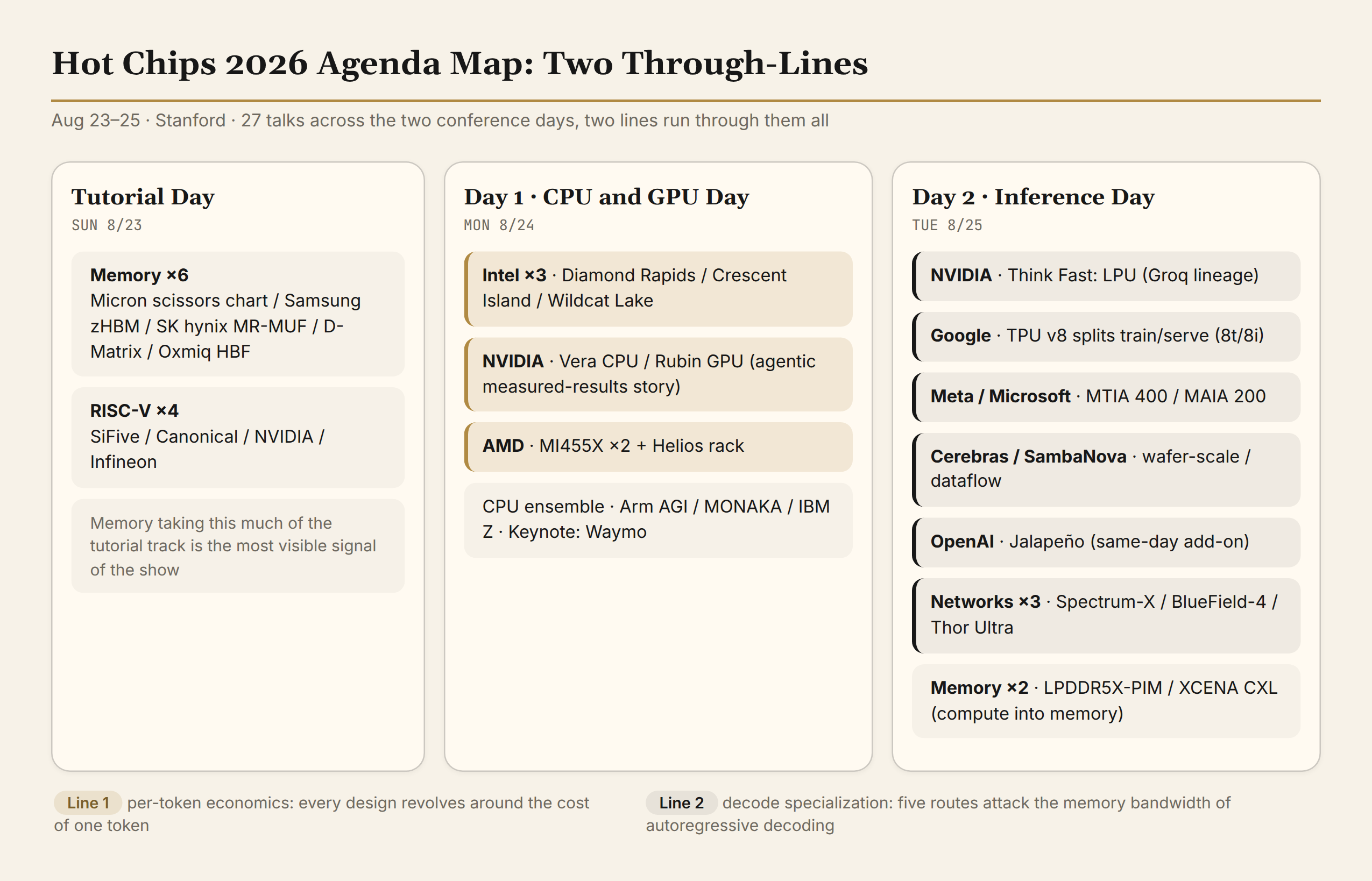
Tutorial day set the tone: six of the ten tutorials were memory, back to back, with Micron, Samsung, and SK hynix all on stage, plus four on RISC-V. Memory taking that much of the tutorial track was the conference's most legible signal: the bottleneck has moved from compute cores to data movement. The two conference days carried 27 official talks. Day 1 ran thirteen: six on CPUs, four on GPUs, with the keynote going to Waymo, the headline topic of a chip conference leaving the datacenter for the road. Day 2 ran fourteen: three on networking, seven AI sessions in a row, with OpenAI's Jalapeño closing the program.
Collected by content, the program falls into four directions: CPUs and the server orchestration layer, who builds the control plane of the inference era; the memory wall, the three makers' ladders plus near-memory compute; AI accelerators, five routes on decode specialization and hyperscaler generation two; and the AI factory network, promoted from connector to factory skeleton. Two through-lines run across both days. Per-token economics: every move by Intel, NVIDIA, and the three memory makers is priced against a single token. Decode specialization: five accelerator routes from very different starting points attacking the same wall, the memory bandwidth of autoregressive decoding. The two lines are causally linked: run the per-token economics to its end, and memory bandwidth in the decode stage becomes the dominant cost item; specialization follows as a corollary.
2. Direction One: The CPU Returns — Who Orchestrates the Inference Era
Six CPU talks put "what does an inference-era server look like" on the table, and every one of them answered the same question: how to cut the cost of a single token.
Intel: A Two-Level Layout, Rack to Edge
Intel had the strongest presence of the week, with three talks in a row; two land in this direction, and the inference flagship Crescent Island sits in the accelerator section.
Diamond Rapids, the orchestration layer. The next-generation Xeon: 18A-P process built in-house, Foveros Direct 3D packaging with UCIe-S interconnect, 256 cores, 1.28GB of LLC, a new APX instruction set with enhanced AMX matrix instructions. Its position: the orchestrator of rack-scale memory and I/O, the foundation under inference clusters.
Wildcat Lake, the edge layer. Core Series 3: low-cost organic packaging, UCIe chiplet interconnect: Intel bringing an open packaging standard into a client SoC for the first time.
The three talks share one through-line: all-homegrown 18A plus open packaging; Intel prices by deployment cost.
NVIDIA: The First Homegrown-Core CPU
Vera, 88 Olympus cores, NVIDIA's first homegrown-core CPU. An ARM v9.2 self-designed core (no longer licensed Neoverse silicon), 176 threads via SMT-X spatial multithreading, 1.2TB/s of SOCAMM2 memory bandwidth, 164MB of L3, single die. It is in full production with the Vera Rubin systems, and with it NVIDIA is entering the server CPU market. Official figures: 1.8× faster agentic task completion and twice the efficiency of traditional x86.
The CPU Ensemble: Usable Threads per Rack Becomes the Selling Point
Arm built a whole-machine chip for the first time: the AGI CPU, TSMC 3nm dual chiplets, 136 Neoverse V3 cores (140 in hardware, 4 held as redundancy), up to 3.5GHz on the 136-core SKU (3.7GHz on the 64-core SKU), aggregate memory throughput over 800GB/s, about 6GB/s per core, putting "usable threads per rack" among the official selling points. Fujitsu's MONAKA leads with the green AI datacenter.
How This Direction Moves
CPUs are no longer the headliners of this conference, but every one of them answers the same question: what the control plane of an inference-era server looks like. The selling points have shifted from clock speed to threads per rack, bandwidth per core, and deployment cost. The orchestration division of labor is taking shape: Diamond Rapids manages rack memory and I/O, Vera manages the heterogeneous system, AGI manages thread density. Two variables to watch: with Arm building a whole-machine chip, the server-CPU market is moving from an x86 duopoly toward an x86–NVIDIA–Arm triangle, and AGI's actual deployments are the first test; and Intel's 18A capacity and yields decide whether "pricing by deployment cost" is a slogan or a price list.
3. Direction Two: The Memory Wall — From a Capacity Race to a Movement Race
Memory was the densest direction on the program: six tutorials back to back, plus two near-memory talks on Day 2. One wall, three ladders, and none of the three makers' answers is simply more HBM.
Micron draws the wall. AI accelerator compute roughly triples every two years; HBM bandwidth grows by less than 2×. That scissors gap is the arithmetic definition of the memory wall, and the starting point of the entire memory agenda.
Samsung stacks upward. A three-step evolution, cHBM to aHBM to zHBM: zHBM abandons the 2.5D interposer and stacks DRAM vertically on top of the XPU; officially, DRAM power down 70%, bandwidth up 2.3×. The name of this ladder is true 3D integration.
SK hynix squeezes inward. MR-MUF packaging extends its lease to 16-high HBM4; copper-to-copper hybrid bonding is explicitly delayed (SK hynix said on stage that it does not meet HBM4e requirements, no earlier than HBM5), and JEDEC's relaxation of the Z-height to 775μm pushed the crossover point further out. The parameters when it finally arrives: 20 layers, core dies 24% thicker, thermal resistance down another 35%, bump pitch pressed from about 30μm to under 18μm.
Compute Moves into Memory: PIM and CXL
Samsung's LPDDR5X-PIM, the first LPDDR-based PIM, is the productization of 2021's Aquabolt-XL, positioned as a lower-cost inference memory route than HBM. The XCENA MX1 is three things in one: CXL 3.0 memory expansion (four DDR5-8400 channels, up to 2TB) plus byte-addressable SSD, plus 3,072 RISC-V cores for near-memory compute.
How This Direction Moves
Three ladders plus PIM and CXL all point to the same shift: the contest has moved from stacking thicker to moving data faster. On the timetable, MR-MUF's lease runs to 16-high HBM4 and hybrid bonding waits for HBM5; zHBM's true 3D integration lands first in specific workloads; and if PIM and CXL deliver on cost, inference memory gains a second market beyond HBM. The variables are JEDEC's Z-height decision and the three makers' 2027 roadmap updates: whoever delivers movement efficiency first takes the next round of spec definition.
4. Direction Three: AI Accelerators — Five Routes on Decode Specialization
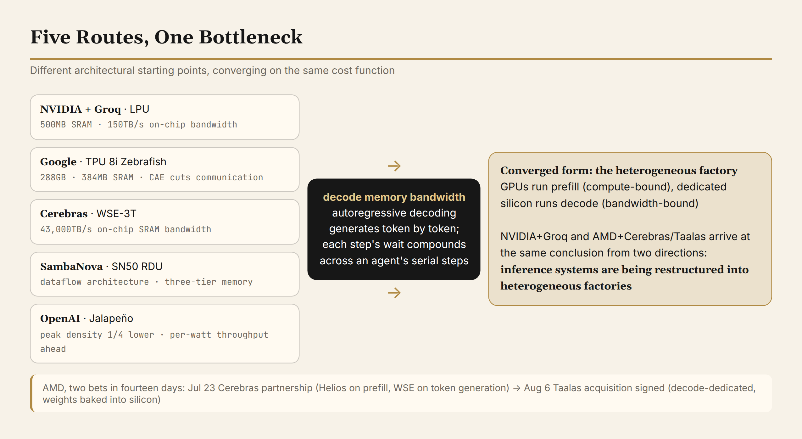
This was the conference's center of gravity: Day 2's seven AI sessions plus Day 1's GPU slots, with the routes converging on one bottleneck: the memory bandwidth of autoregressive decoding. Prefill is bounded by compute; decode, token by token, is bounded by bandwidth, and decode is becoming the dominant cost of interactive inference.
The GPU Camp's Three Answers
NVIDIA: GPUs on prefill, an LPU on decode. Rubin switched the narrative from specs to measurement: the GPU talk is titled Driving the Era of Agentic AI, and the official units of account changed with it: tokens-per-megawatt throughput and cost per token. Vera Rubin NVL72 running DeepSeek-V4-Pro on the AgentX benchmark: up to 30× throughput per MW and up to 35× lower token cost, against GB300 NVL72. Pin the provenance first: these are NVIDIA marketing numbers, and the 30×/35× figures deserve a tiered reading; the independent check, Rubin officially on InferenceX, is still on the calendar. The trend itself is not in dispute: the spec-sheet era is over; see you on the public benchmark is the new rule of the game. On the other side, the third-generation LPU after the Groq acquisition (the Think Fast talk) is in full production, paired with Vera Rubin for heterogeneous inference: 500MB of on-chip SRAM and 150TB/s of on-chip bandwidth per LPU; an LPX rack of 256 units delivering 315 PFLOPS and 640TB/s of aggregate bandwidth; a measured 3,431 tokens/s single-user on Gemma 4 31B, with a DeepSeek-V3-class model needing roughly five racks; an FPGA bridge between the synchronous and asynchronous domains, with speculative decoding swapping only draft tokens; Nebius as the first Token Factory cloud. For the first time, NVIDIA's own reference architecture reserves a formal slot for "not a GPU."
Intel: the inference card that sidesteps HBM. Crescent Island, the first pure-inference GPU on the Xe3P architecture, and the most information-dense chip of the show. 32 Xe3P cores, 256 XMX engines (systolic arrays deepened to sixteen layers), all 3D and ray-tracing hardware deleted, the freed area and power swapped for up to 480GB of LPDDR5X; a 350W air-cooled PCIe card that racks into existing rooms. Every line of the spec compresses deployment cost: sidestep HBM, which is supply-tight and rising in price, with 480GB on paper exceeding Rubin's 288GB and MI455X's 432GB; air cooling skips the liquid-loop retrofit. The stated design goal is blunt: tokens per watt and agentic workloads, with native vLLM, SGLang, and llm-d support. Sampling in H2 2026, on the market in 2027.
AMD: the rack, plus two bets. Two MI455X talks assembled the complete 72-GPU rack: 12 HBM4 stacks totaling 432GB at 23.3TB/s, UALink open interconnect, and the EPYC Venice CPU plus Pensando Vulcano AI NIC as a co-designed trio; the first rack was installed in Texas in June, with Meta deploying this year. Then, within fourteen days, two transactions: July 23, the Cerebras partnership, Helios on prefill and the WSE on token generation; August 6, the agreement to acquire Taalas (closing in Q4), whose decode-dedicated chips hard-wire model weights into silicon. Instinct takes prefill, Taalas takes decode, both exposed uniformly through ROCm. One distinction is worth drawing here: The Register's verdict in its Jalapeño coverage, that Taalas bets performance on one specific model while sacrificing programmability, holds at the general-purpose-accelerator layer; as the decode-dedicated die inside the rack, it is now on the Helios roadmap, and the two identities do not conflict.
Hyperscaler Silicon: The Training/Inference Split and the Flagships
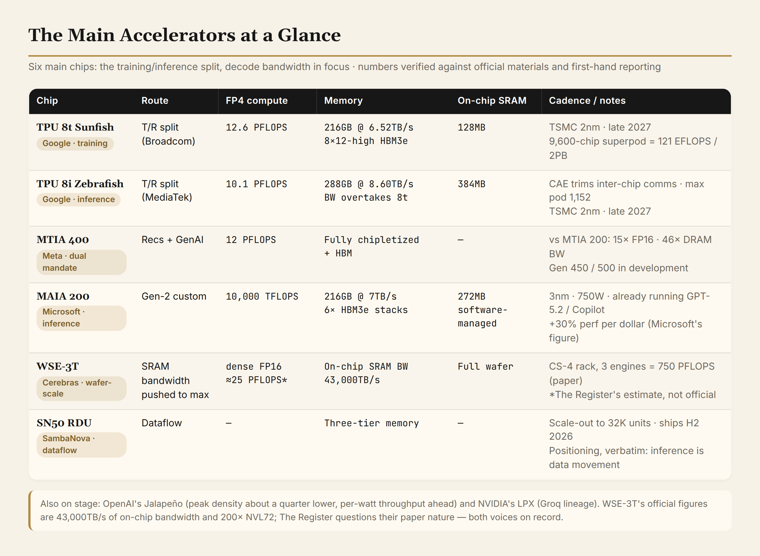
Google, the eighth TPU splits training and inference for the first time, and the evidence is written into the spec sheet. The 8t Sunfish (training, designed with Broadcom): 12.6 PFLOPS FP4, 216GB of HBM, 6.52TB/s, 128MB of on-chip SRAM; a 9,600-chip superpod at 121 exaflops over 2PB of shared memory, doubled ICI bandwidth, and scale-out to 134,000 chips on the Virgo fabric. The 8i Zebrafish (inference, designed with MediaTek): 10.1 PFLOPS FP4, 288GB of HBM, 8.60TB/s, 384MB of on-chip SRAM (bandwidth and SRAM overtaking the 8t, compute slightly lower, maximum pod 1,152 chips); a new Collectives Acceleration Engine trims inter-chip communication, and the Boardfly topology replaces the 3D torus, designed for the latency targets of MoE serving. Training stacks pod scale; inference stacks bandwidth and SRAM. Each chip is optimized to its own objective: the training/inference split has reached silicon itself.
Meta MTIA 400, from a recommendation-only mandate to recommendation plus GenAI. 12 PFLOPS FP4; against MTIA 200: 15× the FP16 compute, 46× the DRAM bandwidth, 5× the SRAM bandwidth; fully chipletized with two compute dies, one SoC, and two network dies plus HBM, an 8×6 PE array with a redundancy row; the next generation, 450 and 500, already in development.
Microsoft MAIA 200, from a chip to a datacenter-scale system. TSMC 3nm, 140 billion transistors, an 820mm² SoC die with 10,000 TFLOPS of FP4 compute; six HBM3e stacks totaling 216GB at 7TB/s; 272MB of on-chip SRAM managed explicitly by software; fully connected quad topology with unified Ethernet scale-up; 750W. Already carrying GPT-5.2, Microsoft 365 Copilot, and Foundry; Microsoft's figure of 30% better performance per dollar than the current fleet is self-reported, with the 2027 financial-report TCO still to come. Custom silicon has moved from cost-side experimentation to carrying flagship loads: a structural change of position.
Two Extreme Samples of the Bandwidth Logic
Cerebras amplifies at wafer scale. The CS-4 rack integrates three WSE-3T engines into Nexus: 44GB of on-chip SRAM and 43,000TB/s of on-chip bandwidth per engine; the rack totaling 750 PFLOPS and 129.6PB/s of aggregate memory bandwidth (officially rated), with 53.5PB/s of fabric bandwidth, over 200× the scale-up bandwidth of NVL72 per the company; shipping this quarter. The Register offers a different set of estimates: the WSE-3T is the same silicon as the WSE-3 run harder, dense FP16 works out to roughly 25 PFLOPS, and how much of the aggregate bandwidth figure is real remains open. Its value is as the control group: the physical-limit sample of the "push memory bandwidth to the extreme" logic.
SambaNova takes the dataflow route. The fifth-generation SN50 RDU, built for agentic inference, three-tier memory architecture, scale-out to 32K units, shipping in H2 2026. The company's positioning, verbatim: inference is a data movement and memory optimization problem, and it calls for a different architectural approach.
Add OpenAI's Jalapeño, which closed the program, and the picture is five routes, NVIDIA, Google, Cerebras, SambaNova, and OpenAI, with AMD following within fourteen days with two transactions of its own: decode specialization has gone from one company's wager to an industry-scale migration.
The key specs of the main accelerators, one table:
How This Direction Moves
The five routes solve the same cost function; they differ only in starting point: the GPU camp splits heterogeneous duties inside existing architectures, the hyperscalers customize silicon to their own workloads (the TPU split outright), and the extreme samples push the bandwidth logic to physical limits. The division of labor is sinking from the scheduler into the mask set: the TPU split into 8t and 8i, the LPU stands beside the GPU in the reference architecture, AMD bought a decode-dedicated chip company outright. The biggest variable ahead is measured truth: every vendor's numbers are self-reported; until independent benchmarks arrive, they should all be heard at a discount. One level down: whether Intel's tokens-per-watt holds up against same-generation rivals, and when hyperscaler generation two delivers verifiable TCO.
5. Direction Four: The Network Becomes the AI Factory Skeleton
Broadcom's Thor Ultra led off: an 800GbE AI/HPC NIC. NVIDIA's Spectrum-X multi-plane splits the AI factory into five purpose-built networks: scale-across, scale-out, scale-up, and AI context, plus the newly announced scale-in, on the claim that no single general-purpose fabric can serve all five traffic classes; addressable scale expands from 8K to 512K GPUs, a factor of 64, with co-packaged optics in production. BlueField-4 is co-designed into every Vera Rubin, Astra aggregating 7Tb/s, positioned as the AI factory operating system.
How This Direction Moves
Decode specialization exposes the factory-scale question: the more heterogeneous the chips, the more valuable the fabric that weaves them, and the network is being promoted from connector to factory skeleton. Running parallel is a second front, open interconnect: UCIe, UALink, unified Ethernet, NVLink Fusion; outside NVIDIA's own ecosystem, nearly every player is standardizing the interconnect. Two variables: whether the "no single general-purpose fabric suffices" claim meets a counterexample, and how fast co-packaged optics' production cost curve falls.
6. The Two Through-Lines Are One Story: Four Judgments
Stack the four directions and the causal chain closes. The denominator of per-token cost is power and data movement: compute density keeps rising, but Micron's scissors say more and more of the added FLOPS spend their time waiting for data; the bandwidth bottleneck of token-by-token decode is further amplified by agents' serial steps, every wait compounding. General-purpose GPUs do have one standard answer left, bigger batches amortizing bandwidth cost across more requests, but that road has topped out under interactive-latency constraints, and the matched-TBT measurements from Jalapeño are the footnote. One solution remains: split decode out of general-purpose compute and hand it to specialized silicon. The five routes are five solutions of the same cost function.
The minimal sample is already in hand: Jalapeño's B0 and Rubin's die, same process and similar size, peak density about a quarter lower, per-watt throughput ahead, the gap traced to data movement and phase-aware scheduling. The two-day program is that sample at scale. On this causal chain, four industry judgments:
Judgment one: the training/inference division of labor has sunk to silicon. The system-level prefill/decode separation became silicon at this show: the TPU split into 8t and 8i, the LPU standing alongside the GPU in NVIDIA's reference architecture, AMD buying a decode-dedicated chip company and signing a wafer-scale partner within two weeks. The prefill/decode boundary used to be drawn by the scheduler; it is now written directly into the mask set.
Judgment two: open interconnect is the second united front. UCIe entered an Intel client SoC; UALink underpins Helios's 72 GPUs; MAIA 200 uses unified Ethernet for scale-up; NVLink Fusion is opening its door to the RISC-V ecosystem. Outside NVIDIA's own ecosystem, nearly every player is standardizing the interconnect; CPO production presses optics further into the switch. The first front is decode specialization; this is its mirror image: the more heterogeneous the chips, the more open the interconnect must be.
Judgment three: the memory-wall battlefield shifts from capacity to movement. None of the three makers' answers is simply more HBM: zHBM cuts interconnect-layer power; MR-MUF and hybrid bonding compress thermal resistance and pitch inside the package; PIM and CXL move compute to the data outright. The capacity race is over; the movement race has begun.
Judgment four: benchmark framing is the new battleground. NVIDIA now tells its story in tokens per MW, Intel writes tokens per watt into product goals, Microsoft self-reports 30% better performance per dollar: every vendor picking the yardstick that flatters it. On self-reported numbers of this kind we apply a uniform 30-percent discount; until independent benchmarks land, the discount stays. The independent check of Rubin on InferenceX is the first touchstone of the entire consensus.
So the consensus of this Hot Chips can be written in one line: the era of stacking FLOPS for training is over; the inference era runs on memory bandwidth, data movement, and heterogeneous division of labor. NVIDIA plus Groq and AMD plus Cerebras converge on the same conclusion from two directions: the inference system is decomposing into a heterogeneous factory.
7. Predictions and What to Watch Next
Put the four directions side by side and the whole show comes into view at once: 27 official talks; Intel's triple launch centered on deployment cost; NVIDIA's first homegrown-core CPU; AMD's open rack; Arm's first whole-machine chip; five routes on decode attacking one bottleneck; the hyperscaler camp moving up a generation; the memory trio moving from capacity to movement; the network re-arranged into five fabrics. The four judgments, restated as testable predictions, with checkpoints we will return to verify:
- The empirical base of decode specialization. Prediction: independent measurements will support the magnitude judgment that decode bandwidth dominates cost. Checkpoints: Rubin's independent run on InferenceX, and LPX measurements once Nebius's Token Factory goes live. If independent numbers land materially below self-reported ones, or heterogeneous LPX deployment slips, the industry-migration judgment needs re-weighing.
- Intel's tokens-per-watt awaits measured proof. Prediction: Crescent Island's tokens-per-watt will be competitive against same-generation rivals. Checkpoints: third-party measurements after H2 2026 sampling, and 2027 launch pricing.
- The mettle of hyperscaler generation two. Prediction: MAIA 200's per-dollar advantage will narrow under financial-report accounting, but the direction holds. Checkpoint: TCO data in Microsoft's 2027 reports.
- The memory-wall timetable. Prediction: hybrid bonding slips to HBM5 per SK hynix's line, and zHBM lands first in specific workloads. Checkpoints: the three makers' 2027 roadmap updates, and JEDEC's Z-height decision.
Data as of 2026-08-29. Specs and mechanisms from Hot Chips 2026 vendor presentation materials, official releases, and on-site reporting (ServeTheHome among others); self-reported figures and single-source restatements are flagged in the text.
Further reading: Dissecting SemiAnalysis AgentX · From a Lone Bet to Consensus: Groq 3 LPX Reaches Production · OpenAI Turns In Its Scorecard: Jalapeño's First Measured Results · The SubQ Three-Month Audit (the earlier memory-wall piece)