Inside Jalapeño: What Happens When an AI Company Builds Its Own Heart
On June 24, 2026, OpenAI and Broadcom jointly released Jalapeño, OpenAI's first in-house AI inference chip. From architecture to tape-out in just 9 months, with inference costs projected to drop ~50% and performance matching NVIDIA Blackwell and Google TPU. First deployment by end of 2026, scaling to 10GW of compute capacity by 2029. This is not just a chip. It is the moment OpenAI pivots from "AI company" to "AI full-stack company", and the moment the AI industry's supply chain logic starts to be rewritten.
Introduction: Three and a Half Years from ChatGPT to Jalapeño
Rewind to November 30, 2022—the day ChatGPT launched. Back then, OpenAI was still a "model company." Its compute lived in NVIDIA GPU clusters inside Microsoft Azure, and the trained models were exposed to the world through the OpenAI API. Nobody imagined that the same company would, three and a half years later, stand in a Broadcom office in Silicon Valley and receive a wafer it designed itself from Hock Tan's hands.
But the story of Jalapeño isn't "an AI company suddenly gained chip-making ability." It's the final landing of a series of decisions:
- End of 2023: Richard Ho (a core engineer from Google's Cloud TPU team) joined OpenAI and began building a chip team
- Mid-2024: OpenAI and Broadcom started secret joint development (the "pre-phase" of the 18-month cycle)
- October 2025: The partnership was publicly disclosed—tens of billions of dollars, 10GW deployment target
- June 24, 2026: Jalapeño officially released; engineering samples already running GPT-5.3-Codex-Spark
The chip's name, Jalapeño (Mexican pepper), continues Google's TPU tradition of naming chips after snacks (Boardwalk, Bristlecone, Trillium), with OpenAI's signature "seemingly casual, actually precise" branding. The naming style makes it impossible to take as seriously as "B100" or "MI300X," but its strategic significance far exceeds what the name conveys.
This article will dissect Jalapeño's:
- Designers . Google TPU soul + 40-person minimalist team + Broadcom's ASIC engineering power
- Manufacturing . TSMC 3nm + Broadcom silicon implementation + Celestica system integration
- Positioning . Why "inference-only, not training" is the only commercially correct choice
- Architecture and Specifications . Systolic array, HBM, Arm CPU, Tomahawk interconnect
- Process & Compute. vs Google TPU v7/v8 and Blackwell compute, efficiency, HBM
- Physical Analysis. 3nm, Die Size, transistor count, packaging, thermal, memory
- Software Adaptation. Vertical integration advantages and ecosystem lock-in costs
- Horizontal Comparison. vs NVIDIA / Google TPU / AWS / Microsoft
- China Vendor Panorama. Alibaba, ByteDance, DeepSeek, Zhipu
- Conclusion. The next form of an AI company
1. Designers: The Soul Out of Google TPU
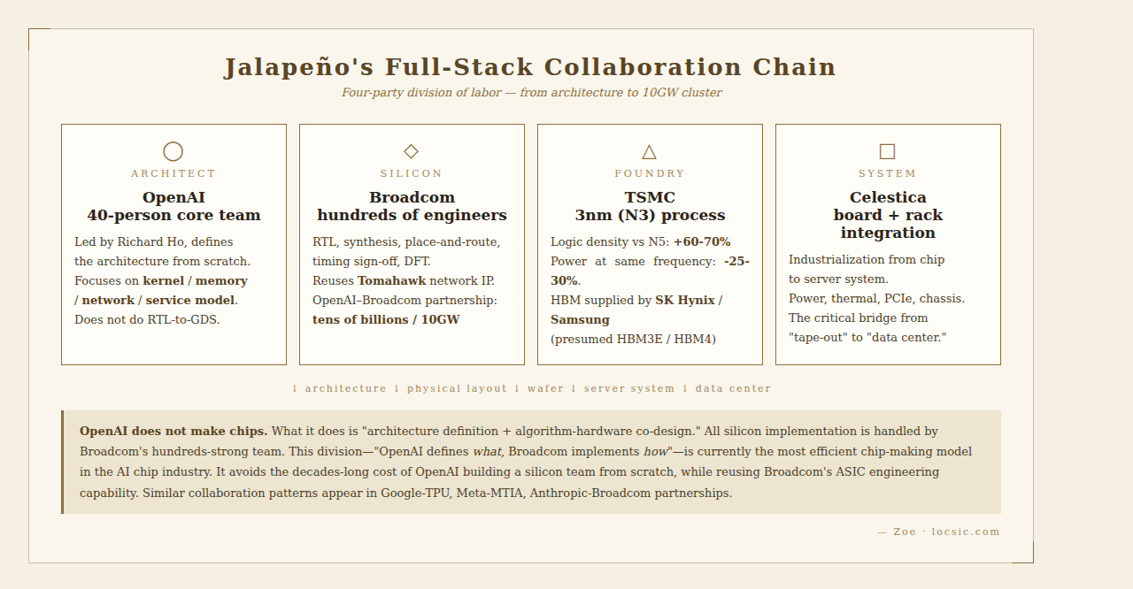
The Core Engineer: Richard Ho
The soul of Jalapeño is OpenAI's hardware project lead, Richard Ho. He previously spent nearly nine years at Google, where he was a core architect on the Cloud TPU project, leading multiple TPU generations from concept to mass production.
Richard Ho's key background:
- 2014–2023: Google TPU team, designer of systolic array architecture, memory hierarchy, on-chip network, and other critical modules
- Witnessed the full evolution from TPU v1 (2016) to TPU v7 Ironwood (2025)
- Has the most direct engineering understanding of why the ASIC route works, why Tomahawk-class interconnect is necessary, why HBM selection is so critical
End of 2023, Sam Altman began aggressively recruiting from Google's TPU team. Richard Ho joined OpenAI during this period and led the formation of the Jalapeño team.
The signal from this personnel flow is extremely clear: OpenAI knew the ASIC route was viable, but needed people who had already learned all the lessons from TPU.not explorers starting from scratch. Richard Ho knows which pitfalls to avoid.
The OpenAI Chip Team: 40 People, Minimalist Architecture
At the time of release, OpenAI's chip team numbered approximately 40 people. To put this in context:
| Team | Size | Notes |
|---|---|---|
| OpenAI Jalapeño team | ~40 people | Architecture design |
| Google TPU team | Thousands | Includes compiler, software, verification |
| NVIDIA GPU design team | Tens of thousands | Spans multiple product lines |
| Apple Silicon team | Thousands | Includes SoC, GPU, Neural Engine |
Why can 40 people build a chip?
Because OpenAI's 40 people do only one thing—architecture definition and algorithm-hardware co-design. All RTL-to-GDS (from synthesizable code to physical layout) silicon implementation is handled by Broadcom's hundreds-strong team. This "OpenAI defines 'what to do', Broadcom implements 'how to do it'" division of labor is the most efficient chip-making model in the current AI chip industry.
Broadcom: The Real Silicon Implementation Power
Broadcom is the true giant of ASIC design services:
- Existing clients: Google, Amazon, Meta, ByteDance, Anthropic
- AI ASIC design capability: From Tomahawk networking chips to TPU physical implementation.all Broadcom
- October 2025: Strategic partnership signed with OpenAI, 10GW deployment target
- CEO Hock Tan personally oversaw: At the launch event, he personally handed the first wafers to Sam Altman
Broadcom's role is not just "foundry" but an extension of OpenAI's chip team. Everything from RTL, verification, synthesis, place-and-route, timing sign-off, to Tomahawk network chip integration is handled by Broadcom.
Celestica
The Canadian electronics manufacturing services provider handles board, rack, and server system industrialization. Celestica's role is underestimated—going from a chip to a deployable server requires power management, thermal design, PCIe interfaces, chassis structure, and a lot more engineering. Celestica is the critical bridge from "successful tape-out" to "data center ready" for OpenAI.
2. Manufacturing: TSMC 3nm + Broadcom Silicon Implementation
Jalapeño's manufacturing division is a typical AI-era ASIC collaboration network:
| Link | Owner | Notes |
|---|---|---|
| Architecture design | OpenAI | Blank-slate design, built from zero around LLM inference |
| Silicon implementation (RTL-to-GDS) | Broadcom | Physical design, timing sign-off, DFT |
| Wafer foundry | TSMC | 3nm (N3) advanced process |
| Network interconnect | Broadcom | Tomahawk networking chips (rack/cluster interconnect) |
| Board/rack | Celestica | Industrialization from chip to server system |
| HBM supply | SK Hynix / Samsung | High-bandwidth memory (presumed HBM3E or HBM4) |
What TSMC 3nm Really Means
The industry needs to be honest about what "3nm" means. TSMC N3's actual physical gate length no longer shrinks; "3nm" is mostly a marketing name. But there are some objectively comparable numbers:
- TSMC N3 vs N5: logic density +60-70%, same-frequency power -25-30%
- N3 capacity at TSMC is extremely tight.Apple, AMD, NVIDIA, MediaTek, and Broadcom clients are all fighting for it
- TSMC has notified 5-10% price increases for 3-5nm customers
For OpenAI, getting a tape-out slot on N3 is itself a hidden resource brought by Broadcom's long-term customer relationships.
9 Months to Tape-Out: "The Fastest ASIC Development Cycle in History" (OpenAI's Claim)
Jalapeño took only 9 months from architecture design to tape-out. OpenAI claims this is "the fastest ASIC development cycle in the history of high-performance advanced semiconductors." Comparisons:
| Comparable | Development Cycle |
|---|---|
| OpenAI Jalapeño | 9 months (architecture to tape-out) |
| Google TPU v1 | ~15 months (start to deployment) |
| Google TPU v2-v4 | 12-18 months/generation |
| AWS Trainium v1 → v2 | ~24 months |
| Apple M-series | 24-36 months |
| Traditional chip company comparable projects | 24-36 months |
⚠️ Analysts on Zhihu point out that "9 months" may be counted from some intermediate node. OpenAI and Broadcom's joint development actually started in mid-2024 (described by media at the time as "18 months of secret R&D"), and actual architecture exploration may have begun earlier. Compressing "18 months" into "9 months" is a PR choice, but even so, it's extremely fast.
The Real Substance Behind "9 Months"
Breaking down the time savings:
| Time-saving Source | Estimated Contribution |
|---|---|
| 18 months of pre-architecture exploration and Broadcom collaboration groundwork | 3-4 months saved (counted into "formal R&D") |
| AI-accelerated PPA optimization (DSO.ai / Cerebrus-class tools) | 2-3 months saved |
| Broadcom IP reuse (Tomahawk, SerDes, HBM PHY) | 2-3 months saved |
| AI-accelerated verification, thermal simulation, sign-off | 1-2 months saved |
| Traditional circuit design and tape-out prep | 2-3 months (still required) |
OpenAI didn't perform a miracle.they used every available tool in the industry to the extreme, plus Broadcom's ASIC engineering reuse, to compress the timeline to 9 months.
3. Positioning: Inference ASIC, Not Training Chip
"Intelligence Processor"—OpenAI's Name for Its Own Chip
This is not marketing language; it defines the essential difference from a GPU.
Jalapeño does not do training, only inference.
| Dimension | Training | Inference |
|---|---|---|
| Purpose | Make the model learn | Make the model answer questions |
| Characteristics | One-time, high precision, crazy compute | Continuous operation, latency-sensitive, cost-king |
| Cost nature | Capital expenditure (CAPEX) | Operating expenditure (OPEX) |
| OpenAI 2025 H1 inference spend | . | $5.02 billion |
| Industry estimate of inference share | . | Inference ~60-70% of total AI operating cost (industry-standard estimate) |
Why 2026 Is the Right Time
Launching an inference chip in 2023 would have been too risky.the model architecture was iterating rapidly (from pure Transformer to MoE to hybrid architectures), and an ASIC could be obsolete by the time it shipped. By 2026, Transformer + MoE has become the dominant paradigm, architecture has stabilized, and the commercial risk of custom ASICs has dropped to an acceptable range.
Three strategic considerations:
- Technology maturity window: Model architecture is stable; the ASIC won't fall behind
- Commercial pressure tipping point: Inference costs crossed a critical threshold in 2025; a cost-reduction solution is needed
- Supply chain diversification "floor": Break free from single dependence on NVIDIA
Business Logic: Breaking NVIDIA Dependence
OpenAI compute infrastructure history:
- 2023–2024: ~20,000 H100 (GPT-4 training + inference)
- 2025: H200 + Grace Hopper (GPT-5 training)
- 2026: B200/GB200 (multimodal model training)
Cost structure: In 2025, OpenAI's total spending was $34 billion, revenue $13 billion, net loss $20.9 billion. H1 inference spend was $5.02 billion (annualized ~$10B), accounting for ~30% of total spending (OpenAI's own figures). The industry-standard estimate is that inference is 60-70% of total AI operating cost.the gap between the two calibers is whether "AI operating cost" includes training or not. CFO Sarah Friar has warned: if revenue growth doesn't keep up with data center contract expansion, compute costs could soar to $85 billion by 2028.
Jalapeño targets directly the most frequent and most expensive segment.inference. If Hock Tan's "50% cost reduction" claim holds, it means:
- Per-token cost halved → ChatGPT free user service capacity doubles
- Same budget serves more users → directly affects OpenAI's break-even point
- Same conditions free up budget for training (still buying NVIDIA GPUs) → overall compute expansion accelerates
4. Architecture and Specifications: Systolic Array, HBM, Arm CPU, Tomahawk Interconnect
Core Architecture: Systolic Array
The Systolic Array is the AI accelerator architecture pioneered by Google's TPU v1 (2016). The name comes from cardiac systole—data flows regularly between processing elements (PEs) like blood, with each PE repeatedly doing the same thing (typically multiply-accumulate).
OpenAI's choice of systolic array is doubling down on a paradigm already validated by Google, not adventurously experimenting.
Benefits of Systolic Array for Dense Model Inference
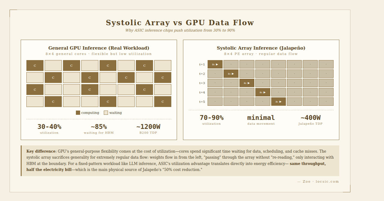
Dense models (like Llama-3-70B style) have all parameters participating in computation during every inference.
- Data Movement Minimization
- Traditional GPU: each CUDA core requires independent register read/write
- Systolic array: weights flow in from the left, "passing" through the array without "re-reading," only interacting with HBM at the boundary
- Less data movement = direct power savings = improved performance per watt
- Extreme Compute Density
- A 128×128 systolic array = 16,384 MAC units, all working simultaneously
- Doesn't need very high frequency, but completes ~3.3 trillion INT8 ops/sec
- Perfect for the Transformer "matrix multiply → matrix multiply → matrix multiply" pattern
- Regular Data Flow
- Batch size and sequence length are relatively stable during inference
- Doesn't need the GPU's flexibility to "run any computation pattern"
- Hardware utilization can stay stable at 70-90% (far above GPU's 30-40%)
Systolic Array for MoE: Matches and Conflicts
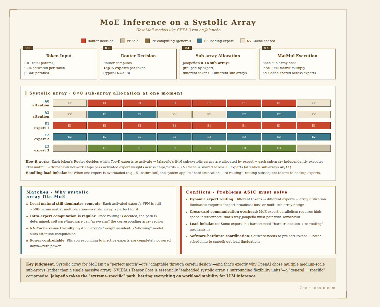
OpenAI's GPT-4 / GPT-5 / GPT-5.3 are all based on the MoE architecture. MoE has two key features:
- Sparse activation: 1.8 trillion total parameters, but only 2% (~36 billion) activated per token
- Expert routing: Router dynamically selects Top-K experts for each token (typical K=2~8)
Matches
- Local Matrix Multiplication Still Dominates Compute
- Even with MoE, the FFN computation inside activated experts is still huge matrix multiplication
- DeepSeek-R1's activated expert FFN: ~50B params × batch × seq_len
- This part is fully suited to systolic array's high-density matrix multiplication
- Intra-Expert Computation Is Regular
- Once the Router decides which experts to activate, the subsequent matrix multiply path is determined
- Software/hardware can "pre-warm" the corresponding systolic array regions in advance
- This predictability + local regularity is the sweet spot for systolic arrays
- KV Cache Reuse Friendly
- In MoE inference, the attention layer's KV Cache is shared across all experts
- The systolic array data flow model is well-suited to "weight resident, KV data flow" attention computation
Conflicts
- Dynamic Expert Routing
- Different tokens go to different experts → array utilization may fluctuate wildly
- If K=2, perhaps only 25% of the array is busy
- Response: Hardware reserves "expert broadcast bus" so array sections can load different expert weights; or token sorting for batch scheduling
- Increased Communication Overhead
- MoE's "Expert Parallelism" inherently requires cross-card communication
- After routing, the activated experts may be on different chips
- This is why OpenAI must use Broadcom Tomahawk (high-speed interconnect) for large-scale clusters
- Load Imbalance
- Router probability distribution may cause certain experts to be selected more often
- Requires "hard truncation + re-routing" mechanisms
- Systolic arrays are sensitive to this imbalance because the PE array is physically fixed
Inferred Jalapeño Response Strategy
Although no ISA documentation is public, from OpenAI's emphasis on "designed from zero for LLM inference" we can infer:
- Array scale may not be a single oversized array, but multiple medium-scale systolic arrays (e.g., 8-16 sub-arrays of 64×64)
- Can flexibly assign experts to different sub-arrays based on routing results
- Tomahawk network chips support large-scale expert parallelism, extending "hardware sparsity" to "cluster sparsity"
Confirmed Technical Details
| Item | Estimated/Confirmed |
|---|---|
| Process | TSMC N3 |
| Core architecture | Systolic Array |
| Memory | HBM3E or HBM4 (estimated 80-144GB) |
| Task scheduling CPU | Arm custom design |
| Network interconnect | Broadcom Tomahawk series switches |
| Theoretical compute (est.) | ~10-13 PFLOPS (INT8/FP8) |
| Per-token energy | ~30% lower than Blackwell |
| Inference cost reduction | ~50% (Hock Tan) |
Four Optimization Dimensions (Richard Ho)
OpenAI's hardware lead emphasized Jalapeño has comprehensive optimization across four dimensions:
- Kernel . Hardware-level hardcoding for LLM core operators (matrix multiply, attention)
- Memory Movement . Reducing data shuttling between HBM and compute units
- Network . Tomahawk enables low-latency interconnect for large-scale clusters
- Service Model . Co-optimization for online inference batching, KV Cache residency, etc.
These four optimizations let the chip's real-world utilization approach theoretical peak, unlike GPUs that have "high peak, low utilization (30-40%)."
5. Process and Compute Estimation: vs Google TPU v7/v8
Process Estimation Basics
TSMC N3 vs N5: logic density +60-70%, same-frequency power -25-30%. This is an objective benchmark, applicable to all N3 customers.
Google TPU Known Key Data
| Chip | Release | Process | FP8 Compute/Chip | HBM | Cluster Scale | Notes |
|---|---|---|---|---|---|---|
| TPU v6 Trillium | 2024.5 | 5nm | ~1 PFLOPS | 32GB | 256 cards | 4.7x v5e performance |
| TPU v7 Ironwood | 2025.11 | TSMC 3nm | 4.6 PFLOPS | 192GB HBM3E | 9,216 cards (42.5 EFLOPS) | 100% liquid cooling, ~980W |
| TPU 8t "Sunfish" | Released 2026.4 | Est. 3nm | Est. ~12 PFLOPS | Est. 192GB+ | Same | Training-only, Broadcom design |
| TPU 8i "Zebrafish" | Released 2026.4 | Est. 3nm | Est. 3-4 PFLOPS | 384MB SRAM×3 | Same | Inference-only, MediaTek design |
Jalapeño Compute Estimation
OpenAI didn't disclose die size, HBM count, or transistor count. But there are public clues:
- Process: TSMC N3 (same generation as TPU v7 Ironwood)
- Network: Broadcom Tomahawk
- Hock Tan claims "performance comparable to Blackwell"
Using TPU v7 Ironwood's 4.6 PFLOPS as baseline.NVIDIA Blackwell B200 in FP8 is 20 PFLOPS, but that's a dual-die, 208 billion transistors, 1600mm² die size, 1200W TDP monster.
Jalapeño's compute estimate must be done in two steps.
(a) FP8 peak compute estimate (direct Blackwell comparison):
- Reason 1: ASIC architecture is more efficient than GPU; same transistor budget yields more equivalent compute
- Reason 2: Hock Tan says "comparable to Blackwell".this refers to effective throughput (see b), not direct FP8 peak comparison
- Reason 3: Lei Tech's "10 PFLOPS" speculation falls in a reasonable range
- Reason 4: With FP4/FP6 quantization, could reach 20+ PFLOPS (approaching Blackwell Ultra's FP4 15 PFLOPS)
- FP8 peak compute estimate: 8-13 PFLOPS
(b) Effective inference throughput comparison (what Hock Tan actually said):
- ASIC achieves 70-90% utilization on LLM inference workloads; GPUs typically 30-40%
- For the same "FP8 peak compute", ASIC's effective throughput can be 2x that of a GPU
- Hock Tan's "comparable to Blackwell" refers to this effective throughput, not peak FP8 equivalence
- Note: Hock Tan's original quote's specific context is not cited in public reporting.this interpretation is my reasonable inference
Direct Compute Comparison (Estimated)
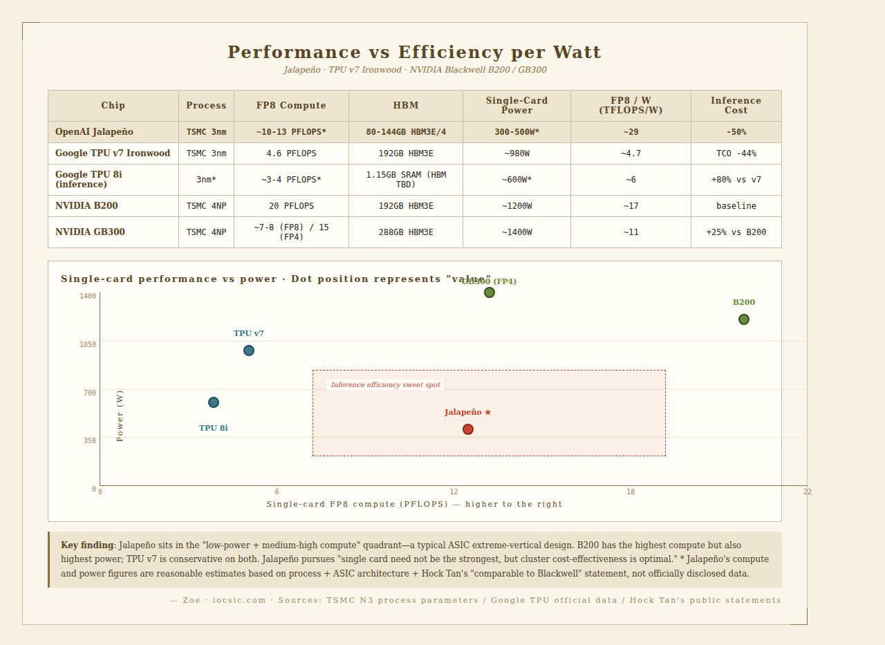
| Chip | Process | FP8 Compute | Memory | Single-Card Power | Interconnect |
|---|---|---|---|---|---|
| OpenAI Jalapeño (est.) | TSMC 3nm | ~10-13 PFLOPS | 80-144GB HBM3E/4 | 300-500W (est.) | Broadcom Tomahawk |
| Google TPU v7 Ironwood | TSMC 3nm | 4.6 PFLOPS | 192GB HBM3E | ~980W | OCS Jupiter 32Tbps |
| Google TPU 8i (inference) | Est. 3nm | Est. 3-4 PFLOPS | 1.15GB on-chip SRAM (main HBM undisclosed) | Est. 600W | Same |
| Google TPU 8t (training) | Est. 3nm | Est. 12 PFLOPS | Est. 192GB+ HBM3E | Est. 980W | Same |
| NVIDIA B200 | TSMC 4NP | 20 PFLOPS | 192GB HBM3E | 1200W | NVLink 5.0 1.8TB/s |
| NVIDIA GB300 | TSMC 4NP | ~7-8 PFLOPS (FP8 est.) / 15 PFLOPS FP4 | 288GB HBM3E | ~1400W | NVLink 5.0 |
Key Observations
- Jalapeño Single-Card Compute May Exceed TPU v7 Ironwood If the estimate is correct (10-13 PFLOPS FP8), Jalapeño's single-card compute is 2-3x Ironwood's. But ASIC vs ASIC needs a discount—TPU also has to accommodate VPU (vector processing unit) and other general-purpose parts, with die area not entirely systolic array.
- HBM Is Jalapeño's Potential Weakness
TPU Ironwood has 192GB HBM3E, 7.4 TB/s bandwidth. If Jalapeño has 80-144GB, 3-4 TB/s bandwidth:
- Large model inference (70B-200B parameters) requires HBM to hold weights + KV Cache
- 144GB just fits 70B FP16 weights (140GB), with little KV space
- This means Jalapeño must combine with model sharding or quantization to serve large models
- Speculation: Jalapeño serves GPT-5.3-style mixed-precision + MoE expert-sharded models, with single cards holding only partial experts
- Single-Card Power Is Jalapeño's Clear Advantage
- ASIC energy efficiency is 2-3x GPU.this is industry consensus
- 300-500W TDP allows simpler cooling (air cooling or light liquid cooling)
- This is likely the main source of Jalapeño's 50% inference cost reduction.not just cheaper chips, but also electricity savings
- Cluster Scalability Is Jalapeño's Open Question
TPU Ironwood clusters support 9,216 cards, 42.5 EFLOPS aggregate compute. How far can Jalapeño's Tomahawk network scale? OpenAI hasn't disclosed, but the 10GW data center target implies needing millions of cards.
Performance Per Watt: The Real Battle
| Dimension | OpenAI Jalapeño | Google TPU v7 Ironwood | NVIDIA B200 |
|---|---|---|---|
| Single-card FP8 compute | ~10-13 PFLOPS | 4.6 PFLOPS | 20 PFLOPS |
| Single-card power | 300-500W | 980W | 1200W |
| FP8 compute per watt (TFLOPS/W) | ~29 | ~4.7 | ~17 |
| Inference cost (relative) | 50% | 44% TCO advantage | Baseline |
If Jalapeño truly achieves ~29 TFLOPS/W (theoretical range 20-43 TFLOPS/W, depending on actual power and compute), it will be the most energy-efficient AI accelerator in history. But this is single-card paper numbers; real "watts per useful throughput" in actual inference workloads will be discounted.
6. Physical Chip Analysis: 3nm, Die Size, Transistor Count
Die Size and Transistor Count
Although OpenAI hasn't released die photos or detailed physical dimensions, combining known parameters we can infer:
- Process: TSMC N3 (same generation as Apple M4)
- Transistor count: Not disclosed. Considering 3nm density and small team design capability, estimated at 50-150 billion transistors (NVIDIA Blackwell B200 is ~208 billion, dual-die)
- Die size estimate: ~600-900mm² (single die, much smaller than B200's 1600mm²)
- Packaging: Speculated to use CoWoS-S or CoWoS-L advanced packaging, with HBM and compute die connected through silicon interposer
Thermal Design
Combined with 3nm process energy efficiency and ASIC architecture's low power characteristics:
- Estimated TDP: 300-500W (far below Blackwell's 1200W)
- Cooling solution: Possibly air cooling + partial liquid cooling, or full liquid cooling
- This means OpenAI's data center cooling costs may be only 1/2-1/3 of Blackwell clusters
HBM and Memory Hierarchy
- HBM3E (estimated 6-8 stacks)
- Total capacity estimate: 80-144GB
- Bandwidth estimate: 3-4 TB/s
Critical Physical Bottleneck: HBM accounts for 30-40% of AI ASIC total cost. Hock Tan has publicly stated that HBM squeezes Broadcom's custom AI chip margins below those of other product lines like network switches.
"AI Designs AI Chips" . The Real Substance
OpenAI's public narrative is "GPT models participated in chip design".but this is PR framing that needs to be split into two levels:
- ✅ Reality: AI participated in logic circuit routing optimization, thermal performance management, power prediction and other EDA steps. These tasks traditionally require weeks of engineering team iteration; AI can complete them in hours
- ❌ Misleading framing: This doesn't mean "AI designed the chip." The most critical front-end architecture definition (systolic array choice, memory hierarchy design, ISA definition) is still done by Richard Ho's team
Industry Progress on AI-Assisted Chip Design
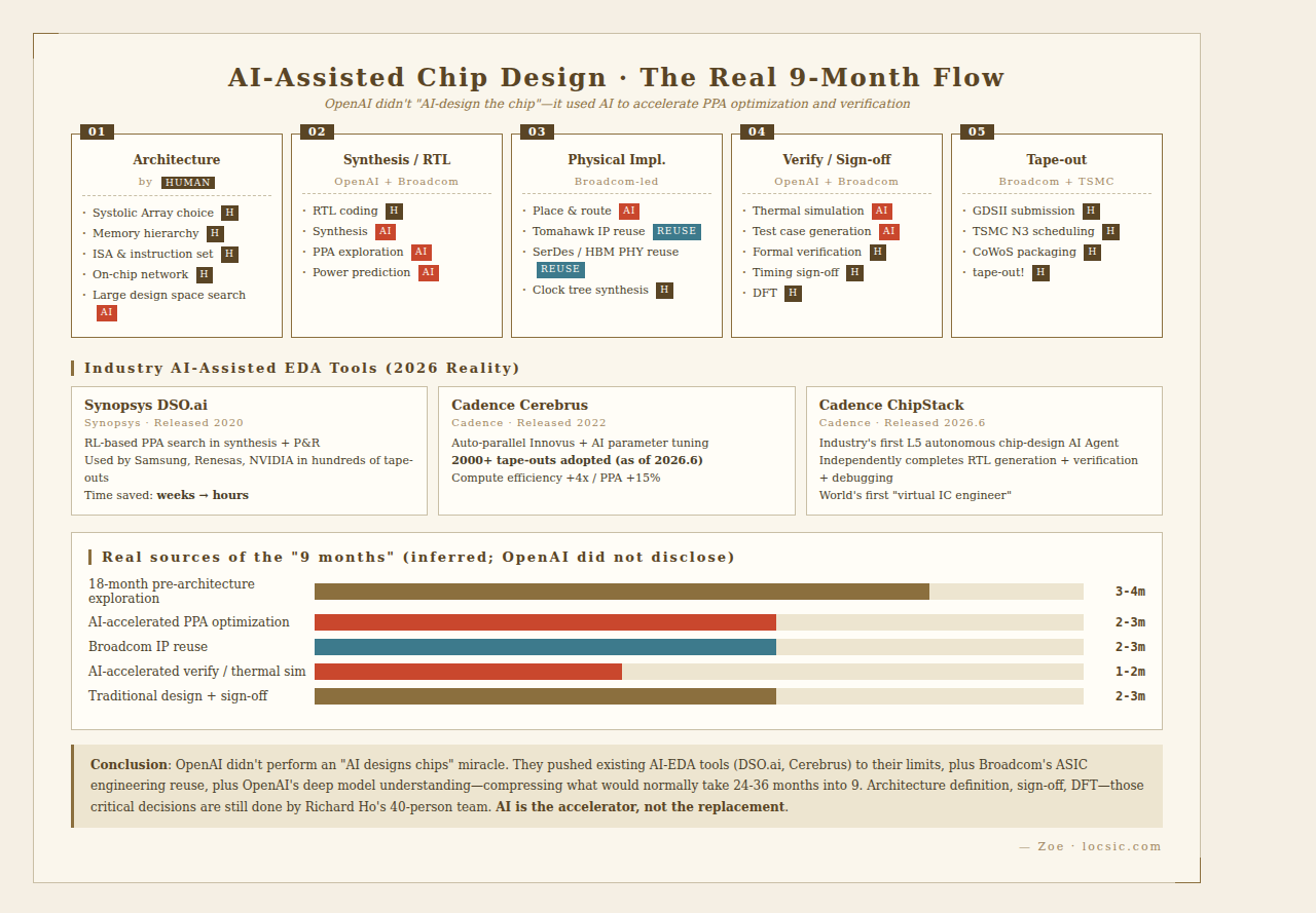
This part is very clear by 2026.AI-assisted chip design is not OpenAI's invention but a paradigm shift the entire EDA industry has been undergoing for the past two years:
- Synopsys DSO.ai (Design Space Optimization AI)
- Released 2020, industry's earliest AI-assisted EDA tool
- Uses reinforcement learning to search PPA optimum in chip synthesis and place-and-route
- Has helped Samsung, Renesas, NVIDIA complete hundreds of tape-outs
- Measured: Compared to manual work, compresses engineering time from weeks to hours, achieves 10-20% additional optimization in power, performance, area
- Cadence Cerebrus
- Released 2022, competing with DSO.ai
- Automatically parallel-runs Innovus physical implementation flow, AI adjusts parameters
- Key data: As of June 2026, adopted by over 2,000 chip tape-outs
- Compute efficiency +~4x
- Turnaround time -~2x
- PPA improvement +~15%
- Cadence ChipStack (Released 2026, industry's first L5 autonomous chip design AI Agent)
- Released June 2026, world's first "virtual IC design engineer"
- EDA autonomy classification (analogous to autonomous driving L1-L5):
- L1-L3: AI as tool assistance (current state)
- L4: AI can understand goals, autonomously call tools
- L5: AI can independently complete RTL generation, verification planning, formal verification, debugging, convergence
- Cadence's "Mental Model" addresses LLM hallucination problems in chip design
- Siemens Celus + Cadence Allegro X AI
- Focus on PCB-level design
- AI automatically generates schematic drafts, place-and-route drafts
- China EDA Progress
- Shanghai Peifeng Tunan Semiconductor (headquarters moved to Zhangjiang in 2026)
- Empyrean Technology, Primarius Technologies (listed companies) accelerating AI-native EDA
Conclusion: The "real substance" of OpenAI's 9-month tape-out is "3-4 months of pre-architecture exploration by the OpenAI + Broadcom team + 2-3 months of AI-accelerated PPA optimization + 2-3 months of Broadcom IP reuse + 1-2 months of AI-accelerated verification and thermal simulation".not "AI designed the chip from start to finish."
7. Software Adaptation: Vertical Integration Advantages and Ecosystem Lock-in Costs
Advantage: OpenAI Is Making a Chip for Itself
Jalapeño's biggest software advantage is no ecosystem migration problem.it doesn't need to sell externally, only adapt to OpenAI's own models:
- Model adaptation range: Verified with GPT-5.3, Codex, Spark
- Forward compatibility with model iterations: Richard Ho states "it will adapt well to all future versions of LLMs"
- Inference framework: OpenAI's own inference stack (likely Triton-based open-source compiler or proprietary engine)
- MRC protocol groundwork: In 2025-2026, OpenAI introduced MRC (Multi-Path Reliable Connection) protocol at the model layer, working with AMD, Broadcom, Intel, NVIDIA, Microsoft on multi-chip high-speed communication optimization
The Gap with NVIDIA's Ecosystem
NVIDIA's CUDA moat is not just the programming language, but:
- 500+ optimized libraries (cuBLAS, cuDNN, TensorRT, TensorRT-LLM)
- Millions of developer ecosystem
- Complete training → inference → deployment toolchain
In contrast, Jalapeño's software stack is a vertical stack customized for OpenAI.an advantage (extreme optimization) and a disadvantage (not general-purpose, cannot capture external ecosystem dividends).
The Real Bet on Software Adaptation
Jalapeño doesn't need global developers writing CUDA code, but it must solve:
- Toolchain for migrating models from H100 to Jalapeño
- Inference optimization (quantization, KV Cache reuse, continuous batching)
- Integration with OpenAI's existing inference infrastructure
- Cluster scheduling (Tomahawk interconnect low-latency routing)
This is Jalapeño's real risk.the hardware tape-outped on time, but can the software be polished before large-scale deployment by end of 2026? Historically, hardware delivery is easy; software ecosystem maturity takes 2-3 years.
8. Horizontal Comparison: AI ASIC Battlefield
Flagship ASIC Specifications Comparison
| Dimension | OpenAI Jalapeño | Google TPU 8i | Google TPU 8t | AWS Trainium3 | AWS Inferentia2 | NVIDIA B200 | Microsoft Maia 200 |
|---|---|---|---|---|---|---|---|
| Positioning | Inference ASIC | Inference ASIC | Training ASIC | Training ASIC | Inference ASIC | General GPU | General inference |
| Process | TSMC 3nm | Est. 3nm | Est. 3nm | TSMC 3nm | 5nm | TSMC 4NP | Est. 5nm |
| Compute (est./conf.) | ~10-13 PFLOPS | ~3-4 PFLOPS | ~12 PFLOPS | ~2.5 PFLOPS/card (source "2.52 EFLOPS" likely PFLOPS, per 144-chip cluster arithmetic) | Lower | 20 PFLOPS | Lower |
| Memory | HBM3E/4 (80-144GB) | 1.15GB on-chip SRAM (main HBM undisclosed) | Est. 192GB+ HBM3E | 144GB HBM3E | Lower | 192GB HBM3E | Higher |
| Interconnect | Tomahawk | OCS Jupiter 32Tbps | Same | Custom | Custom | NVLink 5.0 (~1.8TB/s) | Est. Ethernet |
| Power | 300-500W | Est. 600W | Est. 980W | Higher | Lower | ~1200W | Higher |
| Cost advantage | ~50% vs GPU | 60-70% vs GPU | 40-50% vs GPU | ~50% vs H100 | ~80% vs H100 | Baseline | Est. 30% |
| Availability | OpenAI internal only | External sales | External sales | AWS cloud | AWS cloud | Industry-wide | Azure internal |
| Training capability | ❌ | ❌ | ✅ Primary | ✅ Primary | ❌ | ✅ | ❌ |
| Developer ecosystem | None (proprietary) | Open (JAX/XLA) | Open | Neuron SDK | Neuron SDK | CUDA ecosystem | Est. closed |
Key Judgments
- Google TPU: Most Mature ASIC Paradigm
Google has accumulated 10 years of ASIC experience since TPU v1 (2016). TPU 8i (inference) / 8t (training) correspond to OpenAI's current path and future direction.
Key differences:
- Ecosystem openness: In 2026, Google announced external sales of TPU, partnering with Blackstone to establish a $25 billion AI cloud computing company
- Software maturity: JAX + XLA compiler + TensorFlow deep coupling
- Cluster capability: TPU v7 single Pod 4,096 cards, v7 Ironwood cluster can reach 9,216 cards, 42.5 EFLOPS
- Power cost: TPU v7 single-chip 980W
- Inference cost advantage: TCO 44% lower than GB200
- AWS Trainium: Largest-Scale ASIC Deployment on Cloud
- Trainium3 FP8 compute est. ~2.5 PFLOPS/card (source "2.52 EFLOPS" likely PFLOPS, per 144-chip cluster arithmetic), 144GB HBM3e
- Trainium3 vs Trainium2: performance +30-40%, power -40%
- AWS's biggest advantage: bundled with cloud services, developers don't buy chips, they rent
- Disadvantage: High Neuron SDK migration cost; Cohere/Stability AI report Trainium1/2 underperforming H100 in some scenarios
- Microsoft Maia 200: Most Underrated Competitor
Maia 200 released early 2026, two-plus years after Maia 100. Microsoft's special position:
- Simultaneously OpenAI's largest investor
- Azure also massively deploying NVIDIA GPUs
- Dual identity: both chip player and OpenAI's compute supplier
- NVIDIA Blackwell: Defensive Posture, but Ample Ammunition
- MLPerf 6.0 training: all 7 categories #1
- GB300 NVL72 vs GB200: training speed +1.6x
- Single-chip power 1200W, next-gen Rubin estimated 2300W
- Biggest moat: CUDA ecosystem + full-stack software (TensorRT-LLM, NeMo, Megatron)
- 8,192-GPU cluster has verified DeepSeek-V3 671B training
- OpenAI Jalapeño's Unique Positioning
Jalapeño is the only vertical ASIC in the table that from day one serves only one model family (GPT) and one workload (LLM inference). This is its biggest advantage.extreme vertical.and its biggest limitation.no external sales, unable to amortize R&D costs.
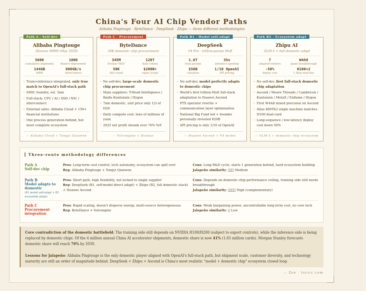
9. Chinese Vendor Self-Developed Chip Panorama
China's AI chip battlefield in 2026 shows three parallel paths: "national team + internet giants + model companies."
1. Alibaba Pingtouge: The Only "Full-Stack Self-Development" Aligned with OpenAI's Path
Latest release: Zhenwu M890 (May 20, 2026, at Apsara Conference)
| Spec | Zhenwu 810E (2024) | Zhenwu M890 (May 2026) | Zhenwu V900 (2027Q3 roadmap) |
|---|---|---|---|
| Process | Undisclosed | Est. 5nm | Est. 3nm |
| HBM | 96GB HBM2e | 144GB HBM | 216GB |
| Inter-chip interconnect | 700 GB/s | 800 GB/s | 1200 GB/s |
| Relative performance | 1x (baseline) | 3x | 9x |
| Use case | Train-inference integrated | Train-inference integrated + Agent optimized | Train-inference integrated |
Key Facts:
- Manufacturing: SMIC
- Cumulative shipments: 560,000 chips (as of May 2026)
- Financial industry deployment exceeded 100,000 cards, covering 150+ institutions
- Self-developed ICN Switch 1.0 interconnect chip, can build 64-128 card super-nodes
- Bundled with Alibaba Xuantie RISC-V CPU, Yitian Arm server, Zhenyue SSD controller, Panmai SmartNIC
- Roadmap: "One generation per year" iteration (same as OpenAI's plan)
Comparison with OpenAI's Path:
| Dimension | OpenAI Jalapeño | Alibaba Pingtouge Zhenwu |
|---|---|---|
| Positioning | Pure inference | Train-inference integrated |
| External sales | ❌ OpenAI internal only | ✅ Alibaba Cloud + enterprise customers |
| Foundry | TSMC 3nm | SMIC (est. 5nm) |
| Ecosystem | Proprietary (self-use only) | Pingtouge + Alibaba Cloud |
| Process gap | 3nm (leading) | Est. 5nm (one generation behind) |
2. ByteDance: Buy-Buy-Buy + Some Self-Development
ByteDance's approach is not relying on self-development, but large-scale procurement of domestic chips:
The 50,000-chip procurement in June 2026:
| Supplier | Quantity | Use Case | Process |
|---|---|---|---|
| T-Head Intelligence Zhikai MR-V100/MR-V100x | ~32,000 | Inference main force | 7nm |
| Baidu Kunlunxin P800 | 15,000 | Video understanding, recommendation | Est. 7nm |
| Hygon DCU K100ai | 3,000 | Edge moderation | - |
Why isn't ByteDance buying H100/H200?
- H20 backdoor incident (end of 2025) increased compliance risk
- H100/H200 not in China's export control exemption range
- Domestic inference chips are now "usable," and unit price is only 1/3 of H20 (Zhikai 20,000 yuan vs H20 ~60,000 yuan)
ByteDance's Compute Bill:
- 2026 AI infrastructure capex: 200-700 billion yuan (different accounting)
- Doubao MAU 345-368 million
- Daily Token calls 120 trillion
- Daily compute cost tens of millions of yuan
- ByteDance 2025 net profit shrank over 70% YoY
3. DeepSeek: Model + Domestic Chip Closed Loop (Not the OpenAI Path)
Latest milestone: DeepSeek V4 Pro (April 2026)
- Total parameters: 1.6 trillion (MoE)
- Actually activated: ~5-8%
- World's first trillion-parameter large model with full-stack adaptation to Huawei Ascend chips
- Inference speed reaches 35x of the initial Ascend migration baseline (DeepSeek's claim, comparison baseline is the early Ascend port version, not H100 or other model comparisons)
DeepSeek's Distinctiveness:
DeepSeek doesn't self-develop chips, but lets models perfectly adapt to domestic chips. This route is smarter than self-developing chips:
- The model company directly controls the full training-inference stack
- Holds the choice of "which operators to ASIC hardcode, which to use general compute"
- Collaborates with Huawei Ascend, Cambricon, Hygon, Moore Threads, MetaX, etc.
DeepSeek V4 on Huawei Ascend key data:
- Through PTX operator layer rewrite + communication layer optimization
- API pricing is only 1/10 of OpenAI
Valuation:
- June 2026: completed first external financing round of 50 billion yuan (~$7.4 billion)
- Post-money valuation over $50 billion (soared from $10 billion to $50 billion in two months)
- National Big Fund led investment, Tencent, Alibaba, CATL, JD, NetEase followed
- Founder Liang Wenfeng personally invested 20 billion yuan
4. Zhipu AI: Deep Adaptation with Domestic Chip Clusters
Latest action: GLM-5 + Full Domestic Chip Adaptation (Feb 2026)
| Domestic Chip | Adapted | Performance |
|---|---|---|
| Huawei Ascend | ✅ | First implementation of W4A8 mixed-precision quantization, single Atlas 800TA3 machine matches H100 dual-card |
| Moore Threads | ✅ | - |
| Cambricon | ✅ | - |
| Kunlunxin | ✅ | - |
| MetaX | ✅ | - |
| Enflame | ✅ | - |
| Hygon | ✅ | - |
Zhipu's Special Contribution:
- First implementation of W4A8 quantization (weights 4-bit, activations 8-bit) on Ascend.this is an industry breakthrough
- In long-sequence, low-latency scenarios, deployment cost reduced 50%
- Zhipu itself doesn't self-develop chips, but as the "model layer," it promotes "model-chip" co-design
5. Overall Domestic Chip Landscape
Domestic AI chip shipments (IDC 2025 stats, includes NVIDIA China shipments + Huawei/Alibaba partial self-use estimates):
- China AI accelerator annual shipments: 4 million cards
- Domestic combined: 1.65 million cards, market share 41%
- Morgan Stanley predicts 2030 domestic share 76%
- Note: 1.65M domestic includes Huawei self-use Ascend + Alibaba self-use Zhenwu; excluding self-use, pure commercial shipments are ~1.2M
9 Domestic AI Chips Receiving National Security Certification Level I (May 26, 2026):
- Huawei HiSilicon Ascend
- Hygon DCU
- Biren Technology
- Vimicro Technology (Starlight Smart 5)
- Pingtouge (Zhenwu series)
- Enflame Technology
- Moore Threads
- MetaX
- Kunlunxin
6. ByteDance vs Alibaba vs DeepSeek vs Zhipu: Path Comparison
| Dimension | ByteDance | Alibaba | DeepSeek | Zhipu |
|---|---|---|---|---|
| Self-developed chip | ❌ (rumors only) | ✅ Zhenwu series (2 generations) | ❌ | ❌ |
| Main strategy | Procurement + integration | Full-stack self-development | Model adapts to domestic | Model adapts to domestic |
| Process | 7nm domestic | Est. 5nm | Domestic | Domestic |
| Train-inference integrated | ✅ (buy GPU) | ✅ Zhenwu | ✅ Ascend | ✅ Ascend etc. |
| Direct OpenAI equivalent | Not directly | Full-stack path similar | Model path similar | Model path similar |
| OpenAI Jalapeño equivalent degree | Low | Medium (path similar, process behind) | High (path complementary) | High (path complementary) |
| Current compute scale (different calibers) | 50K+ this round | 560K cumulative shipments | Est. 10K cards | Est. 1K-10K cards |
7. Three Routes' Methodological Differences
Abstracting from the four domestic strategies, three completely different methodologies emerge:
Route A: Self-Developed Chips (Alibaba Pingtouge)
- Closest to OpenAI's path
- Advantages: Long-term cost control, technology autonomy
- Disadvantages: Long R&D cycle, one generation behind at start, ecosystem building difficult
Route B: Models Adapt to Domestic Chips (DeepSeek, Zhipu)
- Don't touch hardware, let models adapt actively
- Advantages: Short path, high flexibility, not locked to single supplier
- Disadvantages: Depends on domestic chip performance ceiling, training side still needs breakthrough
Route C: Large-Scale Procurement + Limited Self-Development (ByteDance)
- Treat compute as commodity procurement
- Advantages: Rapid scaling, doesn't disperse energy
- Disadvantages: Weak bargaining power, long-term cost uncontrollable
Key Judgments:
- Alibaba Pingtouge is the only domestic player comparable to OpenAI's full-stack self-development path.but still one process generation behind
- DeepSeek + Zhipu represent the "model layer descent" path.more realistic than hard chip-making, rapidly forming "domestic model × domestic chip" ecological closed loop
- ByteDance follows the "NVIDIA path".large-scale procurement + limited self-developed special-purpose chips
- Core contradiction of the domestic battlefield: Training side still depends on NVIDIA H100/H200, inference side is being replaced by domestic chips
- OpenAI Jalapeño's "extreme vertical integration of software and hardware" play.only Alibaba Pingtouge is attempting domestically, but shipment scale, customer diversity, and technology maturity are still an order of magnitude behind
10. Conclusion: The Next Form of an AI Company Is an "AI Full-Stack Company"
Jalapeño's Coordinates in Industry History
Looking at Jalapeño in historical context, the question "do AI companies need self-developed chips?" has traced a clear curve over the past three years:
- 2023: OpenAI, like most AI labs, only cared about models. Compute was a procurement target.
- 2024: Compute prices and supply began to bother model companies. Anthropic and Meta internally began discussing the feasibility of self-developed chips.
- 2025: Google began selling TPU externally, turning "self-developed chips" into a commercial product.
- June 2026: OpenAI closed this loop with Jalapeño. The first AI lab with a valuation over $100B took the field personally.
This is not an endpoint. It is one coordinate point on the timeline.
Five Hard Metrics for Jalapeño's Success
To assess whether an inference ASIC truly "works," five observable hard metrics over the next 18 months:
- First deployment timing: Does OpenAI actually launch by end of 2026, and can scale reach GW level
- Energy efficiency delivery: Is Hock Tan's "50% inference cost reduction" verified in 2027 financial reports
- Software ecosystem maturity: Is native PyTorch / Triton support for Jalapeño demo-level only, or has it entered daily training pipelines
- HBM and capacity: Can HBM4 and TSMC N3 capacity stably supply OpenAI's 10GW roadmap in 2027-2028
- Second-generation iteration pace: Can OpenAI's promised "one generation per year" be delivered.if no second-generation by 2028, the self-developed chip project becomes a capital arbitrage rather than technological evolution
Two Observations on Industry Evolution
Observation One: Self-developed chips have shifted from "differentiated advantage" to "infrastructure necessity." Google TPU's 10-year accumulation, AWS Trainium's 3 generations, Microsoft Maia, Meta MTIA, now OpenAI Jalapeño.the major AI companies have all entered. Those still on the sidelines (like Anthropic) will be constrained by supply security and cost structure.
Observation Two: Model-chip coupling will go deeper. Jalapeño, as a "designed only for GPT series" vertical ASIC, essentially bets that OpenAI's model architecture will remain in the Transformer + MoE paradigm. If Transformer is replaced by a new architecture (e.g., Mamba / SSM class), all of Jalapeño's optimizations become obsolete instantly. This is OpenAI's self-developed path's biggest hidden bet.a bet on their own model architecture stability.
Indirect Significance for the Chinese AI Industry
Jalapeño is a stress test case. It proves "AI companies can build chips" is engineering-feasible, but at a high cost for small companies: 40-person core team + Broadcom's hundreds-strong team + hundreds of millions in tape-out costs.
China's most realistic response is not to imitate this path (except Alibaba Pingtouge), but the opposite: let domestic chips adapt to mainstream models, rather than let models adapt to a single chip. DeepSeek V4 + Ascend, Zhipu GLM-5 + domestic chips are walking this path. This is China's realistic answer to export controls.
Summary
OpenAI made Jalapeño in 9 months. Treating it as a defining moment when an AI company challenges NVIDIA is an overreach; treating it as the latest coordinate point in the "model + self-developed chip" full-stack paradigm is closer to the truth.
The real value of this Mexican pepper Jalapeño is not in its compute numbers, but in confirming a trend: the competitive unit of the AI industry is upgrading from a single model to the entire stack of model + chip + data center + interconnect + scheduling. Once this upgrade completes, the reshaping of industry structure will not be subject to any single company's will.
Appendix A: Key Timeline
- End of 2023: Richard Ho joins OpenAI, forms chip team
- Mid-2024: OpenAI and Broadcom begin secret joint development
- October 2025: Partnership publicly disclosed, 10GW deployment target
- June 24, 2026: Jalapeño officially released
- End of 2026: First deployment online
- 2027: Scaled deployment
- First half of 2028: Full deployment, 1-3GW single cluster
- 2028: Next-generation Jalapeño released
- 2029: 10GW compute cluster completed
Appendix B: Glossary
- ASIC (Application-Specific Integrated Circuit): A chip customized for a specific use case
- HBM (High Bandwidth Memory): 3D-stacked DRAM
- MoE (Mixture of Experts): A model architecture with large total parameters but only a fraction activated per token
- PFLOPS / EFLOPS: PetaFLOPS / ExaFLOPS (10^15 / 10^18 floating-point operations per second)
- Systolic Array: Data flows regularly through processing elements like blood
- TDP (Thermal Design Power): Determines cooling requirements
- Tape-out: Submitting chip layout data to the foundry for manufacturing
- W4A8: Mixed precision with 4-bit weights and 8-bit activations
Appendix C: References
(See the actual published version for full references)