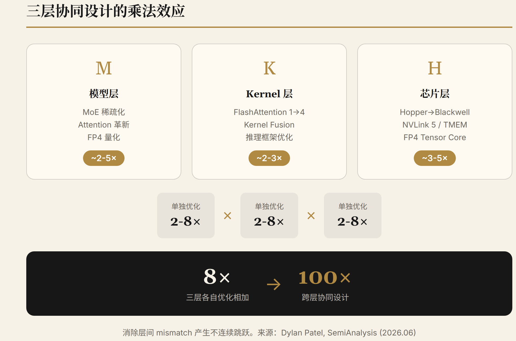
In late June 2026, SemiAnalysis founder Dylan Patel made a bold claim on Sequoia Capital's Training Data podcast: AI efficiency has improved by far more than 30x over the past three years, but hardware's contribution is only the tip of the iceberg. The real 100x leap comes from the co-optimization of three layers — model, kernel, and chip. Improving any single layer in isolation yields only 2–8x; only when all three layers are optimized simultaneously does the multiplicative effect kick in.
This is not idle speculation. DeepSeek's model architecture is tailor-cut for NVIDIA Hopper's matrix units, then re-tuned for Blackwell in V4. NVIDIA itself used the phrase "extreme co-design" in its official Rubin platform press release. Google's open-source Gemma models made architectural choices that differ from GPU-oriented models because of the TPU's distinct shape. Hardware-software co-design is no longer "companies that do it well are more efficient" — it has become "companies that don't do it will gradually lose competitiveness."
This article first decomposes the core arguments from Dylan Patel's interview, then surveys the technical directions within each of the three layers — model, kernel, and chip — and finally analyzes concrete cross-layer co-design practices and their industry implications.
I. Core of the Interview: Why the 100x Lives in Co-Design
1.1 A Counterintuitive Set of Numbers
Dylan Patel directly pushed back against the host's claim that "compute improvements over the past three years mainly came from hardware." His decomposition works as follows:
- Hardware layer: From Hopper to Blackwell, under DeepSeek's optimal deployment conditions, system-level performance improved roughly 30x. This number needs unpacking: single-chip compute increased about 3–5x (FP4/FP8 tensor core, HBM3e bandwidth expansion); NVLink 5 connects 72 GPUs into a shared memory domain, improving communication efficiency about 2–3x; FP4 quantization doubles the data throughput under the same bandwidth, contributing another 2–3x. Multiplied together, these land in the 30x range. The 30x is the combined result of hardware system + quantization format + deployment optimization — not a single-generation jump in chip architecture.
- Model layer: Three years ago, the benchmark was GPT-4. Today, a Qwen model with 27B total parameters and 2B active parameters can surpass it. The compute cost per unit of intelligence has dropped by more than an order of magnitude.
- Co-design layer: FlashAttention iterating from v2 to v4, continuous optimization of inference frameworks (vLLM, SGLang, TensorRT-LLM), quantization advancing from FP16 to FP4 — each of these improvements individually looks like a 2x-level incremental gain. But when they act on the same technology stack, the multiplicative effect far exceeds simple addition.
The key claim: "The real breakthrough innovation is when you leapfrog a few layers — instead of being multiplicative to 8×, it's actually 100×." When optimizations happen synchronously across layers, eliminating the mismatches between them produces discontinuous jumps — not simple 2×2×2=8.
1.2 The DeepSeek Public Case Study
DeepSeek is the best publicly available example of co-design. Dylan Patel noted that DeepSeek V3's expert dimensions and mixing ratios were explicitly designed around Hopper's matrix unit tile sizes and memory hierarchy. V4 further adapted to Blackwell.
What does this mean at the technical level?
DeepSeek V3 employs Fine-Grained Expert Segmentation, with each routed expert containing approximately 33M parameters: the SwiGLU design uses gate_proj + up_proj + down_proj three-layer mappings, yielding parameters = 7168×1536 + 7168×1536 + 1536×7168 ≈ 33M. The choice of 1536 as the intermediate dimension is not arbitrary — Hopper's WGMMA (Warpgroup Matrix Multiply-Accumulate) instructions achieve peak efficiency when the M/N/K dimensions of the matrices are integer multiples of the tile boundaries (16/64/128/256). With 1536 = 128×12 and 7168 = 128×56, the tensor core requires no padding, and utilization can rise from 40–50% (when unaligned) to over 70% (source: SonicMoE paper, arXiv 2512.14080, ablation experiments; SemiAnalysis InferenceX benchmark comparisons).
In V4, DeepSeek introduced Compressed Sparse Attention (CSA) and Heavily Compressed Attention (HCA), abandoning V3's Multi-head Latent Attention (MLA). The design motivation directly targets KV cache pressure — V4 achieved a 73% reduction in per-token inference FLOPs and a 90% reduction in KV cache memory overhead compared to V3.2. Simultaneously, V4's MoE architecture adapted to Blackwell's new features: TMEM (Tensor Memory, 256KB of on-chip dedicated memory per SM) and the Ping-Pong scheduling mechanism allow GEMM epilogue to overlap with the next round of MMA execution. This is particularly important for V4's larger number of finer-grained experts (1.6T total parameters, 49B active).
1.3 Why TPU Runs DeepSeek Poorly
Dylan Patel offered a seemingly paradoxical fact: Google's TPU is "objectively an excellent chip," but it runs DeepSeek inefficiently. The reason is that the model architecture does not match the TPU's topology.
NVLink connects up to 72 GPUs via dedicated switches, forming a shared memory domain. Google's ICI (Inter-Core Interconnect) does not use switches — instead, tokens route through intermediate chips, connecting up to 8,000 chips. The latency and bandwidth characteristics of these two interconnect architectures are fundamentally different. DeepSeek's scattered expert pattern (each token activating 8 routed experts + 1 shared expert) requires frequent all-to-all communication, which can be completed efficiently within NVLink's 72-GPU domain but incurs extra hop latency on the TPU's switchless topology.
The problem is essentially that the model was not optimized for TPU. Google's Gemma series models made different architectural choices because the TPU's systolic array shape differs from the GPU's. Dylan Patel observed a converging trend: Blackwell and TPU are converging at the compute unit level (both support tile-based FP8/FP4 computation; the design philosophies of systolic array and tensor core are drawing closer), but the differences in interconnect topology mean the model architectures they suit remain divergent.
1.4 InferenceX: Empirical Benchmarks
The InferenceX platform, operated by SemiAnalysis, runs automated benchmarks daily on over $50 million in donated hardware, covering the latest chips from NVIDIA, AMD, Google, Amazon, and others. Its core finding: inference cost per unit of quality is dropping approximately 40–60x per year.
This number itself illustrates the power of co-design better than any single-layer optimization. Hardware generational improvements cap out at 5–10x (Hopper → Blackwell → Rubin), but combined with model architecture evolution (from dense to MoE, from 175B to 2B active parameters) and inference framework optimization (FlashAttention, PagedAttention, speculative decoding), the comprehensive efficiency improvement reaches nearly two orders of magnitude per year.
1.5 The Migration of the CUDA Moat
Dylan Patel assessed that the CUDA moat has been "partially eroded," but the real competitive advantage has shifted from programmability to ecosystem synergy. The logical chain is as follows:
Frontier labs can use AI coding tools to write custom kernels for AMD or other chips, lowering CUDA's programmability barrier. But here is the catch: every major Chinese open-source model — DeepSeek, Qwen, Kimi — is co-designed for NVIDIA GPUs. When you build applications on these models, the model's expert shape, attention pattern, and quantization scheme are already deeply coupled with NVIDIA's tensor core and NVLink. Running on non-NVIDIA hardware is not "can't run" — it's "can't run optimally."
The moat has shifted from "CUDA is hard to learn" to "the models are already tailor-made for NVIDIA." Mastery of CUDA is no longer the barrier — the model architecture itself has chosen sides.
II. Where Each Layer Is Heading
2.1 Model Layer: Sparsification, Long Context, and Attention Mechanism Innovation
MoE has become the default choice. DeepSeek V3/V4 and the Qwen series all adopt MoE architectures. The core logic is to achieve large-model-level expressiveness with a small number of active parameters. V3's 671B total parameters activate only 37B (5.5%); V4-Pro's 1.6T activates only 49B (3%). The lower the active parameter ratio, the closer the inference compute cost approaches that of a small model — while model capability remains at the large-model level.
But MoE is not a free lunch. Finer-grained expert segmentation means more all-to-all communication — each token must be dispatched to multiple expert nodes, then aggregated after computation. As the number of experts grows (from V3's 256 routed experts to even more in V4), communication volume grows linearly. This creates a compute-communication tradeoff, whose optimal solution depends on hardware interconnect bandwidth.
The sparse vs. dense divergence. OpenAI's models are sparser (higher expert count, lower per-expert parameter count), while Anthropic's models are relatively denser. This leads the two companies in different hardware directions: OpenAI relies heavily on GPU clusters with high-bandwidth NVLink domains to handle frequent expert switching; Anthropic's denser models can achieve better price-performance on AWS Trainium, as they are less dependent on ultra-low-latency expert communication.
Attention mechanism continues to innovate. From standard Multi-Head Attention to GQA (Grouped-Query Attention), MLA (Multi-head Latent Attention), and further to DeepSeek V4's CSA/HCA — the core goal of attention mechanism optimization is compressing KV cache. V4's replacement of MLA with CSA/HCA reduced KV cache memory overhead by 90%. This is critical for long-context inference: a 1M-token context window using standard attention would consume hundreds of GB of HBM for KV cache alone.
Quantization to FP4 and its boundaries. NVIDIA introduced native FP4 tensor core support (5th generation) starting with Blackwell, and Rubin further enhanced NVFP4 support. FP4 can hold twice the weight data under the same HBM bandwidth compared to FP8, which is decisive for memory-bound inference scenarios (single-card large model deployment). But FP4 is not a panacea: weight quantization in FP4 is generally acceptable (most weights cluster around the center of a normal distribution, and 4-bit exponent + mantissa provides sufficient coverage), but activation quantization is more sensitive — extreme activation values get truncated in FP4, causing information loss in long-tail distributions. NVIDIA's NVFP4 format (Normal Float 4-bit) attempts to mitigate this: it assumes weights and activations follow a normal distribution, using non-uniform quantization with denser sample points near the origin, preserving more useful information than uniform INT4 quantization. In practice, a common deployment strategy is a mixed precision scheme with weights in FP4 and activations retained in FP8 or BF16 — DeepSeek V3's FP8 mixed precision training was a precursor to this approach.
A key architectural decision in Rubin further reinforces this direction: the doubled tensor core width (from Blackwell's 16,384 FP4 MACs/clock to 32,768 FP4 MACs/clock) applies only to FP4 and FP8, while BF16 and TF32 remain the same as Blackwell (source: SemiAnalysis Vera Rubin analysis, February 2026). This means NVIDIA is voting with silicon area — the future mainstream compute workload will migrate to FP4/FP8, and BF16 will gradually be marginalized. If a model team's quantization scheme cannot run efficiently at FP4/FP8, the hardware acceleration they can access will increasingly fall behind.
2.2 Kernel/Runtime Layer: Fusion, Specialization, and AI-Assisted Development
Three generations of FlashAttention evolution. From the first generation in 2022 introducing the IO-aware tiling algorithm, to FA-2 improving parallelism and work partitioning, to FA-3 leveraging asynchronous execution and warp specialization on Hopper to reach 740 TFLOPS (H100 BF16), and finally to FA-4 in 2026 achieving 1,613 TFLOPS on Blackwell (B200 BF16, 71% utilization).
The technical leap in FA-4 deserves elaboration. It is written in CuTeDSL (CuTe Domain Specific Language) rather than traditional CUDA C. The reason is not mere preference — Blackwell's TMEM (Tensor Memory, 256KB dedicated memory per SM) and UMMA (Unified Matrix Multiply-Accumulate) instructions represent an entirely new hardware abstraction layer that CUDA C cannot directly express. CuTeDSL provides tiled tensor abstractions, letting developers precisely control TMEM layout and UMMA dispatch timing. Core innovations include: a fully asynchronous MMA pipeline (complete overlap of computation and data loading), larger tile sizes (leveraging TMEM's 256KB/SM capacity), software-emulated exponential functions (avoiding the hardware exp unit becoming a bottleneck), conditional softmax rescaling (dynamically adjusting numerical range during tile accumulation), and 2-CTA MMA (matrix multiplication across two Cooperative Thread Arrays, breaking through the single-CTA shared memory limit). These features enable FA-4 to reach 1,613 TFLOPS on B200 (BF16, 71% utilization) — 1.3x faster than cuDNN 9.13 and 2.7x faster than Triton.
Kernel fusion is the key lever for inference performance. The decode phase of inference is memory-bandwidth-bound — every unnecessary HBM round trip wastes bandwidth. Kernel fusion merges multiple operators into a single kernel execution, eliminating intermediate result reads and writes. Typical fusion combinations include: attention + rotary embedding + layernorm, and MoE's gate + token dispatch + expert GEMM + combine. The FlashInfer library (led by NVIDIA contributions, incorporating high-performance kernels from TensorRT-LLM) has become the unified kernel backend for both vLLM and SGLang, reducing inter-token latency by 29–69% in batch 8–64 scenarios.
The divergence of inference frameworks. The three mainstream frameworks have taken different paths:
- vLLM: Generality first. PagedAttention manages fragmented KV cache, continuous batching improves throughput, deployment is simple, and it supports the widest range of models. No compilation step required, making it the default choice for most teams.
- SGLang: Prefix reuse and structured generation. RadixAttention provides significant advantages for requests sharing common prefixes (such as agent workflows, RAG pipelines), making it well-suited for agentic scenarios.
- TensorRT-LLM: Compilation first. Compiles models into optimized TensorRT engines, completing kernel fusion, memory layout tuning, and hardware-specific acceleration all at once before execution. Post-compilation throughput is 8–13% higher than vLLM, but compilation takes tens of minutes, and the cost of model changes is high.
AI coding tools are transforming kernel development. Frontier labs have begun using AI to assist in writing custom kernels — given the characteristics of the target hardware (tensor core specs, shared memory size, warp count), AI can generate fused kernels tailored to specific operator combinations. This has, to some extent, lowered CUDA's programmability barrier. DeepSeek's own DeepGEMM (FP8 GEMM kernel library) is a product of this paradigm — optimized specifically for their MoE expert shapes rather than general-purpose GEMM.
2.3 Chip Layer: Low Precision, Large Memory, Interconnect Density
NVIDIA's three-generation evolution. Hopper (H100/H200) introduced the FP8 Transformer Engine and dynamic precision switching. Blackwell (B200/B300) added 5th-generation tensor core with native FP4 support, doubled NVLink 5 bandwidth to 1.8 TB/s, expanded HBM3e to 192–288 GB, and introduced TMEM (256KB on-chip dedicated memory per SM) and UMMA instructions. Rubin (R100) achieves 336B transistors on 3nm process, with HBM4 providing 22 TB/s bandwidth, FP4 compute reaching 50 PFLOPS (5x that of Blackwell), and NVLink 6 doubling again to 3.6 TB/s.
A key architectural decision in Rubin: the doubled tensor core width applies only to FP4 and FP8, while BF16 and TF32 remain the same as Blackwell. This means NVIDIA is making a bet — the future mainstream compute workload will migrate to FP4/FP8, and BF16 will be marginalized. If this bet pays off, the trajectory of model quantization and low-precision training will further accelerate.
Google TPU's differentiation. The core difference of TPU is not in the compute unit (systolic array efficiency at FP8/FP4 is on par with tensor core), but in interconnect topology. ICI's 8,000-chip switchless interconnect suits dense models that require large-scale parameter parallelism, but is unfriendly to MoE's fine-grained all-to-all communication. Google's internal Gemini models are, naturally, fully optimized for TPU — but Google has also begun physically selling TPUs to external customers (including Anthropic), representing a strategic shift.
AWS Trainium's position. Anthropic, as the anchor user of Trainium (over 1 million Trainium2 chips, with a commitment exceeding $100 billion over 10 years), validates the viability of custom ASICs in frontier lab scenarios. Trainium's advantages lie in cost control and supply chain diversification, but the maturity of its software ecosystem (Neuron SDK) remains a catch-up item.
Cerebras and Groq's niche. SRAM-based architectures have extreme advantages in inference speed — Cerebras can achieve near-instantaneous token generation, and SemiAnalysis itself uses them extensively for latency-sensitive tasks. But SRAM's capacity limitations make it difficult to scale to ultra-large model + long-context scenarios. This is a specialized path, not a replacement for general-purpose GPU/TPU clusters.
2.4 GPU Microarchitecture: The Shifting Balance Between Compute Units
The above covers chip-level evolution. Looking further down into the GPU microarchitecture layer, the resource allocation and design tradeoffs among several key hardware units directly determine the real efficiency of a model running on the chip.
Tensor Core: From general-purpose accelerator to AI-specialized engine. When first introduced in Volta (2017), each SM had 8 tensor cores (2 per partition across 4 partitions), supporting only FP16 matrix multiplication. Hopper's 4th generation has 4 tensor cores per SM (1 per partition across 4 partitions), but each tensor core's tile throughput is vastly expanded (supporting larger M/N/K dimensions and FP8), and combined with WGMMA async instructions and TMA pipelines, the overall GEMM throughput is tens of times that of Volta. Blackwell's 5th generation added native FP4/FP6 support, TMEM (256KB/SM dedicated accumulator memory), and UMMA instructions, enabling epilogue to overlap with the MMA pipeline. Rubin doubles the tensor core width to 32,768 FP4 MACs/clock (2x Blackwell), but only for FP4 and FP8.
The direction of tensor core evolution is clear: area and power are increasingly skewed toward low-precision computation, while higher precision (BF16, TF32) no longer receives commensurate hardware resource growth. This means that if model designs insist on using BF16, the hardware acceleration they can obtain will increasingly lag behind FP4/FP8-based approaches.
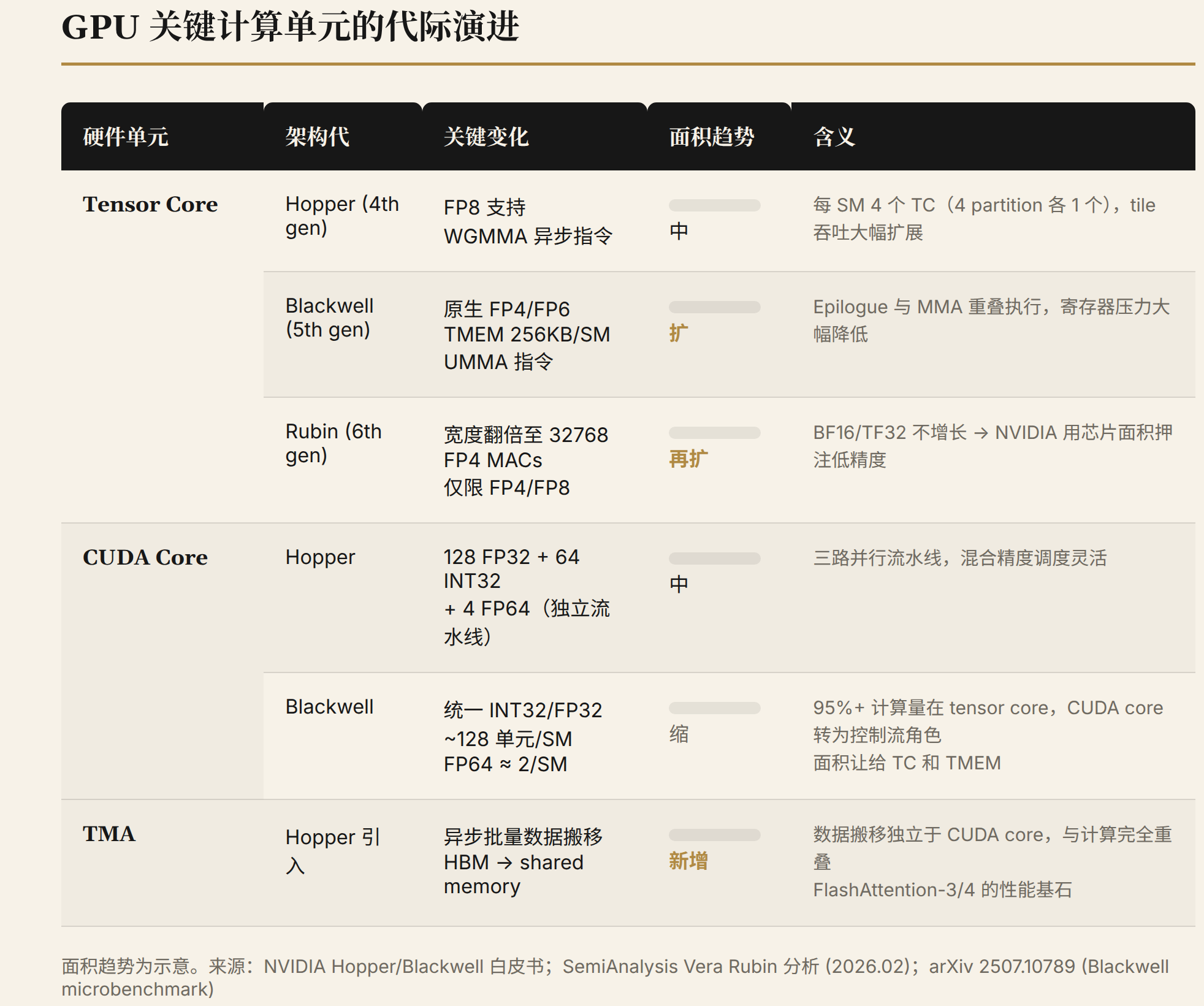
CUDA Core: The contraction of scalar compute units. This stands in contrast to the tensor core's expansion. Hopper's H100 SM has 128 FP32 CUDA cores and 64 INT32 cores — a three-way parallel pipeline (FP32 + INT32 + 4 FP64 units), each with independent execution units. Blackwell merges INT32/FP32 into a unified pipeline (approximately 128 unified units per SM), and reduces FP64 to approximately 2 per SM. CUDA core counts have not grown significantly, but unified scheduling provides more flexibility during mixed precision execution.
This is not CUDA core performance regression — it reflects NVIDIA's bet that AI inference and training no longer depend on general-purpose scalar computation. By the Blackwell era, over 95% of compute workload falls on tensor cores, and CUDA cores are increasingly used for control flow, address calculation, and non-matrix data processing. Although the unified pipeline's single-instruction throughput remains on par with before, the silicon area saved has been reallocated to tensor cores and TMEM.
TMA (Tensor Memory Accelerator): The underestimated data movement engine. Introduced in Hopper, TMA is a dedicated hardware unit for data movement within the SM. In traditional GPU GEMM execution, CUDA cores must participate in data movement — copying from HBM to shared memory before launching tensor core computation. TMA makes data movement independent of CUDA cores: a thread submits a TMA operation (source address, destination shared memory, tile size), and the TMA hardware completes the transfer automatically. The result: data movement and computation can fully overlap, significantly improving GPU utilization.
DPX (Dynamic Programming Accelerator): A niche but important addition. The DPX unit introduced in Hopper provides hardware acceleration for dynamic programming algorithms (such as sequence alignment, shortest path), completing max/min + add + clamp-to-zero in a single instruction. This reflects GPU architecture shifting from "try to be general-purpose" to "identify high-frequency patterns and harden them" — a philosophy shared with the tensor core.
NVLink + NVSwitch: Communication as a chip-level design constraint. This is another main thread beyond the GPU's internal architecture — the inter-GPU communication. NVSwitch is a high-bandwidth switch connecting all GPUs within a rack. Each generation's doubled NVLink bandwidth (4→5→6: 900 GB/s → 1.8 TB/s → 3.6 TB/s per GPU) directly impacts the all-to-all communication efficiency of MoE training and inference. But there is approximately an 18x gap between intra-NVLink-domain bandwidth (H100: 900 GB/s) and cross-node network bandwidth (typical value: 400 Gb/s ≈ 50 GB/s per InfiniBand port) — which is why all distributed training frameworks require hierarchical reduction: first perform reduce-scatter within the NVLink domain, then execute all-reduce across nodes, and finally all-gather within the NVLink domain.
NVLink SHARP: In-switch reduction. Starting from the 3rd generation, NVSwitch supports SHARP (Scalable Hierarchical Aggregation and Reduction Protocol), enabling all-reduce summation operations to be completed inside the switch rather than consuming GPU compute resources. Traditional ring all-reduce requires each GPU to send data, receive data, reduce, then forward — 2(N-1)/N data transmissions. With SHARP, each GPU only needs to send data to the switch once; the switch performs the reduction and broadcasts the result back. NCCL's NVLS algorithm is designed specifically for this topology, and NVLS Tree further uses tree-based fan-out for inter-node communication.
Four collective operation algorithms, each with tradeoffs. NCCL automatically selects based on message size and topology: Ring is suited for large-volume data (all links busy simultaneously, optimal bandwidth); Tree is suited for small messages scaling to large clusters (log(N) hops, optimal latency); NVLS leverages NVSwitch SHARP (reducing transmission rounds); CollNet leverages InfiniBand SHARP (cross-node reduction). The same collective operation (e.g., all-reduce) may use NVLS within the NVLink domain and switch to ring across nodes — NCCL handles this automatically, which is the core implementation of the hierarchical communication described above.
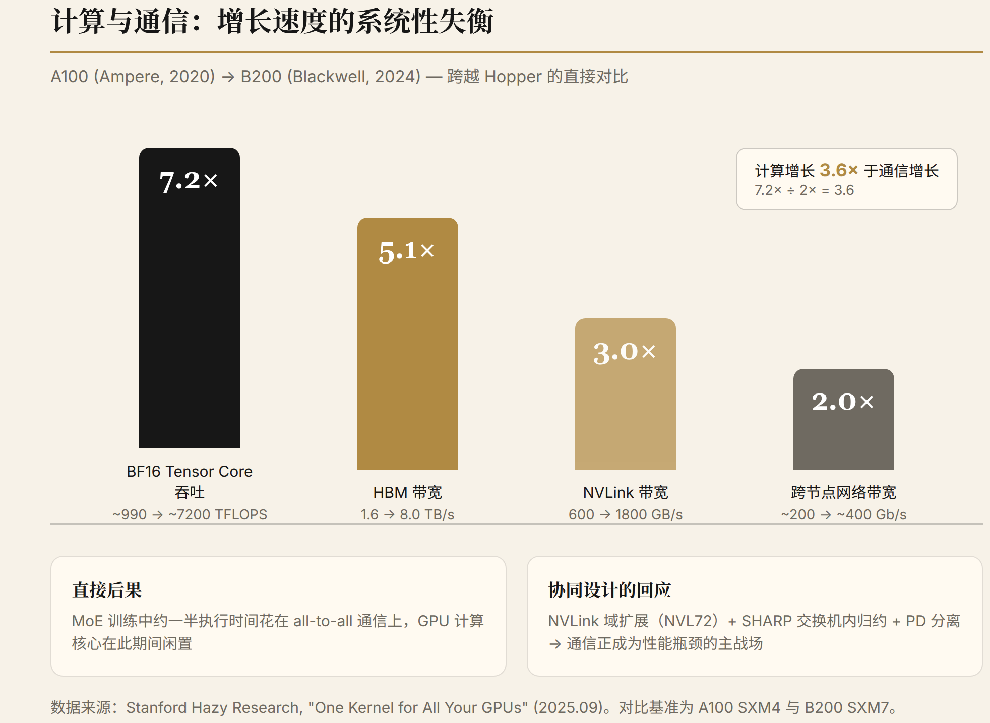
Quantifying the compute-communication tradeoff. Stanford Hazy Research's 2025 measurements (One Kernel for All Your GPUs) show that in the direct comparison from A100 (Ampere) to B200 (Blackwell), skipping Hopper: BF16 tensor core throughput improved 7.2x, HBM bandwidth improved 5.1x, NVLink bandwidth improved 3x, and cross-node network bandwidth improved only 2x. Communication bandwidth growth systematically lags behind compute — in MoE training, approximately half of execution time can be spent on all-to-all communication, with GPU compute cores idle during this period. This explains why communication-structure co-design (NVLink domain expansion, SHARP offload, PD disaggregation) is becoming the primary battleground for performance bottlenecks.
2.5 Two Reverse Paths from Software to Hardware
The above covers what can be done starting from hardware characteristics. Looking in the reverse direction — how software leverages existing hardware features, and where it hints at what the next hardware generation should optimize — is the other half of understanding the complete co-design picture.
2.5.1 Leveraging Hardware: How Software "Borrows" GPU Features
FlashAttention's layered exploitation of TMA and TMEM. FA-3's high performance on Hopper relies on two hardware features: TMA handles asynchronous data movement (Q, K, V tiles from HBM → shared memory), while WGMMA handles asynchronous matrix computation. The independent asynchronicity of these two hardware units is precisely orchestrated by FlashAttention's software pipeline — the three stages of tile loading + softmax computation + result write-back are fully overlapped. FA-4 goes further, using Blackwell's TMEM to replace traditional registers as accumulators, relieving substantial register pressure and enabling larger tile sizes (thanks to TMEM's 256KB/SM capacity). The software design is built directly around hardware features.
DeepSeek MLA as a hedge against the HBM bandwidth wall. The core of Multi-head Latent Attention is compressing KV cache into a low-dimensional latent space (approximately 4–8x compression), where each token stores only the compressed latent vector rather than full KV. This is fundamentally a software-level response to the HBM bandwidth wall — in a reality where HBM bandwidth growth cannot keep pace with the expansion of model context windows, the algorithm reduces per-token HBM read volume. V4's CSA/HCA continues this path.
Speculative decoding fills idle GPU cycles. The decode phase of inference is bandwidth-bound — GPU compute units spend most of their time waiting for KV cache to arrive from HBM. Speculative decoding's approach is to have a lightweight draft model make fast predictions (consuming minimal compute), then batch-verify with the target model (significantly increasing the token output per decode step). This is a software strategy addressing a hardware utilization problem — using the idle SMs during the memory-bandwidth-bottlenecked period for lightweight inference.
MoE expert routing aware of NVLink topology. DeepSeek and Kimi K2.5's expert routing strategies are not purely semantics-based but incorporate hardware topology constraints: tokens are preferentially routed to experts within the same NVLink domain, avoiding cross-domain communication. Intra-NVLink-domain bandwidth at 1.8 TB/s (Blackwell) far exceeds cross-node bandwidth (~100 GB/s), and the model's routing decisions implicitly encode this order-of-magnitude difference.
2.5.2 Reverse-Influencing Hardware: Which Software Patterns Deserve Hardening
Standard patterns continuously emerging in the software layer are providing design directions for the next hardware generation.
Attention mechanisms are standardizing → dedicated attention units. FlashAttention went from academic prototype to standard equipment in every inference engine within four years. The operation sequence of causal multi-head attention + softmax + KV cache has become highly standardized. Groq's LPU has already implemented attention-specific hardware using a SRAM streaming architecture; NVIDIA's approach is to incrementally add hardware support for attention across generations — TMA (data movement) → TMEM + UMMA (matrix accumulation) → the next step may be a complete attention accelerator pipeline. This judgment aligns with Dylan Patel's observation in the interview: when a certain operation pattern remains stable across several generations, it should be in hardware.
PD disaggregation from experiment to product → heterogeneous inference chips. DeepSeek's PDC architecture publicly validated that prefill (compute-intensive) and decode (bandwidth-intensive) require different hardware configurations. NVIDIA's acquisition via Groq 3 LPX validated this direction — a standalone SRAM-based chip dedicated to decode, while the main GPU handles prefill and training. If PD disaggregation becomes the standard deployment mode for inference, next-generation inference hardware will likely move toward chip-level heterogeneity: high compute-density chips (prefill) + high memory-bandwidth chips (decode).
MoE all-to-all communication pattern → SHARP and PXN. MoE's core communication pattern (token dispatch + expert computation + combine) is extremely sensitive to all-to-all latency. NCCL 2.12's PXN (Proxy eXtended NIC) technology reduces cross-node transmission volume by rearranging data placement within the NVLink domain, and NVSwitch's SHARP offloads reduction operations to the switch. These are essentially software-layer pain points being hardened into the next hardware generation. Future NVSwitch may support dedicated all-to-all primitives.
Standardization of FP4 quantization → native tensor core support. FP4 received native tensor core support starting with Blackwell, and Rubin further doubled the tensor core width targeting FP4 rather than BF16. This evolution path is clear: software model teams first validated that FP4 precision is sufficient (DeepSeek V3's FP8 mixed precision training), then NVIDIA software-defined the NVFP4 format, and finally it was hardened into a native path at the hardware level. Software validates first → hardware reinforces second — this is the healthiest co-design rhythm.
III. Key Directions in Co-Design
3.1 Model Architecture Aligned to Hardware Tiles
The SonicMoE paper (2026) provides the most concrete technical implementation of model↔chip co-design: tile-aware token routing. The core idea is to ensure that the number of tokens distributed to each expert by the MoE router is always an integer multiple of the GEMM tile size. On Hopper, this means each expert receives a token count that is a multiple of 128 (the WGMMA tile height); on Blackwell, the tile shape changed (UMMA has different tile configurations), and the optimal token count is adjusted accordingly.
This design produces an interesting hardware-model coupling: token routing is no longer a routing decision determined purely by model semantics, but an engineering problem constrained by hardware tile sizes. SonicMoE measured a 1.86x throughput improvement (86% speedup) on Hopper and Blackwell compared to the traditional ScatterMoE baseline. Token rounding, by eliminating padding waste, contributed approximately 16 percentage points, with the remainder coming from overlap optimization with Blackwell's TMEM pipeline. Model quality degradation was negligible.
3.2 Inference Paradigm and Chip Architecture Shaping Each Other
The rise of reasoning models (OpenAI o-series, DeepSeek R1) has changed the characteristics of inference workloads: from short input → short output generation, to short input → long chain-of-thought reasoning → long output generation. This means the decode phase (memory-bandwidth-bound) becomes the performance bottleneck, rather than prefill (compute-bound).
Cerebras and Groq gained an inherent advantage in reasoning scenarios with their SRAM/streaming architecture — high-throughput sequential token generation perfectly exploits their deterministic execution and low-latency characteristics. This is what Dylan Patel meant on the MatX podcast when he said "reasoning and RL disrupted the hardware roadmap": chips designed for traditional inference (short prompt → short output) need to redesign their memory-to-compute ratio under reasoning workloads (short prompt → long chain reasoning → long output), shifting from ~1:10 toward ~1:20+.
3.3 NVIDIA's "Extreme Co-Design" Strategy
Rubin is the most direct embodiment of NVIDIA using hardware to accommodate model workloads — the complementary direction to DeepSeek's "models accommodating hardware." The official use of the phrase "extreme co-design" signals that this is no longer just GPU iteration, but the design of six chips (Rubin GPU, Vera CPU, NVLink 6 Switch, ConnectX-9, BlueField-4, Spectrum-6) as a single coordinated compute unit.
Specific co-design effects:
- Vera CPU and Rubin GPU share data bidirectionally and coherently, reducing the PCIe transfer bottleneck between CPU and GPU.
- NVLink 6 expands the 72-GPU domain to a larger scale (Rubin NVL72 rack), enabling MoE expert all-to-all communication to complete within a single rack.
- ConnectX-9 and BlueField-4 handle network and storage offload, letting GPUs focus on computation.
- The 3rd-generation Transformer Engine replaces 2:4 structured sparsity with a new sparsity mode, combined with NVFP4 to achieve an effective 50 PFLOPS of FP4 performance.
The result: compared to the Blackwell platform, Rubin claims a 10x reduction in inference token cost and a 4x reduction in MoE training GPU count. These numbers are only achievable under cross-layer co-design — single-chip performance improvement alone could never reach 10x.
3.4 Disaggregated Deployment of MLP and Attention
The MatX podcast discussed a more radical co-design direction: separating the MLP layers and attention layers of a transformer onto different hardware resources. The resource characteristics of the two operator types are fundamentally different — this is not merely an engineering preference:
- MLP layers are compute-intensive. The primary operations are two large matrix multiplications (GEMM), bottlenecked by tensor core FLOPS throughput. During decode with small batch sizes, each token's MLP computation takes only a few hundred microseconds, but requires the SMs to run at full speed during that time.
- Attention layers are memory-bandwidth-intensive. During decode, generating each token requires reading the entire KV cache — for a 128K-context, 671B-parameter-class MoE model, the KV cache can reach tens of GB. The compute volume is modest, but HBM bandwidth is the bottleneck.
When both are executed alternately on the same set of GPUs, resource utilization is inevitably unbalanced: during MLP computation, HBM bandwidth sits largely idle (GEMM data cycles within shared memory / TMEM); during attention computation, tensor cores sit largely idle (only performing dot products without large-scale matrix multiplication). Overall GPU utilization typically reaches only 30–40%.
The logic of disaggregated deployment is to dedicate one set of GPUs to GEMM (which can be configured in a high compute-density mode, even with different voltage/frequency curves), and another set to KV cache management (with larger HBM capacity and lower compute specifications). In theory, utilization of both resource groups can be pushed above 60–70%.
DeepSeek's PDC (Prefill-Decode Disaggregated Serving) architecture is a pioneering case. PDC separates prefill and decode onto different nodes — prefill nodes handle long prompt inputs (compute-intensive), while decode nodes generate tokens sequentially (bandwidth-intensive). According to the DeepSeek V3 technical report (December 2024) and its production deployment data, PDC deployment can achieve over 2x effective throughput improvement compared to mixed deployment. The further separation of MLP/attention disaggregates hardware resources by operator type (compute-bound vs. memory-bound) rather than by phase, providing finer granularity.
The constraining factor is communication overhead: after disaggregation, activations between MLP and attention must traverse NVLink, introducing approximately 5–10 microseconds of additional latency. For latency-sensitive interactive scenarios (such as real-time conversation), this overhead needs to be weighed. But for throughput-prioritized batch inference (reasoning, batch API), the benefits of disaggregated deployment far exceed the communication cost.
3.5 Industry Landscape: Co-Design as Competitive Moat
Dylan Patel's assessment carries several deeper implications for the industry landscape:
NVIDIA's real moat: ecosystem synergy lock-in, not CUDA. When the architectures of mainstream open-source models like DeepSeek, Qwen, and Kimi are all optimized for NVIDIA GPUs, the cost for downstream users choosing non-NVIDIA hardware is not merely rewriting kernels — it's performance degradation at the model architecture level. Jensen Huang's deliberate support of NeoClouds (CoreWeave, etc.) aims to distribute GPUs to as many buyers as possible, not for short-term revenue — "a GPU sold to CoreWeave today will weaken Google TPU and Amazon Trainium competitiveness five years from now."
The calculus of custom ASICs. Google and Amazon invest heavily in developing TPU and Trainium. The core driver is the autonomy that co-design affords, not chip cost (advanced process NRE costs are extremely high). Google can ensure Gemini's architecture perfectly matches the TPU's systolic array shape; Amazon can ensure Trainium's sparse compute capabilities suit Anthropic's dense models. This vertical integration advantage can only be realized when model teams and chip teams work in tight coordination.
The challenge for Chinese AI chips. According to the SemiAnalysis DeepSeek V4 deep analysis (June 9, 2026) report, DeepSeek V4 supported Huawei Ascend 950 deployment on launch day, indicating that co-design has extended beyond the NVIDIA ecosystem. However, the challenge for Ascend is: NVIDIA iterates one architecture generation per year (Hopper → Blackwell → Rubin), and models adjust accordingly. For Chinese chips to keep pace with this co-design cadence, they need synchronized evolution of both model teams and chip teams — not merely single-point performance catch-up.
IV. Conclusion: The Next Phase of Co-Design
Dylan Patel's 100x framework provides a clear model for understanding AI efficiency improvement: what drives cost reduction in AI is the multiplicative effect across model architecture, kernel optimization, and chip design — not the advancement of any single layer.
The corollaries of this framework:
- Model teams cannot focus only on models. Model architecture decisions (how large each expert is, how sparse, which attention mechanism) directly affect how fast the hardware can run. Model teams that ignore hardware tile sizes will lose on inference costs.
- Chip companies cannot look only at FLOPS. Rubin's 50 PFLOPS FP4 figure is only realizable when models actually use NVFP4 quantization and attention patterns are adapted to TMEM scheduling. A chip's competitiveness increasingly depends on the depth of its co-design with the upper software stack.
- The differentiation of inference frameworks is narrowing. FlashInfer, as NVIDIA's flagship unified kernel library, is absorbing high-performance kernels from TensorRT-LLM into vLLM and SGLang, and the kernel quality gap among the three major frameworks is shrinking. Differentiation will increasingly come from scheduling strategies (such as PD disaggregation, prefix reuse) rather than kernels themselves.
- The next 100x may come from more radical architectural changes. Several long-term bets mentioned by Dylan Patel — analog compute (chip physics layer), energy-based models (algorithm paradigm), co-packaged optics (interconnect layer) — each has the potential to disrupt the current co-design paradigm and initiate a new round of multiplicative effects. But they act on different stack layers, with significant differences in timeline and maturity. CPO is closest to deployment (expected before 2030); analog compute and EBMs remain at the basic research stage.
But for at least the next 3–5 years, the dominant force driving AI efficiency improvement will remain the deepening of the current paradigm: finer-grained MoE, more aggressive quantization, deeper kernel fusion, and tighter model-hardware coupling. Dylan Patel's judgment — that inference will become a larger market than oil — if correct, means that whoever pushes this co-design chain to its utmost limit will command the most valuable infrastructure layer of the AI era.
Disclaimer: This article is based on information synthesized from publicly available sources, including: Sequoia Capital Training Data podcast Episode 92 (June 30, 2026, Dylan Patel interview); MatX podcast (April 20, 2026, Clive Chan / Dylan Patel / Reiner Pope discussion); SemiAnalysis DeepSeek V4 deep analysis (June 9, 2026); SonicMoE paper (arXiv 2512.14080); NVIDIA Rubin official technical documentation; and SemiAnalysis Vera Rubin analysis (February 25, 2026). This article does not constitute investment advice. Data herein is current as of July 5, 2026.