
Hot Chips 2026 specialist · Hyperscaler silicon
GPT-5.2's serving workload runs on a Microsoft-designed chip: MAIA 200 already carries GPT-5.2, M365 Copilot, and Foundry. At this Hot Chips, three clouds all brought second-generation custom silicon, and for the first time the training-inference division shows up in the form of the chips: Meta fits recommendation and GenAI into one chip, Microsoft built a systems-grade chip for inference, Google split into two. Generation one was about daring to try; generation two is about what architecture to build. AWS Trainium is absent — the only one of the four majors without a second-generation chip on stage, and the absence itself says something.
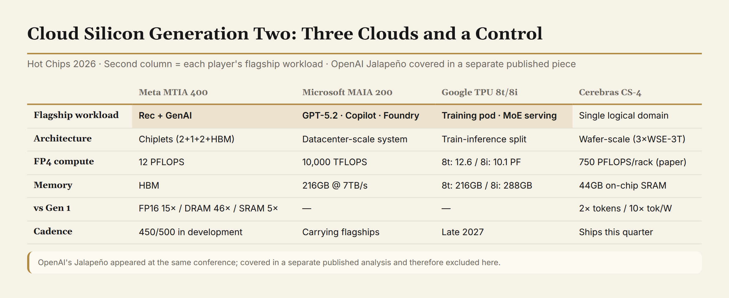
1. Meta: One Chip, Two Workloads
The generations first. MTIA's roadmap was completed at this conference: 200 (2024, inference, 5nm, 0.354 PFLOPS) → 300 (2025, the first DLRM training chip, 3nm plus HBM3E, 1.112 PFLOPS) → 400 (2026+, DLRM inference plus GenAI training). The 300 delivered measurements: GPU parity at competitive TCO on a 150B-parameter DLRM, embedding operators at 1.87×/1.88× (forward/backward) over leading GPUs, 2.2× scale-up bandwidth, full-precision comms that skip FP8 quantization. The 400's dual mandate therefore rests on a chip that has already proven itself in training.
Architecturally, the 400 composes five dies in a 2.5D package: two compute dies (3nm, 1.7GHz) carry the PE arrays and on-chip memory, one SoC (3nm, 1.5GHz) carries the host bridge and control, two I/O dies carry RoCE networking; eight HBM3E stacks provide 288GB at 9.4TB/s, compute-die-to-compute-die runs at 13TB/s, and the scale-up domain organizes over 12TB/s of RDMA. The official motive for chipletization is stated plainly: yield and cost. Advanced-process risk is split across small dies, and control and IO no longer share the yield burden of a large compute die.
The compute body is an 8×6 PE array per compute die with a redundant row: defective rows are masked and replaced at fab time, pressing the yield risk of a large array down to row level. The GPU industry masks compute units through harvesting; Meta pushes the same method to PE granularity. The generational jump has official numbers: the 400's FP16 throughput of 3 PFLOPS is 5× the 300 and 15.4× the 200; GEMM hardware density is 4× over the 300, paired with native MX microscaling formats (16 elements per shared exponent, finer than the OCP standard's 32, with MX4 throughput at 2× FP8).
The dedicated parts show how two workloads coexist: twelve ME collective engines (six per compute die) carry GenAI training collectives, with streaming reduction and hardware semaphores achieving zero-CPU synchronization; HEC and PEC embedding caches pin the recommendation hot tables next to the PEs; the LLC supports in-memory read-reduce-write. At system level, four chips per compute tray and a scale-up domain of 72 ASICs over 8 switches.
The official figures weight the two workloads: against the MTIA 200, 46× DRAM bandwidth and 16× host PCIe bandwidth sit on the recommendation side, SRAM bandwidth at 5× and FP16 at 15.4× on the GenAI side. The cost is equally plain: recommendation wants bandwidth, GenAI wants compute and SRAM, and one chip serving both workloads gets neither side's tailored peak. That is exactly the inverse of Google's route (§3). The roadmap's next steps are already written: 450 and 500, both positioned for GenAI inference — Meta's next-generation center of gravity returns to the inference side.
2. Microsoft: A Systems-Grade Chip for Inference
Maia 200's official self-definition is "large-scale inference on software-defined dataflow," architecture name SDLA (Software Defined Local Access Dataflow). The name is not decoration: in general-purpose accelerators, hardware coherence protocols manage the cache hierarchy automatically; Maia hands that management layer to software. Control processors run the control path, DMA engines and processing elements run the data path, dataflow instructions carry pre- and post-semaphores, and from per-tile L1 through cluster-level L2 to HBM, data movement and placement are all explicitly orchestrated; the software-managed 272MB of SRAM is merely the most visible part. What is saved is the area and power of hardware cache coherence; the cost is a software stack that must carry the complexity. The silicon design presupposes a deeply involved software layer, and "from chip to system" has its micro-level evidence here.
The chip itself: TSMC 3nm, CoWoS-S packaging, roughly 820mm², with 10,145 TOPS of dense FP4 (5,072 FP8, 1,268 BF16), 216GB of HBM (6 stacks, 7TB/s), on-chip SRAM at 80TB/s, a 1,400GB/s backend network (28×400G), a PCIe Gen6 x8 host interface, and a 750W TDP provision. The 750W stands against Crescent's 350W air cooling in the Intel piece: the system-integration route accepts a higher per-card power budget, the deployment-cost route keeps power within what a card can bear.
Networking is the second system design. The scale-up domain has historically been private-interconnect territory (NVLink, ICI); Microsoft's path is Ethernet-based with its own transport, ATL: endpoint-controlled multipathing (packet spray), out-of-order reception, hardware-level failure detection and recovery, end-to-end encryption, at <8pJ/b and <1μs one-way. Microsoft also states that ATL influenced the Ultra Ethernet UET and MRC specifications. The open-standard picture inverts here: Microsoft pushed the standard itself with its own implementation. The topology has two levels: within the tray, four accelerators fully connected over fixed Ethernet links (the FCQ, no switch); above, a unified two-tier Ethernet Clos scaling to 6,000 accelerators.
The official per-dollar number is 30% over the latest-generation hardware in the fleet. The denominator is Microsoft's mixed-fleet baseline; a chip-to-chip same-generation comparison is not yet published. The direction is usable; the magnitude waits for the 2027 financial-report TCO. This conference's benchmark section stops at kernel level: GEMM measured at 4.5 PFLOP/s on FP8 and 8.6 on FP4, 89% and 85% of spec; TP8 AllReduce at 1,298GB/s. The system-level $/token data is still missing. On deployment cadence, Microsoft lands MAIA 200 first at its Des Moines datacenter, with the Phoenix campus as the second site.
3. Google: Just Split Into Two
Google's answer is the most thorough: one chip for training, one for inference, 8t and 8i announced together. The spec difference between the two chips is itself the argument: training needs scale, inference needs response speed.
The 8t's mechanism is scale economics. Training depends on large pods: a 9,600-chip superpod aggregating 121 FP4 EFLOPS (3× Ironwood), with 8×12-high HBM3e running roughly 30% more bandwidth than Ironwood's 8-high stacks (official), over 2PB of shared HBM; each chip carries 2.4Tbps of glueless scale-up I/O, native FP4, double Ironwood's performance per watt. The larger the pod, the heavier the collectives overhead, and doubled ICI bandwidth (6 links per chip, 1.6T/s per direction) hedges exactly that. Across pods, the Virgo fabric pushes scale to 134,400 chips: two-layer switching, fully non-blocking, 1.6 YottaFlops peak and 47 Pb/s of fabric, extensible to multiple datacenters; OCS optical switching lets 1,000 chips share memory in slices of any shape (bounded by pool capacity). Near-100% goodput on 100K-TPU systems rests on reliability engineering: beyond HBM link CRC with retry, the Arrhenius law (failure rates roughly doubling every 10-15°C) becomes the direct case for water cooling, with water-cooled optics appearing in ML systems for the first time. The process roadmap targets TSMC 2nm by the end of 2027 (Cloud Next).
The 8i's mechanism is latency economics, and both new designs serve MoE serving. The CAE (Collectives Acceleration Engine) offloads collectives from general-purpose cores to a dedicated engine inside the ICI I/O die, cutting on-chip latency by 5×: MoE inference's expert dispatch is high-density all-to-all; general-purpose cores running collectives are slow and compute-consuming, and the dedicated engine answers directly to the latency target. The Boardfly topology replaces the 3D torus: 4 chips per tray fully connected, 8 trays to a group, 36 groups fully interconnected — 1,152 chips per pod with at most 7 hops between any two, where a 3D torus at the same scale needs 16. The topology changes with workload characteristics, and "build silicon for the workload" extends from compute units to the network layer; XLA manages Boardfly topology and CAE synchronization transparently in software.
The 8i's specs show response priority directly: 288GB of HBM, 384MB of SRAM, and 8.60TB/s overtake the 8t while compute runs slightly lower, with the official details filled in: HBM in 12-Hi stacks, SRAM at 2.4× the prior generation, ICI at 19.2Tb/s for 2×. SRAM's advantage over HBM gets three official axes: 15-20× bandwidth, roughly 100× latency, 10-20× energy efficiency. Another set of numbers is worth recording: AI's role in the design itself. AI optimization of the 8t TensorCore saved 6% power and 5.8% area for 6% more compute; SparseCore saved 13% area for 10%; the 8i gained 5% more FLOPs in the same thermal budget. AI's role in the design now has quantified Google data, extending the thread our Jalapeño piece tracked. Background figures (official): TPU shipments of 4.3M in 2026, 10M in 2027, 35M+ in 2028; Google 2026 capex $175-185B. The generational summary is equally blunt: without Moore's law or Dennard scaling, generation-over-generation perf/TCO and perf/W still exceed 2×.
4. The Control Group: Cerebras and SN50
Cerebras's Nexus rack integrates three WSE-3T engines (each 250 PFLOPS, 44GB of on-chip SRAM, 43.2PB/s) into one rack domain: power, cooling, and maintenance reorganized per-wafer-trio, with wafer-to-wafer links at 2μs and 2.4Tb/s per wafer composing three chips into a 750-PFLOPS, 129.6PB/s logical single machine. 750=3×250 and 129.6=3×43.2: both totals match the sum of the three wafers' specs, and the official figures are internally consistent. The Register's skepticism deserves full quotation: the WSE-3T is the same silicon as the WSE-3, clocked up; dense FP16 is estimated near 25 PFLOPS (assuming 10× sparsity), and the bandwidth figures carry a paper component. Its value in this comparison is the physical-limit reference for the first three sections: Meta spreads cost with chiplets, Microsoft integrates at system level, Google splits by workload, and Cerebras compresses the physical distance between memory bandwidth and compute to zero — the physical-limit specimen of the bandwidth logic. CS-4 vs CS-3 officially reads 2× tokens and 10× tokens/watt, with CS-5 and CS-6 (3D wafer-scale DRAM stacking) on the roadmap; this quarter's shipment is one of judgment three's checkpoints. SambaNova's SN50 is an example from another direction: a fifth-generation RDU designed for agentic inference, three-tier memory, scale-out to 32K RDUs, announced February 2026 with delivery in H2, and an official positioning of "inference is a data-movement and memory-optimization problem."
5. Summary and Judgments
Three clouds, three approaches on a continuum: Meta fits two workloads in one chip, Microsoft goes inference-only but builds a system, Google splits by workload. The source of the difference is each cloud's workload certainty: the clearer the workload characteristics, the further the silicon splits.
Judgment one: cloud-silicon generation two is an industry inflection, and the mechanism is a three-layer cost structure. "From cost-side experimentation to carrying flagship loads" is the overview's position judgment; what this piece adds is the economic explanation of timing. First, amortization: generation one's tape-out, validation, and ecosystem costs lacked a thinning base; generation two reuses IP and software stacks, and the per-generation cost curve bends downward for the first time. Second, software-stack maturity: one generation of production-environment seasoning is the prerequisite for custom silicon carrying flagships, and all three clouds have crossed the threshold. Third, workload certainty: GPT-5.2, Copilot, and recommendation-plus-GenAI gave the certainty to design the architecture, and Google's willingness to split in two rests exactly there. All three conditions holding at once is what separates "now" from any point in the past five years.
Judgment two (main judgment): the dual supplier is generation two's most noteworthy new variable. The factual basis: the 8t is designed with Broadcom, the 8i with MediaTek. Why did the inference chip go to MediaTek? Three candidate explanations: cost structure (a second supplier changes the negotiating position with a single design partner), process tolerance (an inference chip is bandwidth-oriented, and its process-window requirements differ from training's compute orientation, to be verified), and Tensor collaboration history (MediaTek and Google have years of edge-silicon collaboration, with trust and interface familiarity already established up front). If MediaTek on the 8i is validated by deployment, the cloud-silicon supply chain will change.
Judgment three: TCO pending is the biggest variable. MAIA's +30% is self-reported (fleet-mixed baseline as denominator), and the 2027 financial-report TCO is the overview's tracking-point deadline. This piece adds three checkpoints: MTIA 450/500 node movements (officially positioned for GenAI inference), CS-4 this-quarter delivery (the control group's commercial substance), and the MAIA fleet-share signal (flagship-carrier evidence).
What to watch: Microsoft's 2027 TCO breakdown; CS-4 this-quarter delivery; MTIA 450/500 node movements; MAIA fleet share; the TPU dedicated piece (CAE/SparseCore coexistence and 8i microarchitecture details).
Forward commitment: CS-4 delivery, Microsoft's 2027 TCO, and the TPU dedicated piece — we will come back and check the results.
Data as of 2026-08-28. Specs and mechanisms from Hot Chips 2026 vendor presentation materials, official releases, and on-site coverage (ServeTheHome and others); self-reported and single-source figures are marked in the text.
Further reading: Hot Chips 2026 Overview · Four Routes Against the Memory Wall · Intel's Triple Launch · Five Networks for the AI Factory