
Hot Chips 2026 specialist · Intel triple launch
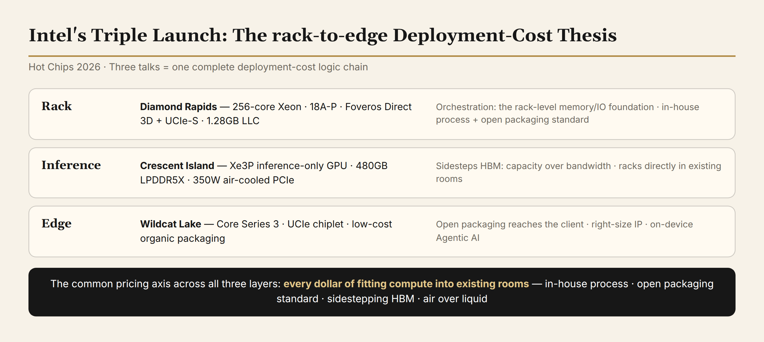
Intel delivered three talks at this conference: Diamond Rapids for the rack, Crescent Island for inference, Wildcat Lake for the edge, a narrative the company calls rack-to-edge. Individually, product launches; together, one complete deployment-cost logic chain: fab your own process, open your packaging standard, sidestep HBM on the inference card; every link compresses the cost of fitting compute into existing rooms. We call it the deployment-cost thesis, testing it link by link: where it holds, where it stalls.
1. Diamond Rapids: Packaging Engineering for the Rack Orchestration Layer
The engineering center of this rack-class Xeon is packaging. Foveros Direct 3D pushes die-to-die interconnect into direct bonding: bumps give way to sub-micron bonding pads, and die-to-die bandwidth per unit area rises by an order of magnitude. Diamond Rapids uses it for physical partitioning: compute dies and cache/IO dies are manufactured on their respective processes, then vertically composed into a 256-core processor with 1.28GB of LLC.
UCIe-S is the heavier step. Within the UCIe standard family, it is the specification layer for high-density interconnect inside advanced packaging, and it has mostly advanced alongside the accelerator-chiplet ecosystem; entering the Xeon mainline means Intel is shifting its primary CPU's die-to-die interface from proprietary protocol to open standard. Two consequences: third-party chiplets theoretically gain an interface path into Intel's main CPU package (vision level), and Intel's own combination becomes advanced-packaging-process-proprietary with an open interconnect protocol, corroborated by the client-side landing in §3.
The control-plane enhancements serve rack orchestration. APX doubles the general-purpose register count for instruction throughput on high-core-density servers; AMX enhancements let tensor computation complete on the CPU. The 256 cores, large LLC, and 16 memory channels serve agent-runtime orchestration, batch processing and tokenization, and KV-cache scheduling front-end logic; workloads whose primary consumption is core count and memory capacity, and AMX eliminates the PCIe round-trip for their tensor portions.
18A-P in-house production is the thesis's precondition: officially ~30% higher low-voltage frequency (futurumgroup), already in volume production. Diamond's cost advantage rides entirely on 18A capacity and yield: the first gate between the deployment-cost thesis and an actual price list.
2. Crescent Island: The Area-and-Power Tradeoffs of an Inference Card
The core of the area economics is the depth of the XMX array. Deepened to sixteen layers, weights flow through the array beat by beat, reused at every stage: the deeper the array, the more multiply-accumulates each byte of movement serves, and the lower the energy and area per unit of compute. The cost also grows with depth: fill-and-drain cycles take a larger share, and efficiency collapses at insufficient batch sizes. The number sixteen is itself a statement about workload assumptions: high-batch, regular autoregressive decode streams. Only a GPU whose sole purpose is inference can afford an array this deep.
Feature deletion points the same way. All 3D graphics and ray-tracing hardware is removed, and the freed transistors are reinvested in XMX density and LPDDR5X capacity (32MB unified L2, single source; branded cards 160GB, ODM up to 480GB), with numeric formats spanning FP4/MXFP4 through FP64. The trade holds only if the inference market no longer requires this chip to perform graphics functions.
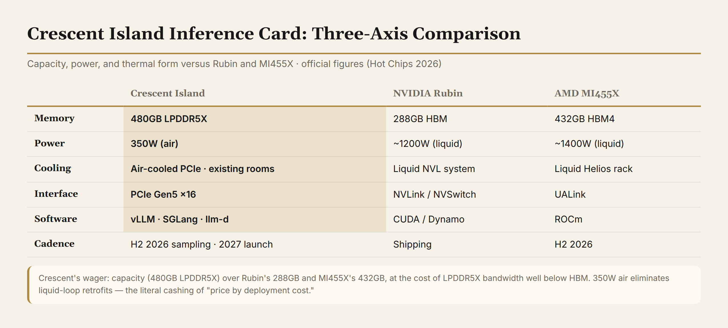
The memory medium is this card's entire wager. HBM supply is tight and prices are rising (the memory-wall piece has the detailed analysis); Crescent sidesteps with LPDDR5X. On-paper capacity of 480GB exceeds Rubin's 288GB and MI455X's 432GB (fig2); the cost is LPDDR5X bandwidth significantly below HBM. The stated design goals point explicitly at tokens per watt and agentic workloads. Agentic loads have large KV footprints and expensive recomputation: capacity buys throughput here, and the decode-side bandwidth shortfall is covered in software by KV-cache-aware routing and prefill optimization.
The deployment side is the plainest of the changes, and the most literal cashing of "price by deployment cost." 350W air-cooled PCIe Gen5 x16 mounts directly in standard racks with zero liquid-loop retrofit; vLLM, SGLang, and llm-d support arrives native, plus the NVIDIA Dynamo path, with the engineering cost of integrating into existing inference stacks priced together with the card. The counter-example sat on the same stage: MAIA 200's TDP provision reads 750W (hyperscaler piece), leaving power and thermal pressure to the system layer; Crescent keeps both within what a card can bear, and the two routes part ways on the power figure.
As a cross-reference to the hyperscaler piece: Google shapes silicon for workload (the 8i stacks bandwidth and SRAM); Intel shapes silicon for memory economics (LPDDR5X stacks capacity). The two routes diverge on whether decode lacks bandwidth or capacity, and the answer most likely varies by workload.
3. Wildcat Lake: Open Packaging Reaches the Client
Wildcat Lake is a client SoC, and the point of interest is the substrate: low-cost organic packaging, no Foveros-class stacking, die-to-die over UCIe chiplet. UCIe's applicability widens accordingly: open chiplet interconnect delivers high bandwidth inside advanced packaging (§1's UCIe-S) and serves cost-sensitive designs on low-cost traditional substrates. A standard covering both ends of the packaging-cost spectrum gives a third-party chiplet ecosystem its physical basis.
The first landing is a client SoC for a reason of volume: client shipments are the fastest at-scale validation an open standard can get. Right-size IP (ServeTheHome's on-site framing) embodies the same logic: tailor IP scale to the workload, connect back via standard interconnect, at lower cost than redesigning an entire single die. On the workload side, the local-small-model-plus-cloud-large-model routing of on-device Agentic AI is acutely cost-sensitive and fits exactly such a chip. Core configuration 2P+4E, NPU 17 TOPS (single-source transcription).
UCIe thus spans datacenter and client at once, taking Intel's differentiation weapon beyond pilot-project scale.
4. The CPU Ensemble: AGI, Vera, MONAKA
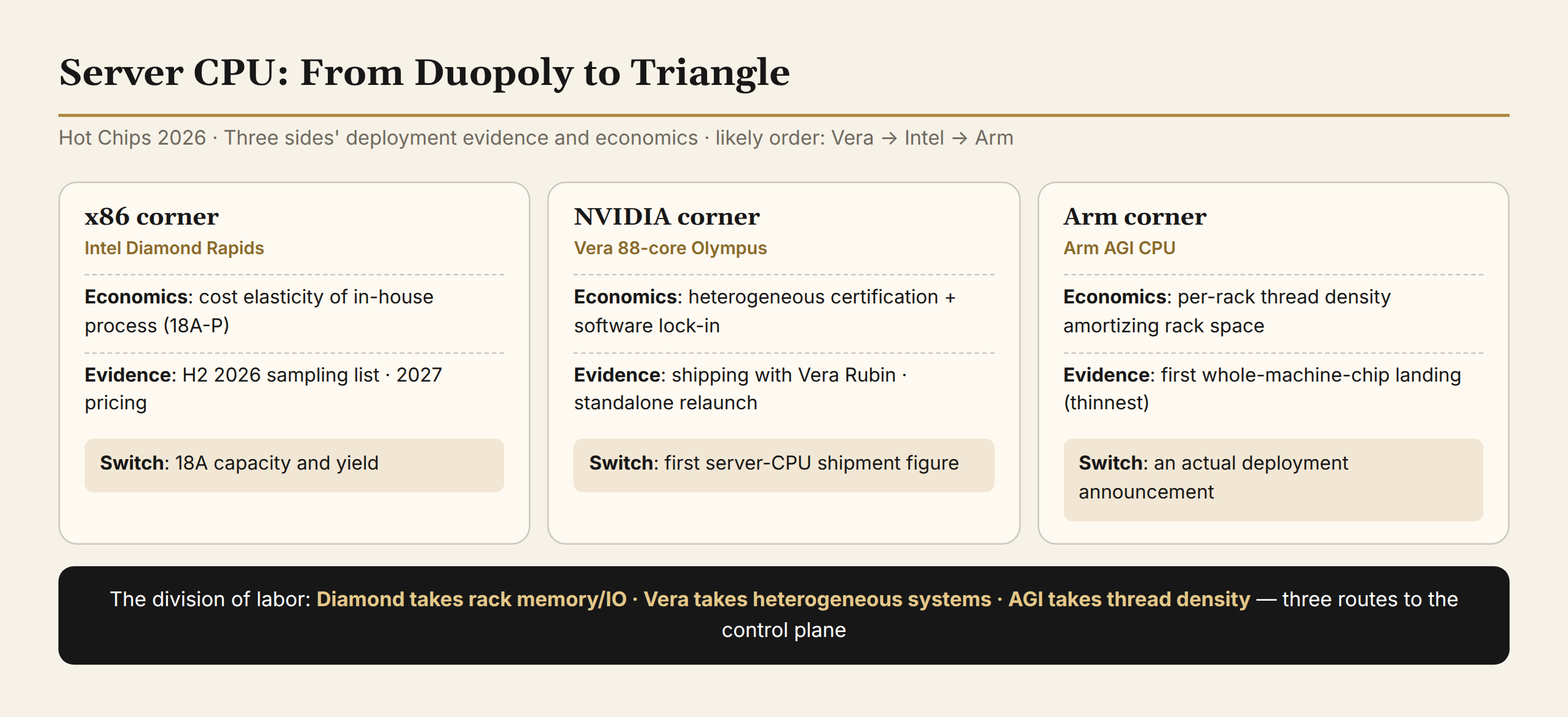
Arm AGI rewards analysis most for its yield design: 140 cores in hardware, 4 reserved for die harvesting, 136 delivered; TSMC 3nm dual chiplets spread the yield risk of a large monolithic die, and redundant cores absorb cutting losses. The approach comes from GPUs and mobile SoCs, appearing on a general-purpose server CPU for the first time. Aggregate memory throughput exceeds 800GB/s, about 6GB/s per core (6×136≈816, consistent with the aggregate figure), with "usable threads per rack" among the official selling points. TDP 300W; the official rack reference is 8,160 cores (36kW rack, in 1U dual-node and 2U dual-socket chassis).
Vera's increment is timing only: in full production with Vera Rubin systems, the CPU standalone relaunch (GTC Taipei 5/31 context) makes NVIDIA a systems company that also sells CPUs — precisely the thesis of cpu-comes-back. MONAKA leads with green AI datacenter and presented no new information beyond its published specs.
One conceptual boundary needs stating: the Intel side's "orchestration layer" means the control plane, where agent runtime and workload scheduling land on the CPU; data-plane and IO orchestration (the network piece's BlueField "factory OS") is a separate line. NVIDIA's own decomposition of agentic workloads supplies first-hand confirmation: prompt and orchestration on the CPU, memory spanning CPU, DPU, CUDA, LLM, and network, security on CPU and DPU. The two lines meet at the rack and each holds its side.
5. RISC-V Sidebar
The tutorial day ran four RISC-V talks, and three developments are worth recording: the first public demonstration of CUDA on RISC-V, with NVIDIA extending its own software stack's boundary onto an open instruction set; the RVA23 profile converging scalar-extension fragmentation; and NVLink Fusion already counting ≥3 third-party processors in the lab. Relative to the two established routes of x86 and Arm, the open ecosystem's third path acquired its first engineering coordinates at this conference.
6. Summary and Judgments
Three launches plus one ensemble add up to a deployment-cost roadmap: process, packaging, memory medium, thermal form. Intel recombined the cost structure of every layer.
Judgment one: deployment cost is the common pricing axis of all three products. 350W air cooling eliminates liquid-loop retrofits; LPDDR5X sidesteps HBM inflation; UCIe openness lowers chiplet-interconnect ecosystem cost; 18A in-house locks in process cost. Four moves aimed at the same variable, the unit cost of fitting compute into existing rooms. All three talks put their official design goals in tokens per watt; the objective function has changed, and the compute arms race's old scoring is invalid.
Judgment two: UCIe open packaging is Intel's most distinctive differentiation weapon. Process layer (Foveros Direct 3D) stays proprietary while the interconnect layer (UCIe/UCIe-S) opens: the combination guards the manufacturing profit layer while pulling the ecosystem onto an interface standard Intel helps define. The Xeon mainline and the client first-landing are the two supporting ends; whether third-party chiplets appear is the verification condition.
Judgment three: server CPUs move from an x86 duopoly to a triangle, and each side has its own verification conditions. For x86, the cost elasticity comes from the in-house process, the evidence is the 2026H2 sampling customer list and 2027 pricing, and 18A capacity and yield are the gate. For NVIDIA, the evidence is the strongest — already in full production with Vera Rubin — with heterogeneous-system certification and software-stack lock-in as its competitive core, and the first server-CPU shipment figure after the standalone relaunch as the watch item. For Arm, the evidence is thinnest — first whole-machine-chip landing — with the opportunity in per-rack thread density amortizing rack space, and an actual deployment announcement as the first verification node. The most likely verification order: Vera (shipping) → Intel (2027 pricing) → Arm (deployment announcements).
What to watch: third-party tokens-per-watt measurements after Crescent's H2 2026 sampling; 2027 launch pricing; Intel's quarterly 18A capacity/yield disclosures; whether third-party UCIe chiplets appear after Wildcat's launch; AGI deployment announcements and Vera standalone shipment figures.
Forward commitment: Crescent's sampling measurements and 2027 pricing; we will come back to verify.
Data as of 2026-08-29. Technical parameters from Intel press materials, Hot Chips 2026 on-site coverage, and vendor presentation materials (ServeTheHome and others); single-source and transcribed figures are marked in the text.
Further reading: Hot Chips 2026 Overview · Four Routes Against the Memory Wall · Hyperscaler Silicon, Generation Two · Five Networks for the AI Factory · When the CPU Supercycle Meets Agents