
2026-08-27 · Hot Chips 2026 specialist piece · The Memory Wall
Three months ago, the SubQ audit piece closed with a line: SSA is the cheapest of the four routes against the memory wall; the other three sit in silicon, co-design, and system layers, mostly landing in 2027; that is the next piece's business. This is that piece.
Hot Chips 2026 put the whole wall on stage. The tutorial morning ran six memory talks back to back: industry analyst Jim Handy on the memory market, then Micron, Samsung, and SK hynix, all three memory makers on stage, with startups d-Matrix and Oxmiq supplying the radical samples; the RISC-V block followed in the afternoon. Day 2's morning added two more on moving compute into memory. The agenda density is itself the signal: this conference restocked the two heaviest routes of the four, the silicon side and the co-design layer.
This piece dissects those two in depth; every number is checked against official materials and multiple first-hand reports, and single-source figures are flagged inline.
1. How Thick Is the Wall: Micron's Four Bills
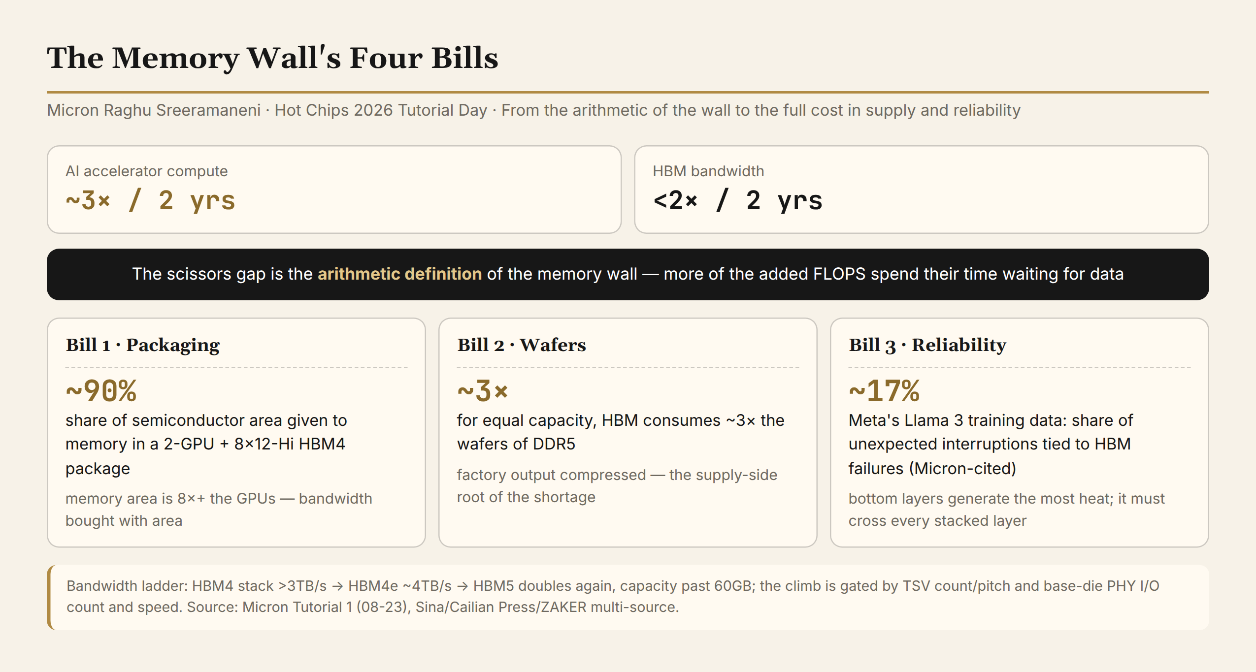
The scissors gap is the wall's arithmetic definition: AI accelerator compute roughly triples every two years; HBM bandwidth grows by less than 2×. The material Micron Fellow Raghu Sreeramaneni brought to the tutorial organizes the full cost behind the scissors into four bills.
Bill one, packaging. The latest-generation package integrates two GPUs with eight 12-high HBM4 stacks, and about 90% of the semiconductor area goes to memory, more than eight times the compute area. Bandwidth bought with area: the most immediately visible cost of the HBM route.
Bill two, wafers. For the same capacity, HBM consumes roughly three times the wafers of ordinary DDR5. The same fab sees its output compressed: the supply-side root of the persistent shortage. The tutorial's opening analyst, Jim Handy, arrives at the same number from the supply side: HBM yields only a third of the GB per wafer that standard DDR does, the industry has gone more than a decade without building major new fabs, and even an aggressive timetable needs about two years for new capacity (paraphrased). And the gap keeps widening: faster speeds, larger dies, more layers all demand more wafer area.
Bill three, reliability. Micron cited Meta's published Llama 3 training data: about 17% of unexpected training interruptions were tied to HBM failures. In a multi-layer stack, the bottom layers generate the most heat, yet the heat must cross every stacked layer to reach cooling at the top. Micron's read: the industry has entered the stage of measuring thermals first, then architecting the chip.
Bill four, the road ahead. HBM4 per-stack bandwidth already exceeds 3TB/s, HBM4e pushes toward the ~4TB/s range, and HBM5 doubles again relative to HBM4 with capacity past 60GB. But the bottleneck of the climb is explicit: TSV count and pitch, plus the I/O count and speed of the PHY in the base die. Stack height itself is not a free variable.
The four bills point to one conclusion, in Micron's own words: breaking the boundary between compute and memory through new architecture design will be one path over the wall. This conference's entire memory agenda is the delivery on that sentence.
2. Route One: Samsung Stacks Upward, Turning HBM into an SoC
Samsung's assault begins at the least glamorous spot: the base die.
In traditional HBM, the bottom die only forwards data and runs test functions, hosting the PHY that talks to the XPU. Samsung named two worsening problems: bandwidth doubles every generation, so TSV density and PHY power and area inside the base die have become the short pole; and the process gap between the base die and the XPU keeps widening, dragging integration efficiency down.
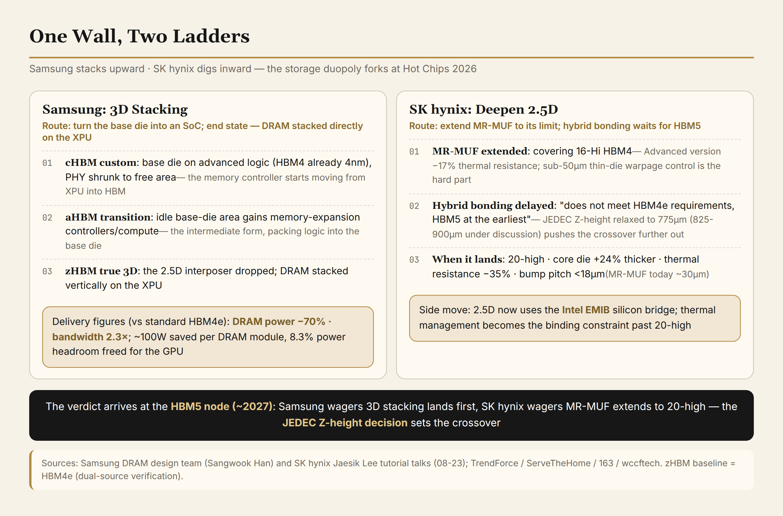
The counter comes in four moves. First, the base die moves to advanced logic: HBM4's base die is already on 4nm, materially narrowing the process gap with the compute chip. Second, custom HBM (cHBM): replace the traditional PHY with a die-to-die interface (shorter channels, smaller footprint) and hand the freed silicon back to the accelerator; per Samsung's account, sinking the memory controller into the base die frees 5% to 10% of XPU area, corresponding to ten-to-twenty-percent performance gains (paraphrased; performance figure single-source). Third, advanced HBM (aHBM): put memory-expansion controllers and compute onto the base die's idle area; the memory controller starts migrating from the XPU into the HBM. Fourth, the end state, zHBM: drop the 2.5D interposer and stack DRAM vertically, directly on the XPU, with ultra-high-density copper hybrid bonding delivering thousands of connections per square millimeter.
Thermals are the unavoidable companion of the custom phase: cHBM4 introduces the Heat Path Block, laying dedicated heat paths across roughly half of the PHY hot zone, pressing peak temperature down by more than 35% (paraphrased).
Delivery figures, baselined against standard HBM4e: DRAM power down 70%, bandwidth up 2.3×; each DRAM module saves roughly 100W and frees 8.3% of power headroom for the GPU.
The ambition of this route is not a memory spec but an identity: HBM evolving from memory package to memory-side SoC. Today's base die is a passive relay; Samsung wants it to take on scheduling and preprocessing functions. The backdrop is a market-share chase: in Q1 2026, SK hynix took 58% of the HBM market, with Samsung and Micron at 21% each (sell-side citation, flagged single-source). Samsung, tied with Micron in the second tier, cannot get there by running another lap on the same track; it needs a route that redefines the rules.
3. Route Two: SK hynix Digs Inward, Hybrid Bonding Waits Another Generation
In the same tutorial block, SK hynix answered with the opposite temperament: no architectural leap, extract the full potential of 2.5D.
Its MR-MUF process saw its lease extended to 16-high HBM4. Sixteen-high stacking is a demanding number: dies must thin below 50μm, warpage control becomes a manufacturing ordeal, and halving the inter-layer gap doubles the demands on underfill. Advanced MR-MUF cut thermal resistance another 17% versus the prior generation. What underwrites this choice is market position: more than half the HBM market is mortgaged to the yield of existing lines, and incremental improvement has the best risk-reward.
The real turn is the hybrid-bonding timetable. Copper-to-copper hybrid bonding is widely seen as the only road past 20-high, but SK hynix VP Jaesik Lee said it on stage, verbatim: it does not meet HBM4e requirements, HBM5 at the earliest. JEDEC's relaxation of package Z-height to 775μm, with 825-900μm under discussion, pushed the crossover point further out. The industry narrative of "hybrid bonding is imminent" meets, at SK hynix, a cool "one more generation."
The parameter sheet for when it finally lands is worth recording in full: 20-high stacking, core dies 24% thicker, thermal resistance about 35% below MR-MUF, bump pitch pressed from today's ~30μm to under 18μm. A further step: the 2.5D scheme explicitly adopts Intel's EMIB silicon-bridge interconnect; the wiring layer outside the stack is changing materials too.
There is a more fundamental line in this material worth lifting out on its own: HBM has gone from the last part mounted onto the system to the core that advanced packaging must design around from the start. CoWoS, EMIB, stack height, thermo-mechanical stress, power delivery, hybrid bonding, yield: the entire advanced-packaging line is being rearranged around HBM. Digging inward is, in substance, the memory maker taking the initiative back from the packaging houses.
Here the routes fork. Samsung bets 3D stacking lands first, trading generation gaps for architectural leaps; SK hynix bets MR-MUF stretches to 20-high, defending its base with yield and capacity. The verdict arrives at the HBM5 node, around 2027; JEDEC's Z-height decision sets the crossover point. One wall, two ladders: the industrial bet most worth tracking in this year's memory agenda.
4. A Startup's Proof: d-Matrix Raptor
The majors draw roadmaps; startups present evidence. d-Matrix's Raptor, presented in the tutorial block together with Meta, is a 3D-DRAM accelerator, and the most radical sample among the four routes.
The architecture can be stated in a single sentence: a TSMC N4 compute die, bonded face-to-face onto a custom DRAM chip at 36μm pitch. The orientation runs against intuition (logic on top, DRAM below) so the cold plate touches the compute silicon directly while the DRAM doubles as the interposer, with TSVs carrying PCIe and die-to-die signals.
The key numbers are about energy. CTO Sudeep Bhoja gave them on stage: the vertical interface costs about 0.37 pJ/bit, versus about 2.4 pJ/bit to move data into an HBM4 base die, a gap of more than 6×, and he stressed that every number comes from measurements on working silicon, with no paper extrapolation. The energy gap traces to the physical path: the vertical interface is a direct bond between dies, with data traveling distances measured in microns; entering HBM4 requires the long PHY path through the base die and a detour across the interposer. The conference-level ranges (2.5-5 pJ/bit for the 2.5D path versus 0.3-0.4 for vertical 3D I/O) agree. A single card carries 32GB at 100TB/s. An ISCA 2026 paper with the University of British Columbia projects roughly 4.7× higher throughput per card than an HBM-based design.
Raptor's most consequential part is its workload taxonomy, which ties the memory wall back to inference economics: prefill tends to be compute-bound, decode is bound by memory and bandwidth, and MoE can become capacity-bound at modest batch sizes. What truly needs extreme memory bandwidth is decode. This cross-confirms the overview's five-route picture, except Raptor compresses its answer into the package.
The commercial side is all projection-grade: the DRAM maker is undisclosed; there were no dates, volumes, or prices on site; the CEO said in June that the plan is 2027; the 2.8-trillion-parameter Kimi K3, 1M-token-context, 988 tokens/s per user figures are all early-silicon projections.
Its value is not a product timetable but a directional proof: AI inference innovation is shifting from adding multipliers to shortening data movement. That line, from the conference floor, can serve as the guiding thesis for the silicon side.
5. The Co-Design Layer: Compute Moves into Memory, from Research to Product
If the silicon side shortens the movement distance, the co-design layer changes what gets moved: let computation happen where the data resides. This conference delivered three landed paths.
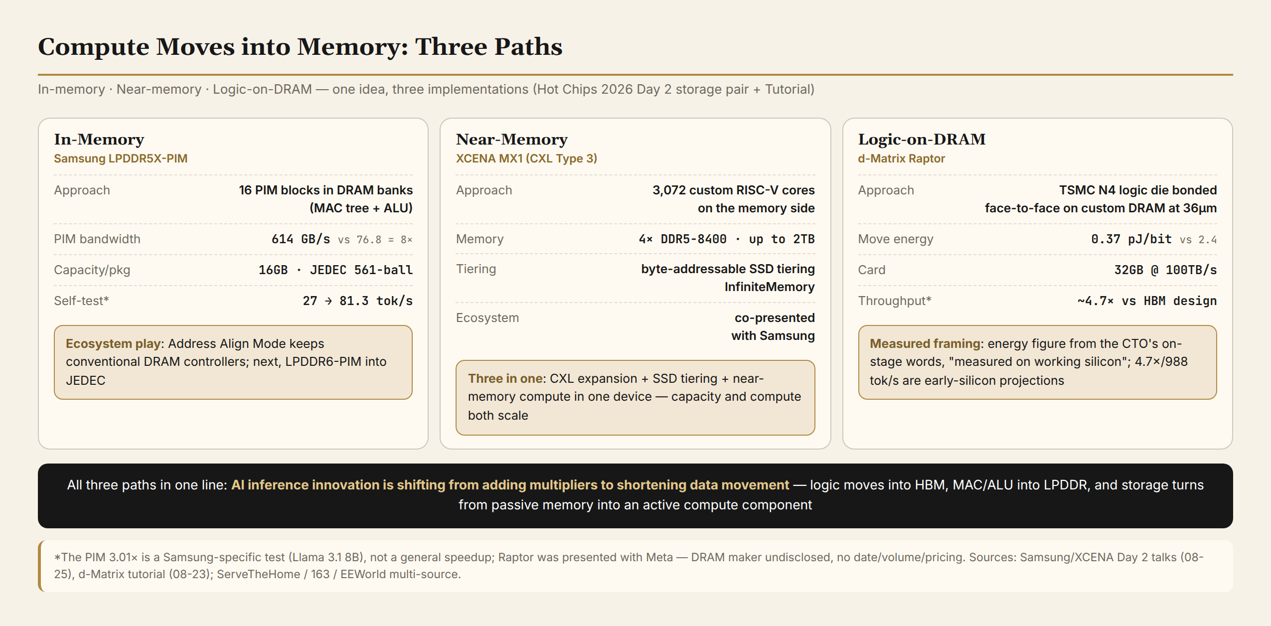
In-memory compute: Samsung LPDDR5X-PIM. Samsung placed 16 PIM blocks directly inside the DRAM banks, each integrating a MAC tree and an ALU, so part of the computation finishes inside memory instead of riding the bus into a processor. The energy spent moving a byte to the processor and back far exceeds the energy of computing on it where it sits — the physical motive behind PIM research. This is the first productized LPDDR-based PIM: 16GB, four dies per rank, in a standard JEDEC 561-ball package. The spec numbers: PIM internal bandwidth of 614GB/s, eight times the 76.8GB/s of the conventional LPDDR5X x64 side; about 2.4 TOPS at SINT4 weights.
Two design details matter more than bandwidth. First, Address Align Mode lets customers keep conventional DRAM controllers instead of redoing the memory subsystem. Compatibility is what carried PIM from a decade of papers to its first product. Second, Samsung's next step is taking LPDDR6-PIM into JEDEC standardization: only when a vendor feature becomes an industry standard does the route hold. The self-test number must be read with its framing: Llama 3.1 8B output rising from 27 to 81.3 tokens/s — that 3.01× gain comes from a Samsung-specific test, not a general speedup.
PIM is not a new concept. Samsung tried it on HBM2 back in 2021 with Aquabolt-XL; it took five years to reach LPDDR productization, and that five-year gap is itself a footnote: the distance from research to product is more than chip engineering.
Near-memory compute: XCENA MX1. The Korean startup co-presented MX1 with Samsung, and the chip is taped out on Samsung Foundry 4nm, so the joint session is more than an endorsement. Its approach puts 3,072 custom RISC-V cores next to the memory controller: 24 subsystems, each with four clusters totaling 128 processing units, each subsystem sharing a 128MB L3 cache. The cores are deliberately simple in-order cores, because the target workloads (in-memory analytics, RAG retrieval, memory compression) are bound by bandwidth and power, not single-thread performance; a vector engine adds a data-parallel path on top, roughly 3 TFLOPS of peak dot-product throughput per SoC.
On the CXL side, four DDR5-8400 channels expand up to 2TB; PCIe 6.0 also brings in SSDs, organized into a byte-addressable tiered capacity space via 64KB pages, an architecture XCENA calls InfiniteMemory, with DRAM caching SSD pages. The software stack provides a MapReduce-style runtime called PXL, kernels written in C/C++ or Rust, host and device sharing one virtual address space, so existing malloc-based code moves to CXL memory with minimal change.
Two sets of self-test results follow, in their original framing. Analytics kernels (Xeon 6767P reference, excluding idle power): throughput up to 4.7× the host-over-CXL path and 2× local DRAM, at roughly a quarter of host power. The KV cache experiment (Llama 3.1 8B with vLLM and LMCache): with a pinned prefix, first-token latency runs at 1.13× DRAM residency; removing the pin raises it to 1.57×, with a raw-SSD baseline at 1.86×, while lookahead prefetch narrows the gap back to near-DRAM levels. Samsung's companion move: open-sourcing its near-data-computing library, the NDC API, through OCP, with PyTorch reaching the PXL stack through OpenXLA, no framework code changes.
Another ecosystem signal from the session is worth recording: Samsung said CXL is being adopted by all the major cloud providers for databases and AI KV cache. The sentence describes the CXL ecosystem, not this particular device; but the ecosystem maturing ahead of the device is the precondition for this route's viability.
The third use of stacking. Put §4's Raptor back into this frame and the three paths are one logic in three implementations: logic moves into HBM (base-die SoC-ization), MACs and ALUs move into LPDDR (PIM), the compute die sits straight on DRAM (Raptor). Storage is turning from a passive repository into an active compute component; that observation from the conference floor is the common denominator of all three.
6. Algorithm and System Layers: Positioning and Handoffs
The other two routes of the four get one positioning paragraph each.
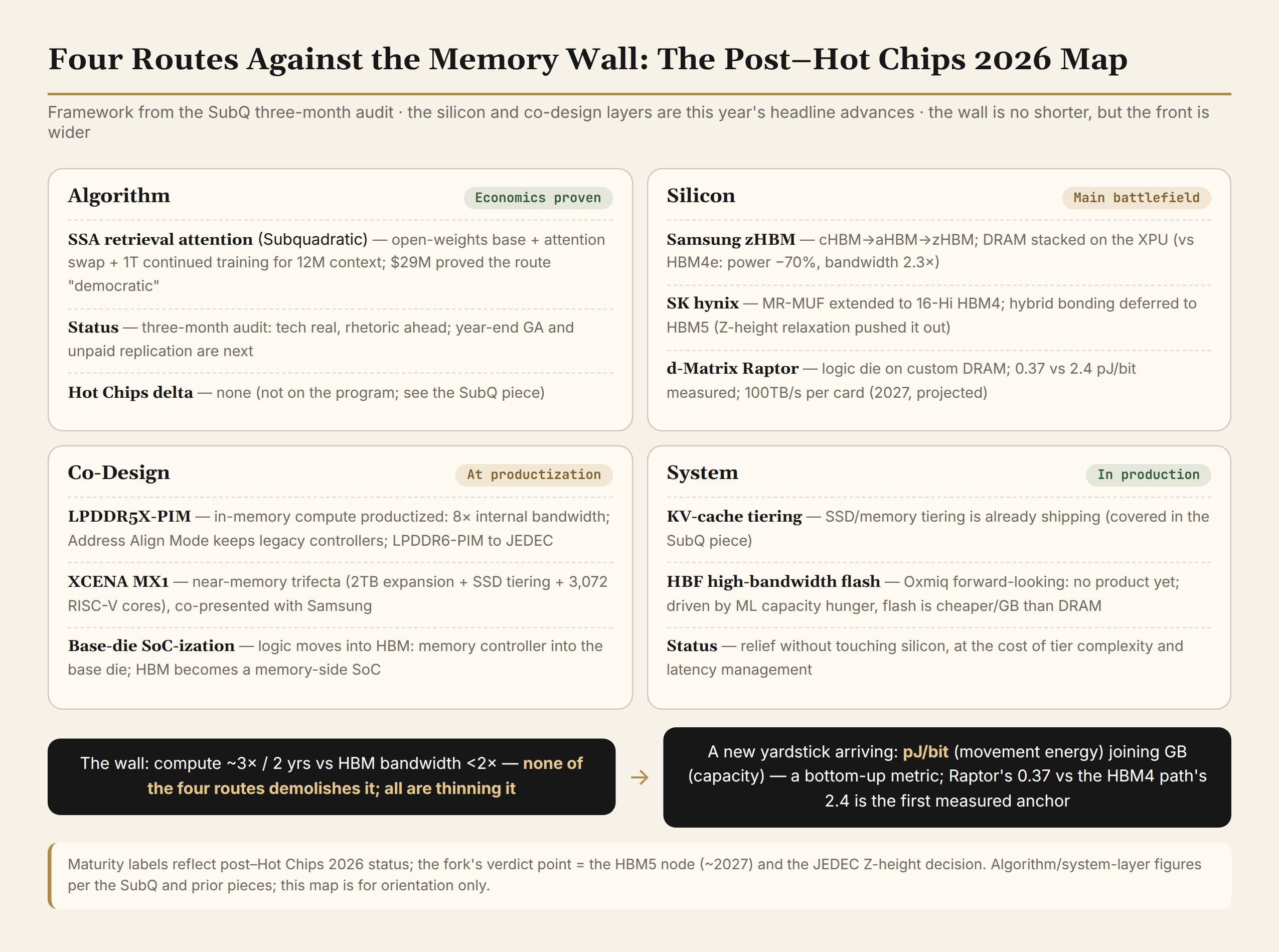
The algorithm layer is the cheapest route. Subquadratic used an open-weights base plus an attention swap plus 1T of continued training to reach 12M context for $29M, proving the algorithmic route is democratic: no frontier-lab budget required. The three-month audit's verdict still stands: the tech is real, the rhetoric ran ahead; year-end GA and unpaid third-party replication are the next checkpoints.
The system layer is in mature production. KV-cache tiering sinks cold data to SSD as a shipping route; this year's HBF high-bandwidth flash tutorial (Oxmiq) is the layer's long-range option: no product yet, purely forward-looking, resting on flash's order-of-magnitude cost advantage per GB over DRAM. The system layer relieves pressure without touching silicon, at the price of tier complexity and latency management.
Put the four routes on one map: the algorithm layer is democratized, the silicon side is forking, the co-design layer is crossing into product, the system layer is mature. The wall has not become lower, but the front has widened.
7. Judgments and What to Watch
Judgment one: the yardstick is moving from GB to pJ/bit — a re-standardization from the bottom up. The capacity race is over and the movement race has begun, a judgment the overview set down; here it advances to where it can be measured. In the capacity race, memory was measured in bandwidth and capacity; in the movement race, the measure is energy per bit moved. But the new yardstick's provenance must be stated precisely: it is currently pushed from below by startups and papers, and the three majors' datasheets still quote only TB/s and GB. Raptor's 0.37 versus 2.4 pJ/bit is the first measured anchor from working silicon; zHBM's 70% power reduction and MR-MUF's 35% thermal-resistance cut are variants of the same yardstick. The new measure is arriving, not yet rewriting. HBM5-era datasheets printing pJ/bit would be the signal that the shift is accelerating; two generations of silence from the three majors would send it back to an academic measure. Reading memory roadmaps from here on, look first for where the pJ/bit sits.
Judgment two: the packaging fork is the biggest variable of the next two years, settled where three things converge around 2027. Samsung's 3D stacking and SK hynix's deepening of 2.5D meet head-on at the HBM5 node. What "settled" means must be pinned: three things converging in the same window — the HBM5 node forcing the final hybrid-bonding decision; JEDEC's Z-height ruling setting the crossover point; and whether zHBM can hand over silicon and a deployed workload. The market-share reversal forecasts (sell-side, single-source) stay in the background and carry no weight. We read this as more than a technical bet: the chaser needs a lane change; the leader needs the compounding of existing lines. The test window is 2027 itself: if zHBM is still a slide by then, the fork degrades to posture; if hybrid bonding gets pulled back into the HBM4e node, the fork's premise inverts.
Judgment three: near-memory compute has crossed the productization threshold, but scale commercialization is still two gates away — cost and ecosystem. The evidence line, stated in its original framing: PIM has a JEDEC standardization track and its first LPDDR product; MX1 has a card demonstrated running and a reproducible vendor benchmark suite. Samsung added an ecosystem-leading signal on stage: CXL is being adopted by the major cloud providers for databases and AI KV cache. All remain niche: PIM's gains are workload-specific (the Samsung self-test framing is mandatory), software stacks must be rewritten for in-memory compute, and MX1's CXL ecosystem is still climbing. Past those two gates, a second inference-memory market appears beyond HBM. The leading indicator for the ecosystem gate: whether a second DRAM maker joins PIM. If LPDDR6-PIM never reaches JEDEC and no second maker ever follows, the threshold claim needs recomputing.
Six checkpoints: the JEDEC Z-height ruling; LPDDR6-PIM standardization progress; whether a second DRAM maker joins PIM (the ecosystem gate's leading indicator); d-Matrix's 2027 delivery; zHBM's first deployed workload; and Micron's HBM5 roadmap (this year it drew the wall and offered no ladder; next year it must deliver its own answer). When the JEDEC ruling and the three makers' 2027 roadmap updates land, this series will come back to verify.
Data as of 2026-08-29. Technical parameters from Hot Chips 2026 vendor presentation materials, official releases, and on-site reporting (ServeTheHome among others); self-reported, paraphrased, and single-source figures are flagged inline.
Further reading: The SubQ Three-Month Audit (the algorithm layer and the four-route framework) · Hot Chips 2026 Overview (the direction map and its judgments) · When SSD Becomes Memory (the system layer's KV tiering) · The Tyranny of VRAM (the KV-cache full-stack view)