
In March 2026, Jensen Huang published a rare long-form essay titled "AI Is a 5-Layer Cake." AI is not a single application or model, he argued, but a new type of infrastructure—like electricity and the internet. He divided the AI industry into five layers: energy, chips, infrastructure, models, and applications, stacked bottom to top, each supporting the one above.
The layer most easily overlooked is energy, at the very bottom. Huang's words: "Energy is the physical foundation of intelligence generation, and the ultimate ceiling of industry scale." No matter how good your chips or how clever your models, if electricity can't be delivered reliably, stably, and affordably, everything above collapses to zero.
Bank of America Securities clearly understood this. Two months later they published a report that didn't quite read like a typical semiconductor research note—titled "Watts to Tokens," it converted every kilowatt-hour of electricity into AI-generated tokens, positioning power semiconductors as the "shovel sellers" of the new era.
Rack Power Consumption Has Surged 100x, Pushing Power Distribution Architectures Into a Corner
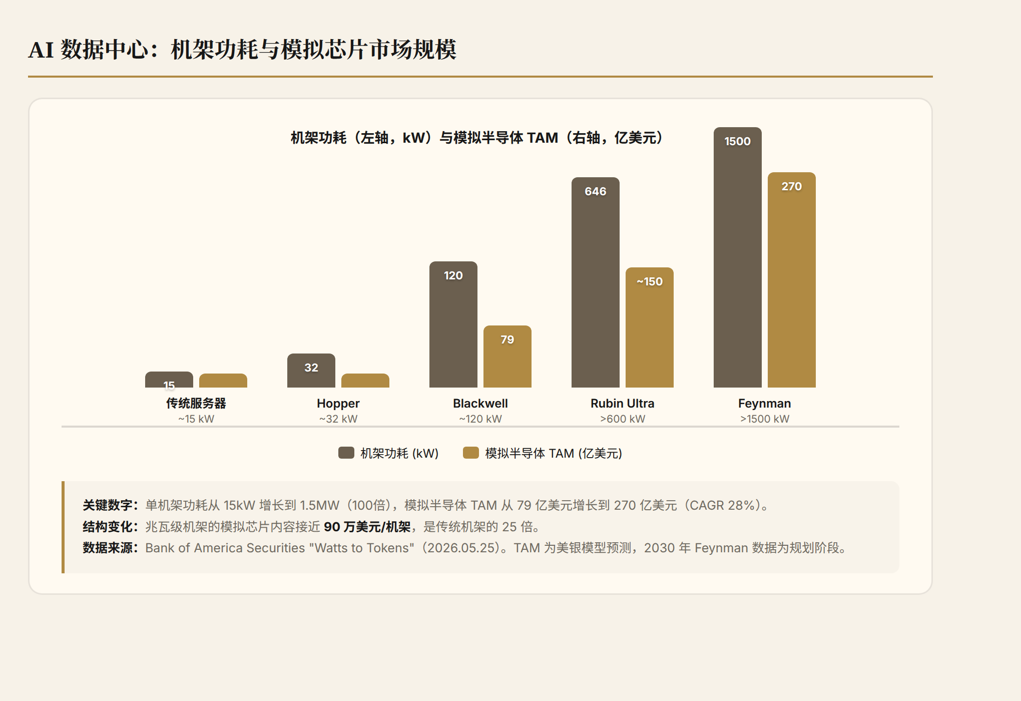
On May 25, 2026, Bank of America Securities published the report. The core numbers are striking:
| GPU Platform | Single Rack Power Consumption | Period |
|---|---|---|
| Traditional Server | 10-15 kW | 2023 |
| Hopper (H100) | ~32 kW | 2024 |
| Blackwell (B200) | ~120 kW | 2025 |
| Rubin Ultra | >600 kW | 2026-2027 |
| Feynman | >1,500 kW (1.5 MW) | 2029-2030 |
Within a decade, rack power consumption has surged nearly 100-fold. But can power distribution providers keep up with this growth rate?
They can't. The existing 54V DC power distribution architecture has already hit a physical ceiling. If a megawatt-class rack still uses a 54V power supply, the power system would occupy 64U of rack space—leaving the entire cabinet for power, with no room for the GPUs. The weight of copper busbars, the cross-sectional area of cables, and the thermal losses from multi-stage AC/DC conversion all point to the same conclusion: the physical headroom on this path has been completely exhausted.
800V DC Power Distribution: Not an Optional Upgrade, but an Inevitability Forced by the Laws of Physics
NVIDIA released a white paper at the October 2025 OCP Summit: 800VDC Architecture for AI Infrastructure. Not a concept demo, but a production roadmap.
Core concept: compress the traditional 4-5 stages of power conversion into 1-2 stages.
Traditional power distribution chain (415V AC system):
13.8kV Medium Voltage AC → Low Voltage Switchgear → UPS → PDU → PSU(AC/DC) → Board-level DC-DC → GPU
      ↓                           ↓                  ↓       ↓        ↓                  ↓
    Efficiency loss            Efficiency loss   Efficiency loss Efficiency loss Efficiency loss Efficiency loss
Every conversion stage incurs losses; at the 54V endpoint, the current is massive—P=I²R, meaning resistive losses scale with the square of the current.
800V DC power distribution chain:
13.8kV Medium Voltage AC → SST/Centralized Rectification → 800V DC Bus → Rack-level DC-DC → GPU
      ↓                           ↓                          ↓                  ↓
    Single-stage conversion     1-2 stages                Low-current transmission Final regulation
The key benefit isn't "a few percentage points of efficiency gain," but structural simplification:
- Transmitting the same power at 800V drops the current to roughly 1/15 of that at 54V, and resistive losses plummet to approximately 1/225
- Under a 1GW IT load, facility-level power consumption drops by roughly 5%, equivalent to continuously saving 69MW—slashing tens of millions of dollars off the annual electricity bill
- A DC bus is just two conductors, eliminating AC switchgear, low-voltage AC PDUs, and in-rack AC/DC power supplies
- Energy storage systems (supercapacitors + batteries) connect directly to the DC bus, smoothing out the millisecond-scale 30%-100% load fluctuations inherent in AI training, and eliminating the AC→DC→AC double conversion of traditional UPS
NVIDIA's evolution roadmap is clear:
| Phase | Solution | Efficiency | Status |
|---|---|---|---|
| Current Mainstream | Traditional UPS (3-4 stages conversion) | ~92% | Still in use but hitting limits |
| Transition Period | 240V/380V HVDC | ~95-97.5% | Currently rolling out |
| 2026-2027 | 800V HVDC (Sidecar cabinet solution) | ~97% | Advancing in sync with Kyber racks |
| 2028+ | SST (Solid State Transformer, Medium Voltage AC directly to 800V DC, 1 stage) | ~98.5% | Demo → Scale-up |
NVIDIA made it clear: starting in 2027, 800V HVDC will enter full production in sync with the Kyber rack-level system. The partner ecosystem includes nearly 30 companies such as Infineon, TI, Delta Electronics, Flex Power, Megmeet, Vertiv, and Schneider. It's not an exclusive lock-in, but the barrier to entry for the approved vendor list is high.
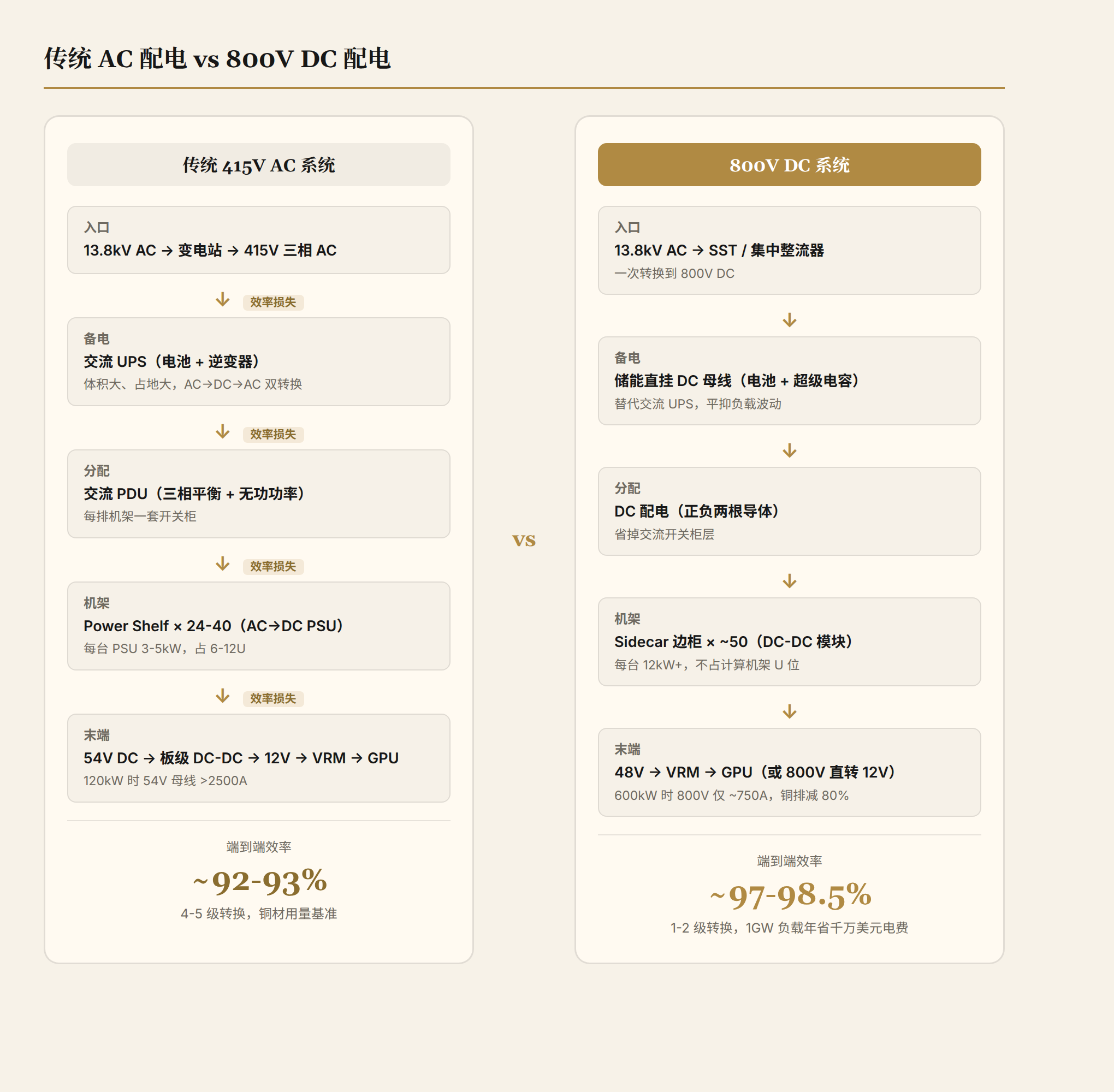
Device-Side Stage-by-Stage Breakdown: What Happens at Every Level from the Grid to the GPU Core
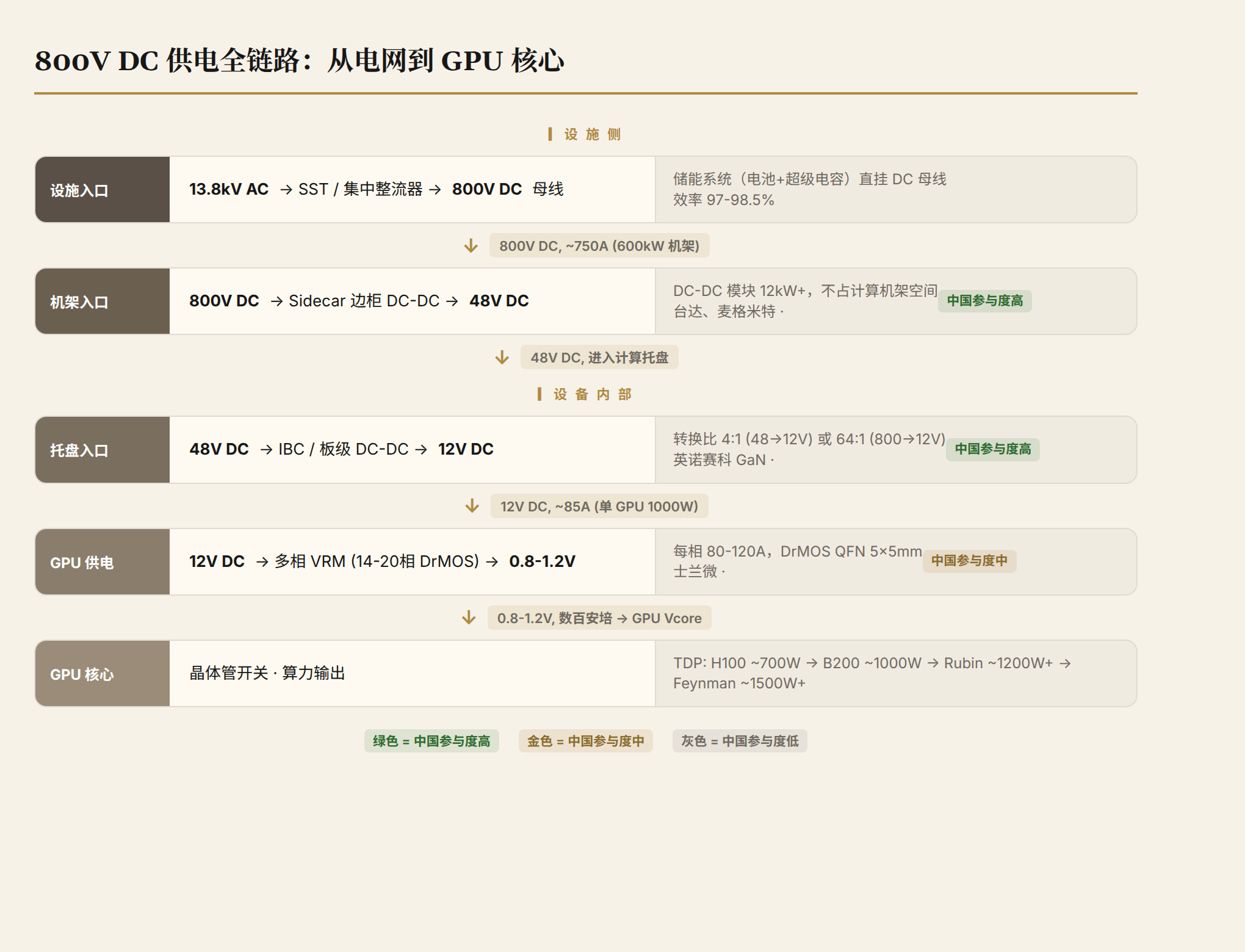
The previous comparison was at the facility level, from the grid to the rack inlet. However, the 800V transition isn't just about the data center room; it changes the power architecture inside servers and switches. This section breaks down every stage of the power delivery chain, examining the physical form factor, key components, and retrofit requirements of the equipment under both the old and new paradigms level by level.
Stage One: Facility Inlet — Medium Voltage AC to Data Center Power Distribution
Old Model (415V AC System):
13.8kV AC → Substation step-down → 415V 3-phase AC → AC UPS → AC PDU → Rack
- The substation steps down medium voltage to 415V 3-phase AC, passing through an AC UPS (battery + inverter) for backup power protection
- The AC PDU distributes power to each row of racks, requiring management of 3-phase balancing, reactive power, and ground fault detection
- Massive AC cables are laid within the data center, with one switchgear per row of racks
- Facility-level UPS efficiency is 92-95%; large footprint and volume
New Model (800V DC System):
13.8kV AC → SST/Centralized Rectifier → 800V DC Bus → DC Distribution → Rack
- SST (Solid State Transformer) or centralized rectifier converts 13.8kV AC to 800V DC in a single stage
- The DC bus has only positive and negative conductors, drastically simplifying cable trays
- Energy storage systems (batteries + supercapacitors) are directly connected to the DC bus, replacing traditional AC UPS
- Facility-level efficiency reaches 97-98.5%, eliminating the entire AC switchgear layer
Impact on Servers/Switches: The equipment in this stage is all on the facility side; servers do not participate directly. However, there is an indirect impact: under the old model, every server PSU needs to accept AC input and perform its own AC/DC conversion; under the new model, the PSU input becomes 800V DC, resulting in a completely different topology.
Stage Two: Rack Inlet — Power Shelf vs Sidecar
Old Model: Power Shelf
AI server racks (like GB200 NVL72) install a Power Shelf in the middle or on the side of the rack, which is a chassis that centrally houses PSU modules.
415V AC → Power Shelf (multiple PSUs in parallel) → 54V DC Copper Busbar → Compute Tray
- Each PSU accepts 415V AC input and outputs 54V DC
- Typical PSU power is 3-5kW; a 120kW rack requires 24-40 PSU modules
- 54V DC is distributed to compute trays via copper busbars
- At 120kW, the 54V bus current exceeds 2500A; the copper busbar cross-section is large and heat generation is severe
- The Power Shelf occupies 6-12U of rack space, squeezing the space for compute equipment
- Typical efficiency: AC/DC PSU ~94%, Power Shelf overall ~93%
- Standard: OCP Open Rack V3 specification defines the 48V/54V power shelf interface
New Model: Sidecar + 800V DC Direct Inlet
800V DC → Sidecar (Centralized DC-DC) → 48V/50V DC → Compute Tray
     or
800V DC → In-rack DC-DC Module → 12V DC → Compute Tray
The NVIDIA Kyber rack adopts the Sidecar approach—power modules are placed in an independent side cabinet, side-by-side with the compute rack:
- The Sidecar accepts 800V DC input, centrally converting it to 48V/50V DC (transitional solution) or 12V DC (ultimate solution)
- A 600kW rack at 800V draws only about 750A total current, reducing the busbar cross-sectional area to 1/15th of the original
- The Sidecar does not occupy U-space in the compute rack, unlocking compute density
- A single DC-DC module can reach 12kW+, requiring only about 50 modules to cover 600kW
- STMicroelectronics demonstrated a complete chain solution for 800V DC direct-to-12V and 6V at GTC 2026
- Typical efficiency: 800V→50V DC-DC ~97%, 800V→12V DC-DC ~96%
Key Difference: Old PSUs perform AC→DC conversion (415V AC→54V DC), while new modules perform DC→DC conversion (800V DC→48V/12V DC). The topology, components, and control logic are completely different. You cannot plug an 800V module into an old Power Shelf; the physical interface of the rack power distribution needs to be redesigned.
Stage Three: Compute Tray Inlet — Board-Level DC-DC
Old Model (54V→12V→GPU):
54V DC Copper Busbar → Tray Connector → Board-Level DC-DC (54V→12V) → 12V Distribution Plane → GPU
- The compute tray draws 54V from the copper busbar via an edge connector
- On-board DC-DC steps down 54V to 12V, typically using LLC resonant or Buck topologies
- 12V power is distributed to the GPU and CPU via PCB traces
- A single GPU (TDP 700-1000W) requires 60-85A of current at 12V; PCB copper thickness and trace width are hard constraints
- Components at this DC-DC stage: Silicon-based MOSFET + driver IC + inductors/capacitors, which is the traditional domain of analog/power semiconductors
New Model (800V Direct to Tray / 48V Transition):
Transitional solution:
48V/50V DC → Tray Connector → Board-Level DC-DC (48V→12V) → 12V Distribution → GPU
Ultimate solution (NVIDIA's direction):
800V DC → Tray Connector → Board-Level DC-DC (800V→12V, 64:1 conversion ratio) → 12V Distribution → GPU
800V direct-to-12V is the most technically challenging stage in the entire chain: a 64:1 conversion ratio and 12kW power per module, requiring 96%+ efficiency in an extremely compact space.
- Topology selection: Primarily LLC resonant, with SiC/GaN devices replacing silicon MOSFETs for high-side switches Embedded PCB must be used, burying magnetic components and power devices into the inner layers of the PCB, using vertical power delivery to reduce plane footprint. The value of embedded PCB is several times higher than traditional PCB; the market size for embedded PCBs just in the 800V→12V primary power supply sector exceeds 35 billion RMB.
If 800V goes directly into the tray, the 54V→12V stage on the motherboard disappears, replaced by an 800V→12V high-voltage DC-DC. PCB layout, insulation spacing (800V safety spacing is much larger than 54V), and thermal paths all need to be redesigned. This isn't solved by just changing a power module; the entire motherboard requires a relayout.
Stage Four: GPU Core Power Delivery — VRM / Multiphase Power
This stage is the last mile of GPU power delivery. It sees the least change between the old and new models because the input is around 12V and the output is the core voltage of 0.8-1.2V in both cases. However, the current scale is climbing drastically.
VRM (Voltage Regulator Module):
12V DC → Multiphase VRM (80-120A per phase) → 0.8-1.2V GPU Vcore
- GPU core voltage is about 0.8-1.2V, but current can reach hundreds or even over a thousand amps
- Multiphase parallel: 80-120A per phase, a 1000W TDP GPU may require 12-16 phases
- Core components per phase: DrMOS (a single-package chip integrating driver + high-side MOSFET + low-side MOSFET) + inductor
- DrMOS packages are primarily QFN (5×5mm or 6×6mm), pursuing extremely low parasitic inductance
- Controller ICs communicate with the GPU via PMBus or SVID interfaces to regulate voltage and phase count in real-time
Old vs. New Model Comparison: The VRM stage is almost identical between the old and new models—the input is always 12V. What truly changes is the scale of the VRM:
| GPU Generation | TDP | 12V Current | VRM Phases | DrMOS Count |
|---|---|---|---|---|
| H100 | ~700W | ~60A | 10-12 phases | 10-12 |
| B200 | ~1000W | ~85A | 14-16 phases | 14-16 |
| Rubin | ~1200W+ | ~100A | 16-20 phases | 16-20 |
| Feynman (Estimated) | ~1500W+ | ~125A+ | 20-24 phases | 20-24 |
Each GPU generation increases TDP by about 20%, driving continuous growth in VRM phases and DrMOS usage. This is the stage with the most certain incremental growth for analog chips; regardless of how the power distribution architecture changes, the VRM demand for GPU core power will only increase.
Stage Five: Protection and Monitoring — eFuse, Hot Swap, Current Sensing
This stage is often overlooked but is crucial in megawatt-class racks.
Old Model:
- Each compute tray inlet has an eFuse (electronic fuse) for hot-swap protection at 54V
- Current sensing uses shunt resistors or Hall effect sensors
- Overcurrent protection response time is in the millisecond range, which is sufficient
New Model:
- eFuse design difficulty increases sharply under 800V DC—breaking an 800V DC arc is much harder than breaking 54V, requiring SiC devices for solid-state circuit breakers
- Current sensing requires higher precision sensors (a small error at 800V = a large power deviation)
- Hot-swap control must respond at the sub-millisecond level; otherwise, arcing will damage the connectors
- Infineon has already launched a 48V eFuse series and hot-swap controller reference design tailored for 400V/800V power architectures
Stage Six: Switch Power Delivery
The power consumption of network switches in AI clusters is also surging.
Old paradigm: Switch PSUs accept AC input (internal AC→DC conversion) or use 48V/54V direct supply. Typical power consumption is 500W-2kW, with current around 10-40A at 54V, which is not a major issue.
New paradigm: High-port-count InfiniBand or Ethernet switches (e.g., NVIDIA Quantum-X 800G) are seeing power consumption evolve toward 3-5kW. In an 800V DC environment:
- Switches require new PSU modules to accept 800V DC input
- Internal switch space is more constrained (reserved for optical modules and ASICs), so power modules must be extremely miniaturized
- 800V→12V/5V DC-DC conversion must be squeezed into 1U or even half-U of space
SemiAnalysis estimates that 800V adoption for switches and network equipment will lag GPU servers by 1-2 years, as switch power consumption has not yet reached the physical limits of 54V. However, by 2028-2029, when 51.2T or even 102.4T switches exceed 10kW in power consumption, they will face the same transition pressure.
Apple-to-Apple Full-Link Comparison Summary Table
| Power Supply Stage | Old Paradigm (54V AC System) | New Paradigm (800V DC System) | Key Changes |
|---|---|---|---|
| Facility Entrance | 13.8kV AC → Substation → 415V AC → AC UPS → AC PDU | 13.8kV AC → SST/Rectifier → 800V DC Bus → DC Distribution | Eliminates AC UPS/PDU layer; energy storage hangs on DC bus |
| Rack Entrance | AC PDU → Power Shelf (24-40 AC/DC PSUs) → 54V Copper Busbar | 800V DC → Sidecar Cabinet (~50 DC-DC modules) → 48V/12V | PSUs change from AC/DC to DC/DC; no AC cables within the rack |
| Tray Entrance | 54V → Board-level DC-DC → 12V | 48V/800V → Board-level DC-DC → 12V | With direct 800V input, conversion ratio increases from 4.5:1 to 64:1 |
| GPU VRM | 12V → Multi-phase VRM → 0.8-1.2V | 12V → Multi-phase VRM → 0.8-1.2V | Input unchanged, but phase count increases with TDP |
| Protection/Monitoring | 54V eFuse + Shunt Resistor | 800V SiC Solid-State Circuit Breaker + High-Precision Sensor | Voltage increases 15x; protection devices require re-selection |
| Switch PSU | AC Input or 54V Direct Supply | 800V DC Input (2028+) | Switch power consumption is still low; transition lags by 1-2 years |
| Typical Efficiency | 92-93% (End-to-End) | 97-98.5% (End-to-End) | Every 1% saved at GW scale = tens of millions of dollars in annual electricity savings |
| Copper Usage | Baseline | Reduced by ~80% | Current drops 15x; wire gauge shrinks proportionally |
| Rack Space | Power Shelf occupies 6-12U | Sidecar separated from compute rack | Compute density unlocked; more space for GPUs |
Practical Challenges of Retrofitting
After reviewing the stage-by-stage comparison, a natural question arises: can existing servers and switches be retrofitted and upgraded to 800V?
The answer is: almost impossible. The reason lies not in any single component, but in the fact that the interface definitions for the entire link have changed:
- PSU module incompatibility: Old PSUs accept AC input, while new modules accept 800V DC input. Socket shapes, pin definitions, and safety clearances are completely different
- Copper busbars must be replaced: The insulation class, cross-sectional area, and connector specifications of 54V copper busbars are unsuitable for 800V. Safety clearances increase from a few millimeters to tens of millimeters
- Motherboards must be redesigned: With 800V directly entering the tray, PCB insulation clearances, thermal paths, and DC-DC layouts must be completely redesigned from scratch
- Protection circuits must be rebuilt: 54V eFuses will break down at 800V, requiring SiC devices to build new solid-state circuit breakers
- Monitoring software must be adapted: The fault characteristics (arcing, short-circuit behavior) of DC distribution are completely different from AC; DCIM systems require updates
Therefore, the realistic path forward is: new datacenters will be built from the ground up with 800V, while older datacenters will continue using 54V until decommissioned. There is no smooth transition; these are two generations of incompatible power distribution architectures. NVIDIA's approach corroborates this: the Kyber rack is an entirely new design, not a retrofit of any existing rack.
Another Path Beyond 800V: Three Generations of Evolution in In-Device Power Delivery
So far, the discussion has focused on the facility side—the transformation of the power distribution architecture from the grid to the rack entrance. However, there is a parallel evolution line for in-device power delivery. It is not a replacement for 800V but rather advances concurrently: 800V solves "how to deliver power to the rack," while in-device power delivery solves "how to deliver power to the chip core." The two paths ultimately converge.
Generation 1: 12V Intermediate Bus Architecture (Traditional Servers)
The power delivery path for the vast majority of traditional servers:
PSU (AC→12V DC) → 12V Intermediate Bus → PCB Power Plane → VRM → CPU/GPU (0.8-1.2V)
The 12V bus architecture has dominated data centers for over two decades. Its advantage is simplicity—a single voltage plane distributes power to all components. But when single GPU power consumption exceeds 300W, the physical bottlenecks of 12V are exposed:
- A 700W H100 at 12V requires about 60A of current; the I²R losses transmitted through PCB traces are significant
- There is an upper limit to the current-carrying capacity of GPU slots and PCB copper layers
- The VRM (12V→0.8V) conversion ratio is 15:1, with an extremely low duty cycle (about 5-7%), leaving limited room for efficiency optimization
The 12V architecture is sufficient for traditional CPU servers (TDP 200-350W), but it has reached its limits in the era of AI accelerators.
Generation 2: 48V Direct (Scaling Up)
Google was the earliest to push 48V into servers. In 2017, Google released the Zaius POWER9 server, delivering 48V directly to the motherboard and bypassing the 12V intermediate bus. Since then, the OCP (Open Compute Project) has incorporated 48V into the Open Rack V3 specification, making it the evolutionary direction for industry standards.
Key Changes in the 48V Architecture:
PSU (AC→48V DC) or 800V DC → DC-DC → 48V Bus → IBC (48V→12V) → VRM → GPU
                                                        or
                                                   48V Direct to VRM → GPU (0.8-1.2V)
The benefits of 48V over 12V are mathematical: transmitting the same power, the current drops to 1/4, and I²R losses drop to 1/16. For AI servers with single GPU power consumption of 700W+, this means:
- Significant reduction in thermal stress on PCB traces and connectors
- Relaxed copper layer thickness requirements, freeing up more PCB layers for signal routing
- Thinner cables and smaller connectors can be used
Once 48V enters the device, there are two paths:
Path A: 48V→IBC→12V→VRM→GPU (Two-step conversion, transitional solution)
The IBC (Intermediate Bus Converter) steps down 48V to 12V, and then a traditional VRM steps down 12V to the core voltage. The advantage is that the VRM doesn't need to be changed, maintaining compatibility with existing designs. The disadvantage is an extra conversion stage, resulting in an efficiency loss of about 2-3%.
Path B: 48V Direct to VRM→GPU (One-step, ultimate direction)
48V is fed directly into the VRM, which steps it down directly to the 0.8-1.2V core voltage. Eliminating the IBC stage yields higher efficiency. However, the challenges are significant:
- The conversion ratio is 48:1 (48V to 1V), with a duty cycle of about 2%. Traditional Buck topologies suffer from poor efficiency and transient response at this duty cycle
- Switched Tank or LLC resonant topologies must be used, combined with coupled inductor technology to extend the effective duty cycle
- Companies like Vicor, MPS, and Infineon have introduced 48V direct-to-core voltage solutions with power densities exceeding 1000W/in³
Currently, mainstream AI servers (like GB200) adopt Path A—48V enters the rack, IBC converts it to 12V, and VRM then converts it to the core voltage. Path B is the next step, requiring further maturation of VRM components and PCB design.
Generation 3: Vertical Power Delivery / Backside Power Delivery (Frontier Exploration)
This is the most cutting-edge direction for in-device power delivery. It has not yet scaled, but all top-tier companies are investing in it.
Traditional power delivery is "lateral power delivery," where VRM chips are arranged alongside the GPU, delivering current to the GPU's power pins through PCB plane traces. The problem is that when GPU current exceeds 500A, the PCB plane traces themselves become the bottleneck. The resistivity of copper does not decrease with process advancements.
The concept of vertical power delivery is to place the VRM directly below (or above) the GPU, with current passing vertically through the PCB, shortening the trace length from tens of millimeters to hundreds of microns.
Traditional Lateral Power Delivery (Top View):
  [VRM] [VRM] [VRM] ← Lateral arrangement
  ----PCB Plane Traces----
  [    GPU Chip     ]

Vertical Power Delivery (Side View):
  [GPU Chip]
  ═══════════  ← Vertical Interconnect (Via/Micro-bump)
  [VRM Layer]   ← Directly below GPU
Two implementation paths:
MPSP (Molded Power Supply Package): Power devices and magnetic components are embedded into the inner layers of the PCB during the PCB manufacturing stage. Infineon is a major promoter and has already introduced it in the data center server space. The value of embedded PCBs is several times higher than traditional PCBs, with a market potential exceeding 35 billion RMB in the 800V→12V primary power supply sector alone.
BPDN (Backside Power Delivery Network): Power vias are drilled from the backside of the chip during the wafer manufacturing stage, implementing power delivery directly at the wafer level. Intel has already mass-produced PowerVia backside power delivery on its 18A process; TSMC plans to introduce Super Power Rail on its A16 (16 angstrom) process; Samsung plans to introduce backside power delivery on SF2 (2nm).
BPDN currently primarily targets the power delivery for CPU/GPU core logic (below 1V), solving the "last micron" at the very end. MPSP solves the "last centimeter" from the board level to the package level. The two are complementary, not competitive.
ADI's $1.5 Billion Acquisition of Empower: A Clear Signal
On May 19, 2026, ADI announced the all-cash acquisition of power management startup Empower Semiconductor for $1.5 billion. Empower's core capability lies in using CMOS processes to achieve power management ICs with ultra-high power density and ultra-fast transient response, specifically addressing the power delivery bottlenecks of AI processors.
ADI CEO Vincent Roche put it bluntly: "AI infrastructure is fundamentally reshaping the way power is delivered, and energy has become the core factor constraining the scaling of next-generation systems."
The value of power delivery architectures is being repriced. Traditionally, power management ICs were the "dirty work" of analog chips—low gross margins and seemingly low technical barriers. But when AI processor power densities approach physical limits, the quality of the power delivery solution directly determines whether the system can run at full compute capacity. Paying $1.5 billion for a power management startup represents a valuation far exceeding traditional analog chip M&A multiples; the capital markets have already validated this logic.
Overview of the Three Generations of Evolution
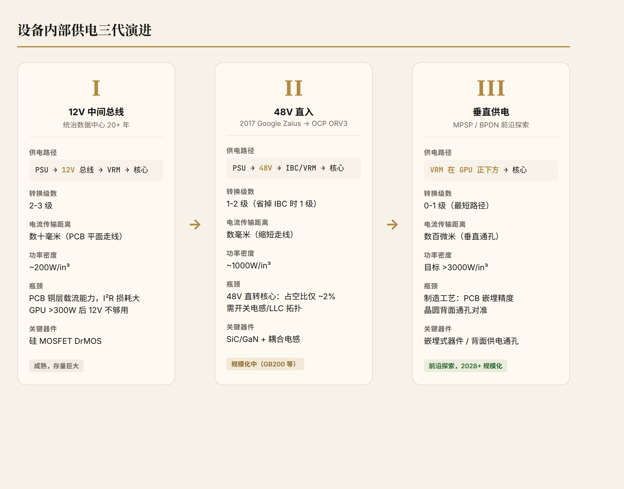
| Dimension | Generation 1 (12V Intermediate Bus) | Generation 2 (48V Direct) | Generation 3 (Vertical Power Delivery) |
|---|---|---|---|
| Power Delivery Path | 12V Bus → VRM → Core | 48V Direct → VRM → Core | VRM directly below/on backside of chip |
| Conversion Stages | 2-3 stages | 1-2 stages | 0-1 stages (Shortest path) |
| Current Transmission Distance | Tens of millimeters (PCB plane) | A few millimeters (Shortened traces) | Hundreds of microns (Vertical vias) |
| Power Density | ~200W/in³ | ~1000W/in³ | Target >3000W/in³ |
| Primary Bottleneck | PCB copper layer current-carrying capacity | VRM duty cycle optimization | Manufacturing process (Wafer-level/PCB embedding) |
| Maturity | Mature, massive installed base | Scaling up (GB200, etc.) | Frontier exploration, scaling in 2028+ |
| Key Components | Silicon MOSFET DrMOS | SiC/GaN + Coupled inductors | Embedded devices / Backside vias |
| Chinese Participation | High (Huawei, Inspur, etc. all have design capabilities) | Medium (Innoscience GaN, Silan Microelectronics DrMOS) | Low to Medium (Foundation in PCB embedding, lagging in wafer-level) |
800V and 48V Are Not Mutually Exclusive
This is a common point of confusion. Let's clarify:
- 800V DC solves the facility side, from the grid to the rack entrance. It replaces AC power distribution (415V AC + UPS + PDU)
- 48V Direct solves the in-device side, from the rack entrance to the GPU board. It replaces the 12V intermediate bus
- The two are different segments of the same chain and do not conflict. The complete path:
13.8kV AC → SST → 800V DC → Sidecar DC-DC → 48V → VRM → GPU (0.8-1.2V)
                                        ↑ Facility Side  ↑ In-Device
                                     800V Range        48V Range
NVIDIA's 800V architecture whitepaper explicitly states: the Sidecar outputs 48V DC, and then 48V enters the compute tray, where board-level VRMs complete the final step-down. 800V delivers power to the door, 48V delivers power to the desk, and vertical power delivery puts it right in your hand. It's a three-stage relay, each with its own technical challenges.
Where the $27 Billion Comes From: Breaking Down the Rack into Individual Chips
Bank of America's bottom-up demand model is the most valuable part of this report. Instead of simply providing a TAM (Total Addressable Market), they break down the semiconductor content at every power distribution stage within the AI data center to calculate it:
Single Rack Analog Semiconductor Content Value:
| Rack Power Level | Analog Semiconductor Content | Corresponding Platform |
|---|---|---|
| ~15 kW (Traditional) | ~$36,000 | Traditional servers |
| ~120 kW | — | Blackwell |
| ~600 kW | ~$300,000 | Rubin Ultra |
| ~1,500 kW (1.5 MW) | >$900,000 | Feynman |
The analog chip content in a megawatt-class rack approaches one million dollars—the power devices, power management ICs, driver ICs, current sensors, and protection circuits within each rack add up to far more than most people imagine.
Aggregated to Market Size:
| Metric | 2025 | 2030 | CAGR |
|---|---|---|---|
| AI Data Center Analog Semiconductor TAM | $7.9 billion | $27 billion | 28% |
| AI Data Center New Power Demand | ~17 GW/year | ~60 GW/year | — |
A 28% CAGR represents rapid expansion in the semiconductor sector. Moreover, this growth is not cyclical—it follows AI compute deployment; as long as GPU power consumption continues to rise, the semiconductor content in power distribution architectures will keep climbing.
The biggest beneficiary direction: SiC (Silicon Carbide) and GaN (Gallium Nitride). These two wide-bandgap semiconductor materials are accelerating their migration from cyclical automotive/industrial demand to the long-term structural demand of AI data centers.
Why SiC and GaN
Traditional silicon-based power devices fall short in 800V/megawatt-class scenarios—their breakdown voltage, conduction losses, and switching frequencies are insufficient. Wide bandgap semiconductors are not just an enhancement, but a necessity for implementing the 800V architecture:
SiC handles the high-voltage front-end:
- Rated voltage above 1200V, performing the primary conversion from medium-voltage AC to 800V DC at the data center's main power input stage
- Higher maturity than GaN, making it the preferred choice for the data center input side
- Infineon CoolSiC, onsemi EliteSiC, and STMicroelectronics STPOWER are the current mainstream product lines
GaN handles high-density in-rack conversion:
- Switching frequencies can reach the MHz range, allowing for smaller inductors and capacitors
- Power density of GaN-based converters has exceeded 4.2 kW/L, enabling efficient step-down conversion from 800V DC to the 12V required by the GPU
- Device volume is only 1/5 that of silicon-based solutions; in high-density racks, space is compute
The two are not in competition, but complementary: SiC handles high power at the input, while GaN handles high density at the point of load. A data center requires both.
China's Position: Further Ahead Than You Think
This is the most easily underestimated part in domestic media and industry reports. Most people know the positions of Infineon, TI, and onsemi in the power semiconductor field, but China has secured several key positions in the 800V data center power distribution industry chain.
Innoscience: The Sole Chinese Chip Supplier in NVIDIA's 800V Ecosystem
On August 1, 2025, NVIDIA's official website updated its list of partners for the 800V DC power architecture, and Innoscience (HKEX: 02577) was selected, making it the only Chinese chip company on the list.
Innoscience's positioning is to provide an end-to-end GaN power solution for the NVIDIA Kyber rack system. Its inclusion is not due to political balancing, but rather technical strength:
- Full IDM autonomy: From substrate, epitaxy, and chip design to packaging and testing, everything is self-developed. The yield rate of the 8-inch silicon-based GaN mass production line exceeds 95%
- Full voltage coverage: GaN devices cover 15V to 1200V, adapting to every link from rectification to end-point voltage regulation on the 800V DC power distribution chain
- Efficiency data: Third-generation GaN devices achieve an efficiency of 98.5%, reducing losses by about 30% compared to traditional silicon-based solutions
- World's only 8-inch GaN mass production: While competitors are still at 6 inches, Innoscience has successfully ramped 8 inches, showing clear advantages in cost and capacity
On the day the news was released, Innoscience's Hong Kong stock surged as much as 64% intraday. This is not emotional speculation; NVIDIA's supplier qualification is extremely strict, and being selected means the technical specifications have passed the actual testing and verification of NVIDIA's engineering team.
SiC Direction: StarPower Semiconductor, Silan Microelectronics, Sanan Optoelectronics
The core segments of the SiC industry chain are substrates and epitaxy (accounting for about 70% of device cost), which have the highest technical barriers.
| Company | Positioning | Progress |
|---|---|---|
| Sanan Optoelectronics | China's only 6-inch SiC full industry chain (substrate + epitaxy + device) IDM | Mass produced, 8-inch R&D advancing |
| SICC | SiC substrate, technology roadmap benchmarked against Wolfspeed | 6-inch conductive substrates in mass shipment |
| StarPower Semiconductor | IGBT/SiC modules, automotive-grade verification | Expanding into industrial and data centers |
| Silan Microelectronics | Three-pronged approach: silicon-based + SiC + analog | DrMOS, eFuse, and other AI server power chip combos partially mass-produced |
There is still a gap in maturity compared to Infineon and STMicroelectronics. International leading companies took the lead in promoting 8-inch SiC mass production, while Chinese companies are still transitioning from 6-inch to 8-inch. However, the gap is narrowing, and 800V data centers are a brand-new field where everyone faces similar technical challenges, meaning less historical baggage.
Power Systems and Integration: Delta Electronics, Megmeet, Chipown
Chips are the foundation, but the ultimate implementation of 800V power distribution relies on power modules and system integrators. Chinese companies have a clear advantage in this direction:
| Company | Role | Key Information |
|---|---|---|
| Delta Electronics | Member of NVIDIA 800V HVDC supplier alliance | Global data center power module market share exceeds 15%, single PSU power reaches 27.5kW, efficiency 98%+ |
| Megmeet | NVIDIA official partner directory | Power module supplier, collaborating with NVIDIA to develop 800V HVDC solutions |
| Chipown | AI data center power chips | 1700V SiC auxiliary power solution, multi-phase VRM, high-frequency digital power controller |
| Envicool / Shenling Environment | Liquid cooling + power distribution integration | High-density power distribution and thermal dissipation collaborative design |
Delta Electronics is a crucial player in NVIDIA's 800V ecosystem. It does not produce chips, but performs system-level integration, turning chip capabilities into deliverable power modules. In the global data center power market, Delta's share is just like Infineon's chip share—an infrastructure-level player.
Industry Chain Panorama: Who is in Which Segment
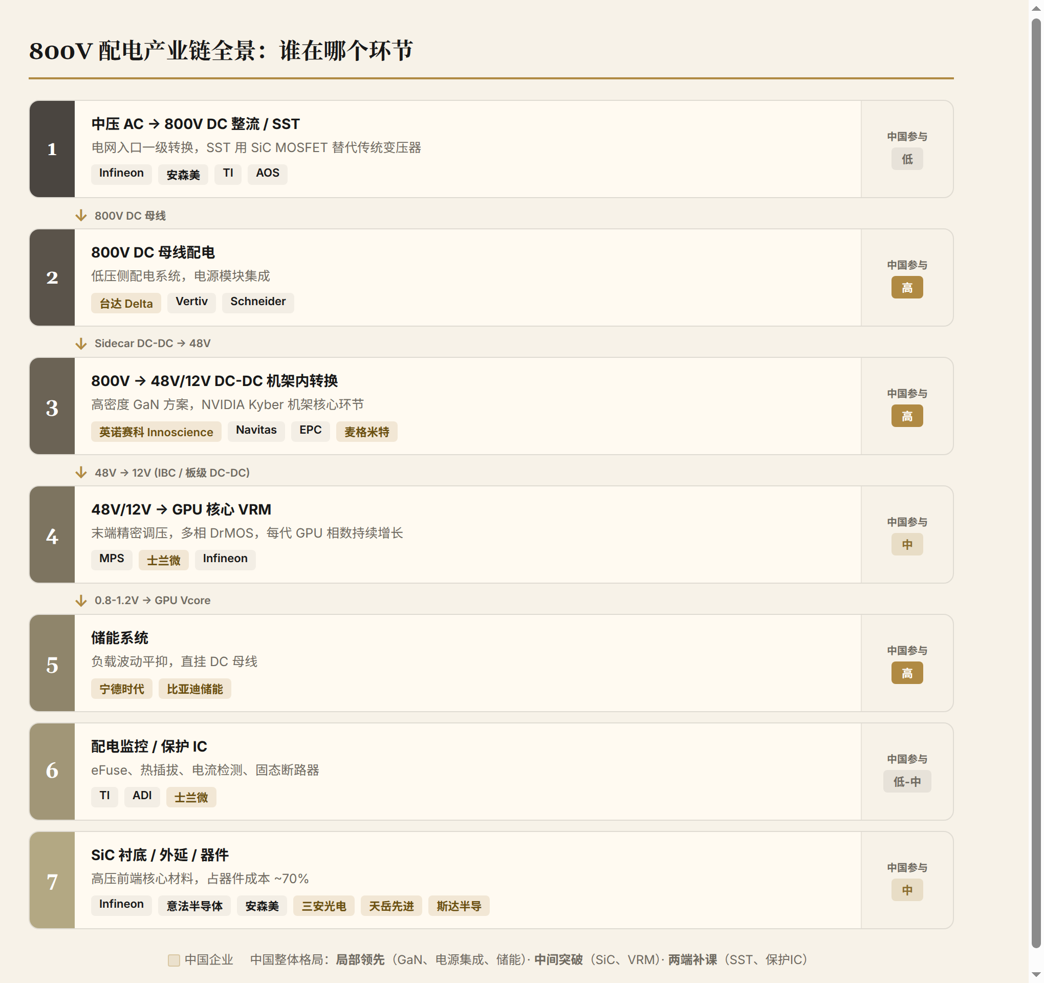
Mapping out the complete 800V power distribution link from the grid to the GPU, the main players in each segment are as follows:
| Segment | Function | Main Players | Chinese Participation |
|---|---|---|---|
| Medium Voltage AC→800V DC Rectification/SST | Grid entry first-stage conversion | Infineon, onsemi, TI, AOS | Low (Participating in SiC substrates, just starting in devices) |
| 800V DC Busbar Power Distribution | Low-voltage side power distribution | Vertiv, Schneider, Delta Electronics | High (Delta Electronics is a core supplier) |
| 800V→50V/12V DC-DC | In-rack high-density conversion | Innoscience (GaN), Navitas, EPC | High (Innoscience is NVIDIA's only Chinese GaN supplier) |
| 50V/12V→GPU Core VRM | Terminal precision voltage regulation | MPS, Silan Microelectronics, Infineon | Medium (Silan Microelectronics has entered, but overall share is still small) |
| Power Module/PSU | System integration | Delta Electronics, Megmeet, Flex Power | High |
| Energy Storage System | Load fluctuation smoothing | CATL, BYD Energy Storage | High (Batteries are China's absolute advantage area) |
| Power Distribution Monitoring/Protection IC | Current sensing, eFuse, hot-swap | TI, ADI, Silan Microelectronics | Low to Medium |
Mapping out the entire link reveals that China's participation in 800V power distribution is not a "comprehensive catch-up," but rather "local leadership, mid-stream breakthroughs, and catching up at both ends." GaN devices (Innoscience) and power system integration (Delta Electronics, Megmeet) already possess global competitiveness; SiC substrates and epitaxy are catching up; while there is still a gap in entry-side high-voltage devices and precision protection ICs.
Several Noteworthy Judgments
Returning to Huang's five-layer framework: energy → chips → infrastructure → models → applications. Innovation in the top four layers is accelerating, but the physical constraints of the energy layer don't disappear just because your software gets better. The judgments below all rest on this fundamental asymmetry—the faster the upper layers innovate, the more painful the bottom-layer bottleneck becomes.
1. 800V DC Penetration May Exceed Expectations
Bank of America predicts that by 2030, 78% of new data center capacity will adopt 800V DC. This figure looks aggressive, but the logic is solid: it's not a matter of technology preference, but rather that megawatt-class racks have no other physically viable solutions. When the power consumption of a Rubin Ultra rack exceeds 600kW, 54V is an engineering dead end. 800V isn't just "a bit better"; it's "the only way."
2. Analog Chips Are Not Bottlenecked by Process Nodes Like Digital Chips
This is an important structural assessment. GPUs are constrained by advanced process nodes, but power devices and analog ICs primarily use mature processes (65nm to 280nm), falling outside the restrictions of EUV lithography machines. The bottlenecks for SiC and GaN lie in material growth and device design, not in lithography precision.
This means China's path for domestic substitution in the analog/power semiconductor sector is shorter than for digital chips. Innoscience has already proven this: without advanced EUV, a fully autonomous IDM supply chain can still produce products recognized by NVIDIA.
3. But There's a Hidden Concern: The Industry Landscape Favors "Point Solutions" Over "Comprehensive Portfolios"
China's current positioning is more like having star enterprises at specific nodes (Innoscience in GaN, Delta Electronics in power modules), but lacking a complete product line covering power + analog + protection like Infineon or TI. In NVIDIA's 800V ecosystem, Chinese companies provide key components, not complete solutions.
From a commercial perspective, this is both an opportunity and a risk. The 800V architecture demands extremely high supply chain reliability, and NVIDIA will tend to choose suppliers that can provide full-link support. If Chinese companies can only produce single-point components and cannot do system integration, their long-term value ceiling will be suppressed.
4. SST (Solid-State Transformer) is the Next Technological Watershed
Current 800V DC implementation solutions still rely on traditional transformers for medium-voltage AC to 800V DC conversion. The true ultimate form is SST, using power electronic devices to replace transformers, converting 13.8kV AC directly to 800V DC in a single stage, pushing efficiency from 97% to 98.5%.
The core devices of SST are high-voltage SiC MOSFETs and digital control ICs. This segment is currently entirely the territory of Infineon, onsemi, and TI, with very low participation from Chinese companies. If SST begins scaled deployment after 2028 (NVIDIA's roadmap implies this timeline), a new divergence in the competitive landscape will emerge here.
Data Cross-Validation and Uncertainties
Verified Core Data:
- NVIDIA 800V DC whitepaper exists and is public (released at OCP in October 2025)
- Innoscience listed in NVIDIA's official supplier directory (verifiable on NVIDIA's website as of August 1, 2025)
- Delta Electronics and Megmeet are members of the NVIDIA HVDC supplier alliance
- Bank of America report published on May 25, 2026; core data is cross-verifiable
Data Requiring Independent Confirmation:
- Bank of America's $7.9B→$27B TAM model assumptions (full methodology not seen; may be overly optimistic regarding 800V penetration rate assumptions)
- The forecast that "78% of new data center capacity will adopt 800V DC" by 2030—this figure is disputed in the industry; some analysis firms consider 30-50% more realistic
- Single-rack analog chip content "exceeding $900K"—this may be a peak configuration (Feynman platform); actual deployments may use mixed solutions to reduce costs
Key Uncertainties:
- Whether the Feynman platform's power consumption can truly reach 1.5MW—this is still in the product planning stage
- Timeline for large-scale commercialization of SST—currently still in the demonstration stage
- Potential impact of geopolitical factors on NVIDIA's supply chain choices
Observation Points
Several events worth tracking next:
- COMPUTEX 2026 (June 1-5): NVIDIA may update the commercialization progress of its 800V architecture during Jensen Huang's keynote
- Rubin Ultra mass production timeline: This is the trigger for 800V HVDC to transition from "planning" to "deployment"
- Innoscience's actual supply share in the NVIDIA Kyber rack—making the vendor list and securing large orders are two different things
- Domestic SiC 8-inch production line progress: Whether Sanan Optoelectronics, SICC, and others can achieve mass production by 2027
Data sources: Bank of America Securities "Watts to Tokens" report (May 25, 2026); NVIDIA 800VDC Architecture white paper (October 2025); public news reports and company announcements. Market size data is from the BofA research report; inferences not independently verified are noted in the text.