The Interconnect Bet Behind China's AI Compute Breakout
Draft v0.2 | 2026-05-30
1. Why Lingqu Is Needed
The competition in AI compute has shifted from "who has the faster chip" to "who can glue more chips together."
The reason is straightforward: single-chip compute growth is slowing, but training parameter counts double every 18 months. GPT-4 has roughly 1.8 trillion parameters, and under MoE architecture, only a fraction are activated per inference. This means the frequency and bandwidth demands of All-to-All communication are growing explosively. The efficiency of all three parallelism strategies — Tensor Parallelism (TP), Expert Parallelism (EP), and Pipeline Parallelism (PP) — depends directly on interconnect bandwidth and latency.
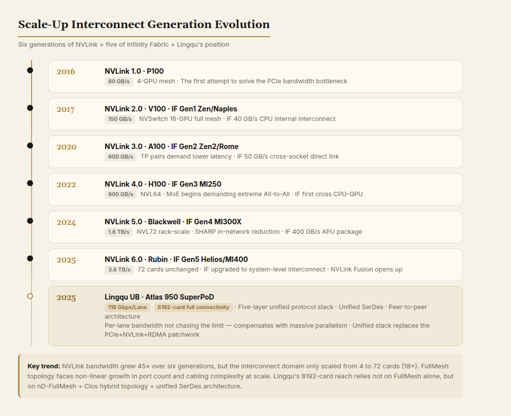
In September 2025, Huawei unveiled the Atlas 950 SuperPoD at the Ascend Developer Conference: 8,192 Ascend NPUs in a non-blocking full-mesh, with single-cluster compute rivaling NVIDIA's DGX SuperPOD. The backbone of this system is neither PCIe, nor NVLink, nor RoCE — it's a unified interconnect protocol Huawei built from scratch: Lingqu (UnifiedBus, or UB).
Against this backdrop, the interconnect protocol landscape looks like this:
- PCIe: A general-purpose I/O bus. PCIe 5.0 x16 delivers 128 GB/s bidirectional; PCIe 6.0 roughly doubles that to ~242 GB/s. But its evolution can't keep pace with GPU compute growth, and the protocol stack itself adds hundreds of nanoseconds of overhead.
- NVLink: NVIDIA's proprietary protocol. Fifth-generation delivers 1.8 TB/s bidirectional, but it only works between NVIDIA's own chips and isn't available to outsiders.
- InfiniBand/RoCE: Network-level interconnects with microsecond-scale latency, suitable for cross-node communication but unable to meet the nanosecond-scale demands of shared memory between GPUs within a node.
- CXL: A cache-coherent protocol built on PCIe physical layer. CXL 3.x supports memory pooling, but bandwidth is constrained by PCIe lane count, and ecosystem maturity is limited.
China faces an additional constraint: process technology restrictions mean weaker single-chip compute. The Ascend 950PR delivers roughly 60-70% of H100's per-card compute, but the Atlas 950 SuperPoD matches or even exceeds some NVIDIA solutions in overall system throughput by leveraging 8,192 cards in a non-blocking full mesh. This is what Huawei calls "using math to compensate for physics, non-Moore to supplement Moore": leveraging interconnect advantages to offset single-chip shortcomings.
Lingqu is the core infrastructure of this strategy.
2. What Is Lingqu
Let's get Lingqu's positioning straight before discussing why it's designed this way.
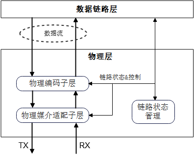
Lingqu is a unified interconnect protocol designed for SuperNodes. Its goal is to replace multiple interconnect technologies — PCIe, NVLink, C2C, RoCE, and others — with a single protocol stack covering all interconnect scenarios, from intra-chip to intra-cluster.
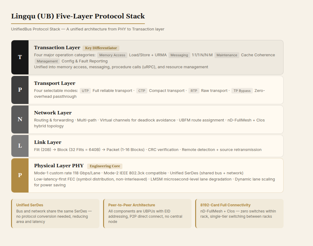
2.1 The Five-Layer Protocol Stack
Lingqu's protocol stack is divided into five layers, each with clear responsibilities and flexible composability:
Physical Layer (PHY)
The physical layer provides two modes:
- PHY Mode-1: Custom data rates, currently 118 Gbps/Lane, exceeding the same-generation IEEE Ethernet standard rate. Based on SerDes DSP + FEC + linear direct-drive technology.
- PHY Mode-2: Compatible with Ethernet physical layer, able to share Ethernet's optical module and cabling ecosystem.
The physical layer supports multiple FEC (Forward Error Correction) modes, flexibly selectable based on link quality. It also supports dynamic lane scaling: if a lane fails, the system can downshift without interrupting service, combined with N+N optical module redundancy for hardware-level fault tolerance.
Link Layer (LINK)
Based on Flit (Flow Control Unit) transmission. A Flit is the minimum link-layer transmission unit. 32 Flits form a Block, and 1-16 Blocks form a Packet. The link layer handles CRC verification and optional link-layer retransmission. When the remote end detects packet loss, it sends a retransmission request to the source, completing error correction at the link layer — transparent to upper layers.
Network Layer (NETWORK)
Responsible for routing and forwarding. The Lingqu network layer supports multipath routing, combined with virtual channel technology to avoid deadlocks. Within a SuperNode, all UBPUs (Lingqu Processing Units) receive routing information allocated by the UBFM (Lingqu Bus Fabric Manager).
Transport Layer (TRANSPORT)
The transport layer provides three modes, flexibly chosen per scenario:
- UTP (UB Transport Protocol): Full transport layer, providing reliable delivery guarantees.
- CTP (Compact Transport Protocol): Streamlined transport layer, reducing overhead.
- RTP (Raw Transport Protocol): Bare transport layer, minimizing protocol overhead.
There's also a TP Bypass mode that can completely skip the transport layer in certain scenarios, further reducing latency. This flexibility is a hallmark of Lingqu: not all communications need full transport-layer guarantees. For latency-sensitive synchronous memory accesses, Bypass mode can significantly reduce protocol stack overhead.
Transaction Layer (TRANSACTION)
The transaction layer defines four major operation categories:
- Memory Accessing: Read/write between UBPUs, supporting both synchronous Load/Store semantics and asynchronous URMA (Unified Remote Memory Access) semantics.
- Message Passing: Supporting 1-to-1, 1-to-many, many-to-1, and many-to-many message transmission.
- Maintain: Updating internal state of remote UBPUs, such as cache coherence maintenance and security state updates.
- Management: Status reporting during configuration and runtime, such as address assignment and fault reporting.
The transaction layer's design philosophy is to unify all user operations into four categories — memory access, message passing, procedure calls (uRPC), and resource management — providing efficient programming that directly leverages hardware capabilities. A single protocol stack supports all operations, avoiding protocol conversion overhead.
2.2 Peer-to-Peer Architecture
This is the most fundamental difference between Lingqu and traditional interconnects.
In traditional architectures, the CPU is the center. GPUs, NICs, and SSDs are all "devices" hanging off the PCIe bus, managed by the CPU. GPU-to-GPU communication must pass through the CPU as an intermediary, or rely on private high-speed channels like NVLink.
Lingqu flips this model entirely: all components are UBPUs (Lingqu Processing Units), with completely equal status.
Each UBPU has:
- EID (Entity ID): A globally unique identifier, serving a role similar to an IP address.
- UMMU (UB Memory Management Unit): A hardware-level memory authentication and address translation module that translates global UBA (UB Address) to local physical addresses.
- UB Controller: The hardware implementation of the protocol stack, interfacing directly with the compute unit's NoC (Network-on-Chip).
UBPUs can directly initiate Load/Store or URMA operations to access each other's memory without going through any intermediate node. Communication covers all combinations — H2H (CPU-to-CPU), H2D (CPU-to-NPU), D2D (NPU-to-NPU), H2N (CPU-to-DPU), H2S (CPU-to-SSU) — and works the same way across nodes and across racks.
UBFM (UB Fabric Manager) manages EID allocation, routing configuration, and resource management across the entire Fabric domain, but it only handles management — never data forwarding. The data path is fully decentralized.
2.3 Unified Programming Model
Lingqu provides two programming interfaces:
- POSIX Interface: Applications adapt seamlessly; existing Linux programs require no modification.
- High-level Service API: Provided through openEuler's UB Service Core, including pooled memory management (UBS Mem), communication services (UBS Comm), I/O services (UBS IO), compiler and runtime (UBS Compiler & Runtime), virtualization (UBS Virt), and Serverless (UBS Serverless).
At the hardware level, the UB Controller natively matches the out-of-order and concurrent execution characteristics of compute units. Compute units can directly schedule the UB Controller via instructions, without additional driver-layer intervention.
2.4 Full Resource Pooling
Lingqu supports comprehensive pooling of compute, storage, and interconnect resources within a SuperNode:
- Compute Resource Pooling: Multi-tenant security isolation through UB Partition, with microsecond-level resource sharing and migration.
- Interconnect Resource Pooling: All Entities can use all reachable paths and ports, achieving TB/s-level bandwidth pooling through multi-channel sharing.
- Storage Resource Pooling: Remote SSUs (Storage Server Units) expose storage resources directly through UB, accessed via MMIO and messaging.
Pooled resources are managed centrally by UBFM, but the data path remains decentralized P2P direct connect.
2.5 Large-Scale Networking
Lingqu supports linear scaling from 64 to 8,192 cards, using an nD-FullMesh + Clos hybrid topology strategy:
- Intra-Rack: 1D/2D-FullMesh topology, direct cable connections, zero switches, providing high local bandwidth.
- Inter-Rack: Single-tier Clos topology. Each rack embeds a UB Switch; cross-rack interconnection uses 25.6T switches.
Take Atlas 950 as an example: a single rack has 64 NPUs + 4 CPU boards + 1 standby board, with 16 Lane × 64 Port providing full mesh. 128 racks form an 8,192-card SuperNode, with single-tier Clos switching between racks.
Lingqu also supports two converged networking modes:
- UBoE (UB over Ethernet): UB protocol carried over Ethernet physical layer, interfacing with Ethernet switches. IANA has assigned UB hardware type (38) and dedicated port (4792).
- UB + OCS: Working with optical circuit switches to enable variable topologies that match dynamic business traffic.
2.6 High Availability
Lingqu's reliability design is layered:
- Physical Layer: Dynamic lane scaling + N+N optical module redundancy. No service interruption under single-point failure.
- Link Layer: Remote retransmission mechanism. Link flaps and bit errors are transparent to upper layers.
- Transport Layer: End-to-end reliable transport (UTP mode).
- Management Plane: UBFM real-time monitoring, automatic fault isolation, and path rerouting.
The overall target is microsecond-level fault detection and recovery, transparent to applications.
3. Understanding Lingqu's Design Motivation Through the CUDA-NVLink Evolution
Now that we understand Lingqu's architecture, the next question is: why "invent a new protocol"? The answer lies in NVLink's evolution.
3.1 How CUDA Forced NVLink Into Existence
To understand why Lingqu needed to "invent a new protocol," we first need to understand why NVLink exists.
Before 2014, GPU-to-GPU communication had only one path: PCIe. PCIe was a bus protocol Intel designed in the 1990s for general-purpose I/O — it was never designed for the high-frequency, high-bandwidth, low-latency data exchange between GPUs. As CUDA transformed GPUs from graphics accelerators into general-purpose compute engines, communication volumes between GPU clusters exploded, and PCIe's bandwidth bottleneck became the ceiling for the entire system.
Every generation of NVLink evolution was CUDA's programming model forcing interconnect design forward:
- NVLink 1.0 (2016, P100): 80 GB/s bidirectional, 5× PCIe 3.0. Solved GPUDirect P2P bandwidth, but could only connect 4 GPUs in a simple mesh topology.
- NVLink 2.0 (2017, V100): 150 GB/s, introduced NVSwitch for 16-GPU full mesh. CUDA Unified Memory began relying on NVLink for transparent cross-GPU memory access.
- NVLink 3.0 (2020, A100): 600 GB/s, major bandwidth increase but topology unchanged. CUDA's Tensor Parallelism began demanding predictable low latency from NVLink.
- NVLink 4.0 (2022, H100): 900 GB/s, NVL64 emerged. CUDA's MoE support started placing extreme demands on All-to-All communication.
- NVLink 5.0 (2024, Blackwell): 1.8 TB/s, NVL72 rack-level full mesh. SHARP engine provides in-network reduction acceleration.
- NVLink 6.0 (2026, Rubin): 3.6 TB/s. NVL72 remains at 72 cards, but bandwidth doubles.
Notice a critical trend: NVLink's scale ceiling hasn't grown in step with bandwidth. From NVL64 to NVL72 is only a 12.5% increase, while bandwidth grew 4× from 900 GB/s to 3.6 TB/s. This isn't because NVIDIA doesn't want larger scales — it's because NVLink's FullMesh topology hits physical bottlenecks at large scales: 72 GPUs in full mesh requires 72×71/2 = 2,556 links. The switch chip port counts and cabling complexity are approaching engineering limits.
NVIDIA's solution is to layer NVSwitch on top of NVLink for switched interconnect, but switched interconnect introduces extra hops and latency. NVL72 uses one tier of NVSwitch; larger scales require two or even three tiers, with latency and cost scaling non-linearly.
3.2 CUDA's Three Hard Requirements for Interconnect
NVIDIA's decade of interconnect evolution is driven by three hard requirements from the CUDA programming model:
Requirement One: Global Memory Visibility. CUDA Unified Memory lets developers access any GPU's memory as if it were local. Under the hood, NVLink provides hardware-level address translation and page migration. This capability makes Tensor Parallelism for large models possible — model parameters are distributed across different GPUs, but compute cores access them through a unified address space.
Requirement Two: Nanosecond-Scale All-to-All Latency. Every inference in MoE architecture requires expert routing (All-to-All communication). Take DeepSeek V4: a 1.6-trillion-parameter MoE model where each inference requires reading from 256 experts on different GPUs. If All-to-All latency increases from 100 nanoseconds to 10 microseconds, inference throughput drops by over 50%.
Requirement Three: Predictable Bandwidth Isolation. When training and inference are co-deployed, bandwidth demands vary enormously across tasks. Tensor Parallelism requires sustained high-bandwidth All-Reduce, while MoE inference needs high-frequency small-message All-to-All. If both share the same set of links, bandwidth contention causes latency jitter.
3.3 Lingqu's Design Motivation: Starting from NVLink's Bottlenecks
When Huawei designed Lingqu, it faced a different set of core constraints from NVIDIA:
-
Process-constrained, weaker single-chip compute: The Ascend 950PR delivers roughly 60-70% of H100's per-card compute. To match equivalent system throughput, more chips must be glued together, requiring a larger interconnect scale than NVLink.
-
Can't use NVLink: Export controls eliminated the possibility of using NVLink, necessitating a homegrown interconnect.
-
Ecosystem built from scratch: Without a mature programming model like CUDA to lean on, the interconnect protocol must define memory semantics, programming models, and communication libraries itself.
These three constraints combined drove Lingqu's core design choices:
Why a unified protocol stack instead of layered assembly?
NVLink can afford to "only handle high-speed GPU-to-GPU channels" because it has PCIe underneath for CPU-GPU connections and InfiniBand above for inter-node communication. NVLink only needs to solve one problem: "how do GPUs quickly exchange data with each other."
Huawei doesn't have that luxury. It needs to build the entire interconnect system from scratch. If it went with a layered approach of PCIe + custom high-speed link + RDMA, each layer would need separate development and optimization — a massive engineering effort with inter-layer protocol conversions introducing uncontrollable latency. The unified protocol stack costs higher complexity, but the benefit is precise control over latency and bandwidth from physical layer through transaction layer.
Why an 8,192-card full-mesh scale?
This isn't about blindly chasing scale. The reason: weaker per-card compute means more cards are needed for the same training task. If NVLink's 72 cards correspond to the compute of 8×H100, Lingqu might need 200-300 Ascend cards to deliver equivalent compute. An 8,192-card interconnect scale means a single SuperNode can host multiple such training tasks, or complete a single ultra-large training task without cross-SuperNode communication.
Cross-SuperNode communication (Scale-Out) latency is in the microsecond-to-millisecond range, three orders of magnitude higher than the ~100-nanosecond range within a SuperNode. Reducing the proportion of cross-SuperNode communication is the core motivation behind Lingqu's pursuit of large-scale interconnect.
Why 118 Gbps/Lane instead of higher speeds?
NVLink 6's 224 Gbps/Lane requires SerDes built on sub-4nm processes and consumes enormous power. Huawei's SerDes expertise doesn't match NVIDIA's (NVIDIA can leverage TSMC's most advanced processes). Choosing 118 Gbps is a result of engineering feasibility tradeoffs.
But Lingqu compensates for per-lane bandwidth limitations through large-scale FullMesh topology: at 8,192 cards, the available paths between any two UBPUs far exceed NVLink's 72-card topology. Multipath transmission can aggregate bandwidth — individual links may be slower, but total available bandwidth can be very high.
The limitation of this design: Multipath transmission means out-of-order arrival, requiring reordering buffers at the receiver. This adds latency (reordering wait time) and area overhead (buffer size scales quadratically with path count). At 8,192-card scale, the number of paths could reach hundreds, and reordering buffer overhead becomes non-negligible.
3.4 Design Tradeoffs in Memory Semantics
Lingqu provides both Load/Store (synchronous) and URMA (asynchronous) memory access semantics. This design requires understanding the problem it solves.
The value of Load/Store: Lets compute cores directly access remote memory via instructions, without going through the OS or drivers. In MoE inference, expert routing needs to read small 64B-4KB data blocks from remote GPUs. Using traditional RDMA (which requires PIN-registered memory, submitting work requests, polling for completion), a single access takes 3-5 microseconds. With direct Load/Store access, this latency can be reduced to ~100 nanoseconds.
The value of URMA: Large-block data transfers (e.g., model parameter synchronization, All-Reduce). URMA is similar to RDMA but integrated within the protocol stack, eliminating the need for a separate RDMA NIC. This removes the torturous path of traditional architectures: "GPU → PCIe → CPU memory → RDMA NIC → network → remote NIC → remote CPU memory → remote PCIe → remote GPU."
The implementation cost:
Load/Store's synchronous semantics require the UMMU (UB Memory Management Unit) to maintain global address mappings at the hardware level. An address space of 8,192 UBPUs means the UMMU's page tables could be enormous. If each UBPU has 64 GB of HBM, the total global address space reaches 512 TB. The UMMU must complete lookups and translations across this address space at nanosecond scale, requiring extremely high TLB hit rates and carefully designed page table structures.
The thornier issue is coherence. The Lingqu specification doesn't explicitly state whether it supports Cache Coherence. If it doesn't, data accessed via Load/Store from a remote node might not be up to date — writes might still be in the remote cache and not flushed to main memory. Developers would need to manually manage cache flushes (similar to __threadfence_system() in GPU programming), significantly increasing programming complexity.
NVLink began supporting hardware cache coherence between GPUs starting from the fourth generation. This was a problem NVIDIA took two product generations to solve. Whether Lingqu can ensure correctness through software without coherence, or implement hardware coherence in a future version, is a key engineering challenge.
3.5 Lingqu vs. Existing Layered Systems: Not About Replacement
A table shows the positioning differences between Lingqu and existing interconnect protocols:
| Dimension | PCIe | NVLink | CXL | RDMA/RoCE | Lingqu |
|---|---|---|---|---|---|
| Design Goal | General I/O bus | High-speed GPU interconnect | Cache coherence + memory pooling | Remote memory access | Unified full-stack interconnect |
| Latency | Hundreds of ns | ~100 ns | ~100 ns | Microsecond-scale | 100 ns – μs |
| Bandwidth/Link | 64 GT/s (PCIe 6.0) | 224 Gbps (NVLink 6) | 64 GT/s (CXL 3.0) | 100-400 Gbps | 118 Gbps |
| Max Scale | 1 device/slot | 72 GPUs (NVL72) | Dozens of devices | Thousands of nodes | 8,192 UBPUs |
| Memory Semantics | DMA | Load/Store + DMA | Load/Store + Coherence | RDMA Read/Write | Load/Store + URMA |
| Cache Coherence | None | Supported between GPUs | Native support | None | Not specified |
Lingqu attempts to cover the capabilities of PCIe + NVLink + RDMA with a single protocol. The benefit is a unified programming model that eliminates protocol conversion. The cost is that each layer's performance falls short of dedicated solutions: Load/Store isn't as fast as NVLink (118 vs. 224 Gbps/Lane), RDMA semantics aren't as mature as dedicated RDMA NICs, and cache coherence remains unresolved.
Judgment: Lingqu's design is an engineering tradeoff of "trading peak performance for unification." For Huawei, this is the correct choice because its constraints don't allow the "use the best solution at each layer and stitch them together" approach. But for a vendor with access to NVLink, PCIe 6.0, and mature RDMA, Lingqu's unified protocol stack offers no clear performance advantage. Its competitiveness lies in large-scale networking (8,192 cards) and full-stack controllability, not in per-layer performance.
4. Domestic SuperNode Interconnect Route Competition
Lingqu didn't emerge from a vacuum. Its design choices only make sense in comparison. Let's look at the domestic landscape first, then the global one.
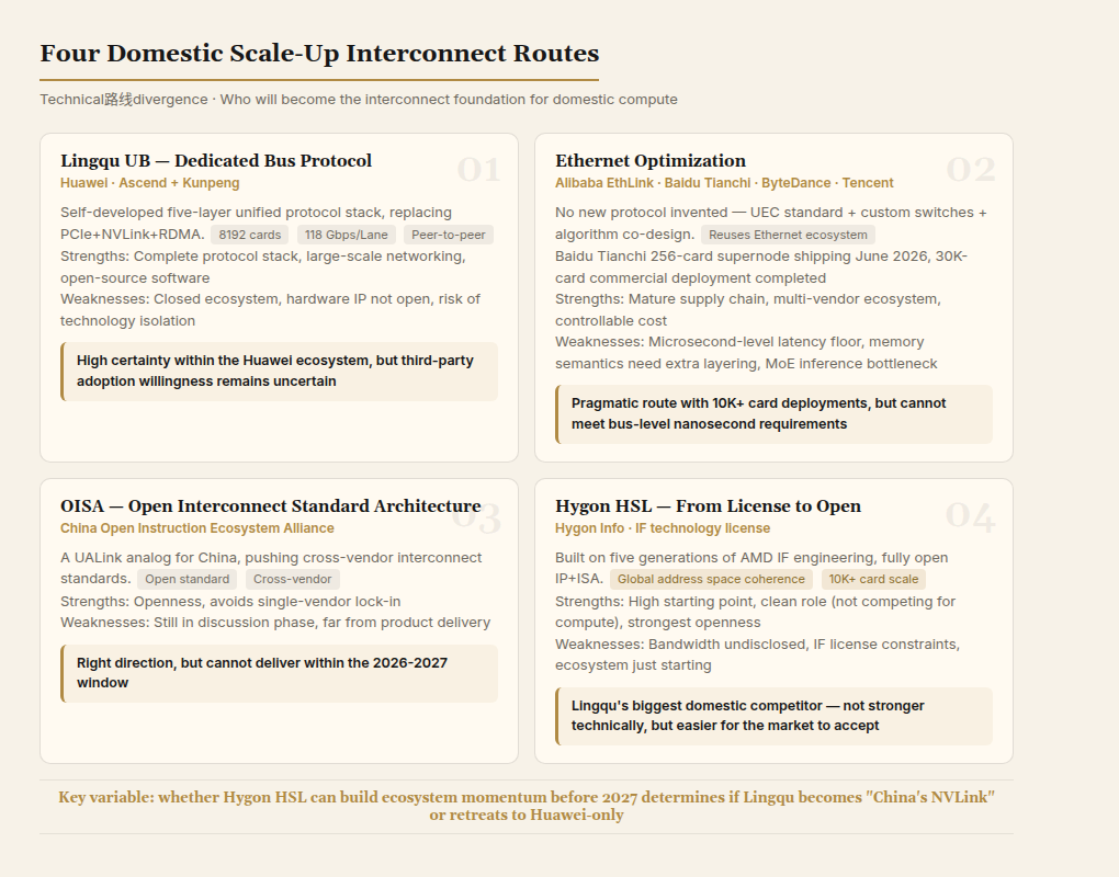
China has more than one path to AI SuperNode interconnect. By technology route, there are currently four main ones:
4.1 The Lingqu Route: Dedicated Bus Protocol
Representative: Huawei (Ascend + Kunpeng)
Core Approach: Self-developed unified protocol replacing PCIe/NVLink/RoCE across the full stack, using system-level interconnect advantages to compensate for single-chip shortcomings.
Advantages:
- Complete protocol stack design, unified from physical layer to application layer, with no protocol conversion overhead
- 8,192-card non-blocking full mesh, with clear performance advantages for large-scale training scenarios
- Open-source software stack (openEuler + openFuyao), lowering adaptation barriers
Disadvantages:
- Closed ecosystem — all core hardware IP comes from Huawei
- Third-party chipmakers' willingness and ability to integrate UB Controller remains unproven
- Incompatible with global mainstream technology routes (PCIe/CXL/UALink), creating technology island risk
4.2 The Ethernet Optimization Route
Representatives: Alibaba (EthLink/Eth-X), Baidu (Tianchi SuperNode), ByteDance, Tencent
Core Approach: Don't invent new protocols; instead, do deep optimization on Ethernet: Ultra Ethernet Consortium (UEC) standards + custom switches + algorithm-coordinated scheduling.
Baidu is the latest heavyweight entrant. In June 2026, the Tianchi 256-card SuperNode based on Kunlun P800 chips will officially launch, with a 512-card version following in H2. Tianchi features custom high-bandwidth switches, has completed commercial deployment of a 30,000-card cluster, and supports PD disaggregation inference. Baidu chose not to invent a new bus protocol — instead optimizing Ethernet for Scale-Up, following the same philosophy as Alibaba's EthLink.
Advantages:
- Leverages Ethernet's mature supply chain (optical modules, cables, switch ASICs), keeping costs low
- Multi-vendor ecosystem, avoiding single-supplier lock-in
- UEC standard is advancing rapidly, with large-scale commercial deployment expected by 2027
- Baidu Tianchi's deployment further proves: Ethernet is not just a paper proposal in China — it already has 10,000+ card commercial deployments
Disadvantages:
- Ethernet is fundamentally a network-level interconnect; its latency floor is in the microsecond range and can't reach bus-level ~100 ns
- Memory semantics and coherence require additional layers (e.g., CXL over PCIe), so the protocol stack remains layered
- For All-to-All-intensive MoE inference, latency may become a bottleneck
4.3 OISA (Open Interconnect Standard Architecture)
Representative: China Open Instruction Ecosystem Alliance
Core Approach: Promote an open interconnect standard, similar to a Chinese version of UALink. The goal is to establish a cross-vendor interconnect protocol standard.
Current Status: The standard is still in discussion. It's far from actual product deployment.
4.4 Hygon HSL: From Licensing to Openness
Representative: Hygon Information Technology
Hygon HSL's background must be understood starting from AMD's Infinity Fabric technology licensing.
Infinity Fabric's Technical DNA
Infinity Fabric (IF) is not a single interconnect protocol. It's a unified system interconnect architecture AMD spent nearly a decade building. Its evolution maps clearly to AMD's product strategy:
- IF Gen1 (2017, Zen/Naples): Emerged as intra-CPU interconnect, solving communication between multiple CCDs (Core Complex Dies). Link bandwidth ~40 GB/s, used for the dual-track Data Fabric and Control Fabric architecture within CPUs.
- IF Gen2 (2019, Zen 2/Rome): Bandwidth increased to ~50 GB/s, began supporting cross-socket (2P) direct CPU-to-CPU connection. AMD's strategy of gluing multiple Chiplets together with IF started paying off.
- IF Gen3 (2021, MI250/EPYC Milan-X): Critical upgrade. IF crossed from CPU to GPU for the first time — the two GPU dies in MI250 were directly connected via IF Gen3, sharing a memory address space. This laid the groundwork for MI300's CPU+GPU fused architecture. The Frontier supercomputer used IF Gen3 to achieve unified CPU-GPU memory access.
- IF Gen4 (2023, MI300X/EPYC Genoa): AMD used IF to package 8 GPU dies + 2 CPU dies in MI300, forming an "Accelerated Processing Unit (APU)." GPU and CPU share HBM memory, with IF Gen4 providing ~400 GB/s die-to-die bandwidth. This is the core of AMD's "unified memory architecture."
- IF Gen5 (2025, Helios/MI400): AMD evolved IF into "Infinity Architecture," repositioning from chip-level interconnect to system-level interconnect. The Helios rack-level platform uses IF Gen5 to connect EPYC Venice CPUs, MI400 GPUs, and Pensando Vulcano NICs into a unified rack-level system. It supports both UALink and Ultra Ethernet as external interfaces, with IF Gen5 serving as the internal interconnect "backbone."
IF's design philosophy is layered evolution, gradual expansion. From initial intra-CPU interconnect, to CPU+GPU intra-package interconnect, to system-level interconnect — each generation extends the previous one's functional scope rather than starting over. The cost of this incremental approach is heavier legacy baggage in the protocol stack, but the benefit is a foundation validated through large-scale deployment at every generation.
Hygon HSL's Technical Origins
In 2016, AMD and Tianjin Hygon signed a technology licensing agreement covering the Zen architecture CPU and partial GPU/interconnect technology. Hygon developed the C86 series CPUs and Deep Computing series DCUs on this foundation.
Hygon HSL (High-performance Scalable Link) genetically derives from the licensed version of IF, but with two key modifications:
-
Domestic adaptation: Added national cryptography algorithm instructions, security processors, and vulnerability defense mechanisms. These aren't cosmetic — security capabilities are embedded at the bus protocol level. HSL claims to support "global address space coherence," meaning all connected chips share a unified memory address space with hardware-level coherence guarantees.
-
Open strategy: In September 2025, Hygon officially opened the HSL 1.0 specification to the industry. This isn't simply "publishing documents" — it provides complete IP reference design and open instruction set, allowing other domestic chipmakers to directly integrate HSL interfaces. Vendors like Biren, SweiYuan, and Cambricon don't need to design interconnect protocols from scratch; they only need to integrate HSL IP to form heterogeneous systems with Hygon's CPUs/DCUs.
HSL's Five Key Features
Based on Hygon's public information, HSL's core features include:
- High Bandwidth: Far exceeding PCIe bandwidth (specific numbers undisclosed, but claimed to support 10,000-card heterogeneous interconnect)
- Low Latency: Bus-level direct connection, no network protocol stack traversal
- Global Address Space Coherence: All connected chips share a unified memory address space, hardware-guaranteed coherence
- Full-Stack Openness: Open bus protocol specification, IP reference design, and instruction set
- Flexible Scaling: From single-machine multi-card to large-scale AI compute clusters
Hygon's Strategic Intent
Hygon's goal in opening HSL isn't to compete with Lingqu over "whose protocol is better," but to do something Lingqu can't: become the unified interconnect standard for domestic chips.
Lingqu's problem: it's led by Huawei, and Huawei is both a supplier and a competitor. Other domestic chipmakers' concerns about Lingqu aren't technical — they're about "if I use your interconnect protocol, will you hold me by the throat in the next version?"
Hygon's positioning is different. Its CPUs use x86 architecture, and its DCUs are compatible with the CUDA ecosystem. It doesn't directly compete with GPU vendors like Biren or SweiYuan in the core compute market. Opening HSL is essentially saying: "Interconnect is my contribution; compute is your business." This role is inherently easier for other vendors to accept.
Moreover, HSL already has five generations of IF engineering as a foundation. Although Hygon hasn't disclosed the specific terms of the IF license (whether it restricts HSL's evolution direction), IF's maturity means HSL doesn't need to solve basic interconnect problems from scratch (cache coherence, deadlock avoidance, routing algorithms, etc.) and can focus engineering resources on domestic adaptation and ecosystem building.
HSL's Limitations
-
Bandwidth and speed undisclosed. Hygon hasn't published HSL's specific bandwidth parameters or lane speed, making quantitative comparison with Lingqu, NVLink, or UALink difficult. This could be a technical limitation (bandwidth falls short of competitors) or a business strategy (not exposing technical details).
-
Constraints of the IF license terms. AMD's licensing agreements typically have technical scope and usage restrictions. Whether Hygon can make breakthrough architectural innovations on HSL (like Lingqu's five-layer protocol stack) or can only make incremental improvements within the IF framework depends on the license terms. This information isn't public, so outsiders can't judge.
-
Ecosystem building has just begun. The HSL 1.0 specification was published in Q4 2025, and partnerships with ecosystem players are still in early stages. From specification release to product deployment typically takes 18-24 months, meaning HSL's actual impact won't be visible until 2027.
Judgment: HSL is Lingqu's most important competitor in the domestic market — not because HSL is technically superior, but because Hygon's "open interconnect provider" positioning is more acceptable to other domestic chipmakers than Huawei's "full-stack self-development + protocol publication" model. If HSL can attract enough ecosystem partners by 2027, it has a chance to become the de facto interconnect standard for domestic chips, while Lingqu may retreat to within the Huawei ecosystem.
5. International Competitive Landscape
Let's zoom out. Lingqu isn't addressing a China-specific problem — globally, everyone is tackling the same bottleneck: Scale-Up interconnect.
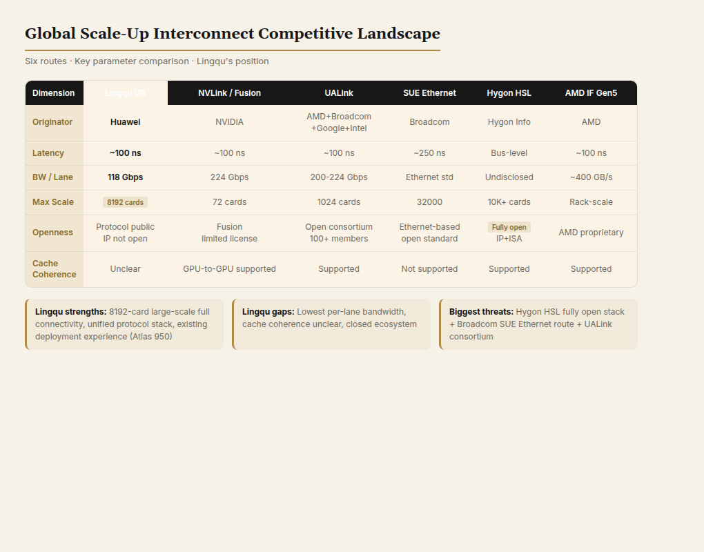
Here are the six main routes:
| Dimension | Lingqu (UB) | NVLink/NVLink Fusion | UALink | SUE (Scale-Up Ethernet) | Hygon HSL | AMD IF Gen5 |
|---|---|---|---|---|---|---|
| Initiator | Huawei | NVIDIA | AMD+Broadcom+Google+Intel+Meta, etc. | Broadcom | Hygon | AMD |
| Latency | ~100 ns | ~100 ns | ~100 ns | Sub-microsecond (~250ns) | Bus-level (exact value undisclosed) | ~100 ns |
| Bandwidth/Lane | 118 Gbps | 224 Gbps (NVLink 6) | 200-224 Gbps | Ethernet standard rates | Undisclosed | ~400 GB/s die-to-die |
| Max Scale | 8,192 cards | 72 cards (NVL72) | 1,024 cards | 32,000 GPUs | 10,000+ cards | Rack-level (Helios) |
| Openness | Protocol public, hardware IP not open | Fusion limited licensing | Open consortium standard | Based on Ethernet | Full-stack open (IP + instruction set) | AMD proprietary |
| Ecosystem Maturity | Low (Huawei ecosystem) | High (CUDA) | Medium (100+ members) | High (Ethernet) | Low (just starting) | Medium (AMD ecosystem) |
| Cache Coherence | Not specified | Supported between GPUs | Supported | Not supported | Supported (IF heritage) | Supported |
Several key observations:
-
Lingqu trails NVLink 6 and UALink in bandwidth per lane (118 Gbps vs. 224 Gbps), but its advantage lies in large-scale full mesh. NVLink 5 tops out at 72 cards; Lingqu can reach 8,192.
-
UALink is Lingqu's direct competitor on the global stage. Both target "bus-level unified interconnect," but UALink takes the open consortium route, backed by heavyweights like AMD, Broadcom, Google, and Intel. Lingqu takes the "Huawei self-developed + protocol published" route. More importantly, UALink inherits five generations of IF's cache coherence and memory semantics engineering experience — a shortcoming Lingqu hasn't yet addressed.
-
Hygon HSL is Lingqu's most important competitor in the domestic market. HSL's technology comes from IF licensing, giving it a high starting point. And Hygon chose a full-stack open strategy (IP + instruction set + reference design), which is more attractive than Lingqu's "protocol public but hardware IP not open." HSL's weakness is its nascent ecosystem, but Hygon's "open interconnect provider" positioning is inherently more acceptable to other domestic chipmakers than Huawei's "full-stack self-development."
-
AMD IF Gen5 (Helios) is a variable worth watching. AMD uses IF Gen5 to interconnect CPUs, GPUs, and DPUs within a single rack, while supporting both UALink and Ultra Ethernet for external scaling. This is AMD's "unified internal interconnect + open external interface" strategy. If AMD's Helios platform successfully ships in H2 2026, it will demonstrate that a UALink + Ethernet dual-layer architecture can deliver sufficient performance — posing a direct challenge to Lingqu's "unified protocol stack flattening all layers" approach.
-
Broadcom's SUE (Scale-Up Ethernet) is an underestimated variable. Broadcom chose not to build a dedicated bus protocol, instead using Ethernet for Scale-Up interconnect. Tomahawk Ultra delivers 250ns latency and 51.2 Tbps capacity, with trimmed headers and CBFC flow control — approaching bus-level performance in MoE inference scenarios. This route's openness and cost advantages may be more appealing than UALink.
6. Protocol Stack Layer-by-Layer Breakdown
The previous chapters addressed "what Lingqu is" and "why it's designed this way." This chapter digs into "how it actually works." The focus is on the physical layer — where Huawei's engineering capabilities are most concentrated, where public information is scarcest, and where the work is most easily underestimated.
6.1 Physical Layer
The physical layer is the foundation of the Lingqu protocol stack and the most concentrated expression of Huawei's engineering capabilities. According to technical details from the Lingqu Protocol Decoding public course, the physical layer contains three sub-modules: PCS (Physical Coding Sublayer), PMA (Physical Medium Attachment), and Link Management State Machine (LMSM).
Dual-Mode Design: Mode-1 Custom + Mode-2 Compatible
Lingqu's physical layer provides two PHY modes — this is the key entry point for understanding Lingqu's design philosophy:
| Parameter | PHY Mode-1 | PHY Mode-2 |
|---|---|---|
| Data Rate | 4.0 Gbps + custom rates | 2.578 / 25.78 / 53.125 / 106.25 Gbps |
| Modulation | NRZ at 4.0 Gbps; NRZ or PAM4 for custom rates | NRZ at low speeds; PAM4 at 53.125/106.25 Gbps |
| Positioning | Custom rates, unconstrained by fixed standard rates | Compatible with IEEE 802.3-2022 / 802.3ck-2022 |
Mode-1's design intent is to fully leverage SerDes and channel capability, unconstrained by Ethernet's fixed speed tiers (25G/50G/100G/200G/400G). Ethernet's speed tiers are engineering compromises for backward compatibility — each generation must interoperate smoothly with the previous one. Lingqu doesn't need this compatibility baggage, so Mode-1 can push SerDes to the physical limits of the channel.
Mode-2 ensures Lingqu can reuse Ethernet's mature physical layer ecosystem (cables, connectors, optical modules), reducing deployment costs.
Data Path: Training Code Stream and Data Code Stream
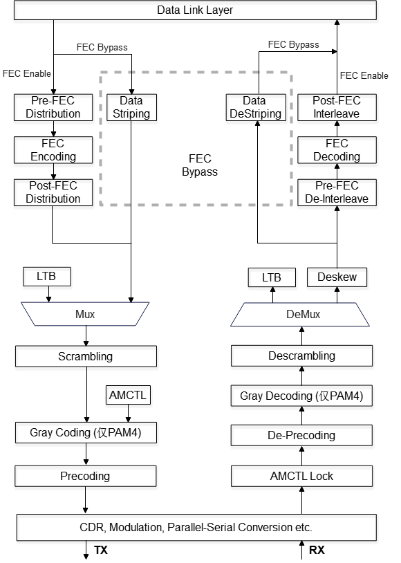
The physical layer's data path is split into two:
- Training Code Stream (link training state): Transceivers exchange link training codes (LTB), without FEC encoding/decoding. This is the initialization process bringing a link from unavailable to available.
- Data Code Stream (link available state): Includes FEC, scrambling, precoding, and Gray coding (for PAM4 modulation). FEC can be bypassed at low speeds or when link quality is excellent, reducing latency.
Both code streams periodically interleave AMCTL (management control words) for frame delineation and extended control functions. AMCTL uses eBCH-16 encoding (BCH(15,5) + 1 bit even parity), capable of correcting any error up to 3 bits and some 4-bit errors. AMCTL bypasses scrambling and isn't within FEC protection scope. Default insertion interval is 6,656 symbols.
The elegance of this design: AMCTL serves as the physical layer's "in-band control channel," maintaining link management capability even when the data code stream experiences errors.
FEC Design: Low Latency First
Lingqu's FEC supports multiple modes. Core parameters:
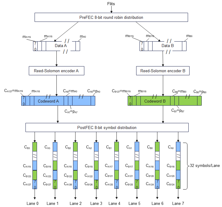
| FEC Mode | N | K | T | Interleaving Mode |
|---|---|---|---|---|
| RS(128,120,T=2) | 128 | 120 | 2 | 1-way or 2-way |
| RS(128,120,T=4) | 128 | 120 | 4 | - |
Key design choice: Lingqu's interleaving strategy is "symbol distribution" rather than traditional interleaving. Traditional interleaving shuffles symbols across multiple codewords — strong error correction but high latency. Lingqu only distributes symbols without interleaving, maintaining low latency. The small number of uncorrectable errors are handled by link-layer retransmission.
This choice reflects Lingqu's priority: in AI training and inference, latency matters more than extreme reliability. Occasional retransmission (nanosecond-scale) has less impact on throughput than sustained high FEC latency (hundreds of nanoseconds).
FEC also supports dynamic switching: FEC mode is adjusted in real-time based on link quality. Good link quality uses lightweight FEC (T=2), poor quality uses strong FEC (T=4), and FEC can even be bypassed entirely.
LMSM: The Engineering Depth of Link State Management
LMSM (Link Management State Machine) is one of the physical layer's core competencies. It handles link training and fault recovery, supporting:
- Electrical and optical links
- Link width negotiation and dynamic width switching
- Forced fast lane reduction on fault (microsecond-scale, without entering Retrain state)
- Fixed-rate mode and rate negotiation/switching mode (downshifting when BER is too high)
- FEC mode negotiation and dynamic switching
- Full lane reordering and lane polarity detection/flip
- Equalization negotiation
Dynamic lane scaling deserves its own analysis.
Traditional interconnects (like PCIe) require retraining the entire link when a lane fails — interrupting all data transmission for milliseconds. Lingqu's LMSM can complete lane reduction in microseconds: it doesn't enter the Retrain state, only disables the failed lane while other lanes continue transmitting. Combined with link-layer retransmission, there's zero packet loss during faults.
Going further, "dynamic link width switching" allows lanes to be scaled up or down during active operation based on traffic demand: fewer lanes when traffic is low (saving power), more lanes when demand peaks. This means Lingqu's physical layer isn't statically configured — it adaptively adjusts based on runtime conditions.
SerDes Unification: The Foundation of Lingqu's Unified Architecture
One easily overlooked but critically important design in Lingqu: all traffic types (bus, network) share the same set of SerDes.
In traditional architectures, PCIe SerDes and Ethernet SerDes are separate. An XPU that needs both bus and network interconnect requires two independent SerDes sets and controllers. Inter-node communication also requires conversion between these two SerDes types, adding area and latency.
Lingqu unifies SerDes through UB — the same SerDes can be used for all traffic types, with no conversion needed. This directly reduces chip area (no duplicate SerDes) and physical latency (no protocol conversion).
Lane Rate Positioning
Lingqu's 118 Gbps/Lane (Mode-1) sits between Ethernet's 106.25 Gbps (Mode-2 / 802.3ck) and NVLink/UALink's 224 Gbps. This rate choice is an engineering tradeoff:
- 11% faster than Ethernet, providing bandwidth advantages in bus-level interconnect
- Not chasing NVLink's 224 Gbps, reducing SerDes design difficulty and power consumption
- Combined with large-scale full mesh (8,192 cards), using parallel lane count to compensate for per-lane bandwidth differences
But to be honest: the per-lane bandwidth gap means Lingqu needs more lanes at equivalent interconnect domain scale, increasing pin usage and cable complexity. Within area- and power-constrained packages (like Chiplets), lane count is a hard constraint.
6.2 Link Layer
The link layer is based on Flit transmission:
- Flit: Minimum transmission unit, 20 bytes
- Block: 32 Flits (640 bytes)
- Packet: 1-16 Blocks (640 bytes - 10 KB)
The link layer provides CRC verification and optional link-layer retransmission. The retransmission mechanism is "remote detection, source retransmission." The receiver, upon detecting packet loss, requests retransmission from the sender rather than the sender blindly retransmitting. This is more efficient but requires the receiver to maintain additional reordering buffers.
6.3 Network Layer and Transport Layer
The network layer handles routing and forwarding, supporting multipath and virtual channels to avoid deadlocks.
The transport layer's design is a highlight of Lingqu: three modes chosen on demand.
| Mode | Overhead | Reliability | Use Case |
|---|---|---|---|
| UTP | Highest | Full reliable transport | Data transfers requiring strict guarantees |
| CTP | Medium | Streamlined reliable transport | Balancing performance and reliability |
| RTP | Lowest | No transport-layer guarantees | Latency-sensitive, tolerates minor packet loss |
| TP Bypass | Zero | No transport layer | Synchronous memory access with most extreme latency requirements |
Compared with NVLink and PCIe:
- NVLink has no transport-layer concept; hardware directly ensures reliability.
- PCIe has a complete transport layer (Transaction Layer + Data Link Layer) but can't bypass it.
- Lingqu's flexibility shows here: for the frequent small-message All-to-All communication in MoE inference, Bypass mode significantly reduces latency; for large-block model parameter transfers, UTP provides reliable guarantees.
6.4 Programming Model
Lingqu provides two memory access semantics:
Synchronous Semantics: Load/Store
- Compute units directly issue L/S instructions, accessing remote memory through the UB Controller
- Latency: ~100 nanoseconds
- Suitable for fine-grained, frequent memory access (e.g., gradient synchronization, parameter updates)
Asynchronous Semantics: URMA (Unified Remote Memory Access)
- Similar to RDMA, but integrated within the UB protocol stack — no separate RDMA NIC needed
- Supports 64B - 4KB variable-length single-transaction operations
- Suitable for large-block data transfers (e.g., All-Reduce, Broadcast)
Both semantics share the same multi-port bandwidth pool, utilizing physical bandwidth through multipath transmission.
7. What Third Parties Need to Change to Support Lingqu
With the technical analysis done, a natural question: assuming the Lingqu protocol is fully open, how much change would a GPU vendor or system vendor need to make to support UB?
The answer: it involves the full stack, from silicon to software. This chapter can serve as a checklist — you don't need to read every item closely, but you should feel the scale of the engineering effort.
7.1 Chip Level
GPU/NPU Chips
This is where the changes are largest. Current GPU/NPU chips' I/O interfaces are primarily PCIe Controllers (connecting to CPU) and proprietary high-speed interconnect interfaces (like NVLink, Infinity Fabric). Supporting Lingqu requires:
-
Integrating UB Controller IP: The UB Controller is the hardware implementation of the Lingqu protocol stack, including physical layer (PHY + SerDes), link layer, network layer, transport layer, and transaction layer logic. This isn't a simple PCIe Controller replacement. The UB protocol stack is far more complex than PCIe, supporting synchronous/asynchronous memory semantics, multipath routing, link-layer retransmission, and more.
-
Integrating UMMU Module: UMMU (UB Memory Management Unit) handles global address translation and access authentication. Every UBPU needs a UMMU to translate remote UBA (UB Address) to local physical addresses while performing permission checks. UMMU's design philosophy is similar to IOMMU but needs to support UB's unique EID + Token authentication model.
-
EID and Routing Table Assignment: Each UBPU needs a globally unique EID and routing tables distributed by UBFM. This requires dedicated configuration registers on the chip and a management interface to communicate with UBFM.
-
NoC Integration: The UB Controller needs to interface with the chip's internal NoC (Network-on-Chip). Compute units (AI Cores, Tensor Cores, etc.) access the UB Controller through the NoC to initiate Load/Store or URMA operations. The NoC design must account for UB's multi-port, multipath characteristics.
-
SerDes/PHY IP: If using PHY Mode-1 (118 Gbps/Lane), SerDes IP supporting Lingqu's specific frequency points is needed. The good news is that third-party IP vendors are already working on UB PHY compatibility. Niuxin Semiconductor has publicly announced completing UB PHY IP compatibility verification, and VeriSilicon provides Chiplet integration services. This means third-party chipmakers don't necessarily need to develop their own SerDes.
CPU Chips
CPU changes are more complex than GPU because the CPU needs to manage UB's page tables and address space in kernel mode:
-
I/O Die Integration of UB Protocol Stack: Huawei's own Kunpeng processors already integrate UB Controller in the I/O Die. Third-party CPU vendors would need to do the same.
-
Kernel Page Table Management Overhaul: The Linux kernel needs to support UB's UBA address space, mapping remote memory into process virtual address spaces. This requires modifying the kernel's page table management and memory management subsystems.
-
URMA Asynchronous Interface: CPUs need to support URMA asynchronous operations, which may require new instructions or microarchitecture changes.
DPU/NICs
The traditional RDMA NIC role would be replaced by the UB Controller. Since UB natively supports URMA asynchronous memory access, a separate RDMA protocol stack isn't needed. But DPUs still have value: offloading security, compression, storage, and other advanced functions.
7.2 Board and Motherboard Level
Motherboard Routing
Current motherboards use PCIe slots as standard I/O interfaces. Supporting UB requires:
- UB Ports Replacing or Coexisting with PCIe Slots: Each UB Port needs multi-lane SerDes channels. Routing density and signal integrity requirements far exceed PCIe. A motherboard carrying 64 NPUs needs hundreds of high-speed differential pairs; PCB layers might increase from the current 16-20 to 24-32.
- Optical-Electrical Hybrid Routing: Intra-rack uses direct cables (short distance); inter-rack uses optical modules (long distance). Motherboards need both electrical signal channels and optical module interface positions. OBO (On-Board Optics) solutions solder optical modules directly to the motherboard, shortening electrical signal paths but increasing assembly and rework difficulty.
- Power and Cooling: The UB Controller's own power consumption isn't negligible. Each UB Controller needs independent power. Combined with high-density SerDes power draw, motherboard power design needs a complete rethink. For cooling, the local heat density around UB Port areas may exceed even the GPU areas.
Rack Design
The Atlas 950 rack is designed around UB, not assembled from traditional GPU servers:
- Single rack: 64 NPUs + 4 CPUs + 1 standby board, with FullMesh cable connections inside the rack, no switches needed.
- 16 racks form an 8,192-card SuperNode, with single-tier UB Switch interconnect between racks.
- Liquid cooling is standard — high-density wiring plus high-power chips make air cooling impractical.
7.3 System Design Level
From "CPU-Centric" to "Peer-to-Peer Network"
Traditional server system design is CPU-centric: the CPU manages the PCIe bus, controls memory allocation, and coordinates all peripherals. If GPUs want to communicate, they either go through the CPU (via system memory as intermediary) or use private channels (NVLink) — both paths have limitations.
Lingqu architecture tears up the system design logic and starts over: all components are UBPUs with equal status, addressed via EIDs, communicating directly P2P. The CPU is no longer the traffic hub — it's a network node just like NPUs and DPUs.
This means:
-
The memory model changes. In traditional architecture, each server has its own local memory; cross-node access requires RDMA. Under Lingqu architecture, all UBPUs' memory forms a global address space (UBA). Any UBPU can directly access remote memory via Load/Store, just like accessing local memory. The UMMU hardware module handles address translation and permission checks, transparent to applications.
-
Boot and discovery mechanisms change. Traditional servers boot via BIOS → bootloader → OS. A Lingqu SuperNode's boot process requires UBFM to first discover all UBPUs, assign EIDs, and configure routing tables before nodes can begin operating. This is a distributed system boot problem — far more complex than single-machine boot.
-
The fault tolerance model changes. Traditional clusters rely on upper-layer software (e.g., checkpoint-restart) to handle node failures. Lingqu provides layered fault tolerance at the hardware and protocol level: physical-layer dynamic lane reduction, link-layer retransmission, network-layer rerouting. The goal is that when a single UBPU or link fails, the entire SuperNode recovers within microseconds, transparent to upper-layer applications. This target is aggressive; actual delivery needs large-scale deployment verification.
-
Resource scheduling changes. Traditional cluster schedulers allocate "machines" (CPU+GPU+memory bundles). A Lingqu SuperNode's scheduling unit can be finer-grained: UB Partition supports slicing NPUs, memory, and bandwidth among tenants at the hardware level, with microsecond-level dynamic adjustment. This provides hardware-level isolation for multi-tenant SuperNode sharing.
7.4 Software Level
Software adaptation is the other major engineering effort for Lingqu deployment.
Operating System
openEuler already integrates UB Service Core, providing Lingqu's complete software stack. But third-party OSes (Ubuntu, CentOS, Debian, etc.) need to adapt independently. Key changes:
- Kernel Memory Management: Supporting UBA address space, mapping remote memory into process virtual address spaces. This isn't simple mmap. UMMU needs to work with the kernel's page table management, handling page faults, TLB coherence, and more.
- Device Driver Model: Traditional Linux device model is based on PCIe bus (device/driver/bus three-layer). UBPUs aren't PCIe devices and need a new driver framework. openEuler's implementation abstracts UBPUs as a new bus type.
- NUMA Extension: Traditional NUMA topology describes CPU and memory affinity. Under Lingqu architecture, NPUs, DPUs, and SSUs are all NUMA nodes. Topology description and scheduling policies need extension.
Communication Libraries and Frameworks
Huawei open-sourced the openFuyao communication library (serving a role similar to NCCL), supporting Lingqu's native semantics. But mainstream AI frameworks (PyTorch, JAX, DeepSpeed) have their underlying communication built on NCCL or Gloo. Adapting to Lingqu means either rewriting the communication backend or building an NCCL compatibility layer on top of openFuyao.
The feasibility and performance cost of the compatibility layer are key questions. Huawei has already done some work: openFuyao provides NCCL-like API interfaces, lowering migration barriers. But the performance of collective communication operations like All-to-All and All-Reduce depends heavily on underlying hardware topology. Lingqu's FullMesh topology differs significantly from traditional Clos topologies, so communication algorithms need re-optimization.
Compiler
Lingqu's URMA asynchronous semantics and Load/Store synchronous semantics require compiler awareness. Specifically:
- Compilers need to know which data is local and which is remote, and choose synchronous or asynchronous semantics accordingly.
- For gradient synchronization in distributed training, compilers need to generate URMA operations rather than traditional MPI calls.
- Huawei has done this work in the BiSheng compiler, but third-party compiler (LLVM, GCC) adaptation hasn't shown public progress.
Judgment: The software adaptation workload is significant but easier to advance than hardware adaptation. The reason is that software adaptation can be phased — first building an NCCL compatibility layer to get mainstream frameworks running, then gradually optimizing to Lingqu's native semantics. Hardware adaptation has no such "just get it running" intermediate state.
8. NVLink Fusion: NVIDIA's Defensive Pivot
From this chapter onward, the analytical lens shifts from "what Lingqu is" to "what Lingqu is up against."
8.1 Why NVIDIA Is "Opening" NVLink
In June 2025, NVIDIA launched NVLink Fusion. To understand this move, you first need to understand how NVIDIA maintained its iron grip on the AI compute market through NVLink for so long.
NVLink isn't an isolated technology. It forms a tightly coupled system with CUDA, NVSwitch, the SHARP engine, and the NCCL communication library:
- CUDA's Unified Memory relies on NVLink for transparent cross-GPU memory access
- Tensor Parallelism depends on NVLink's low-latency All-to-All
- NCCL's All-Reduce implementation relies on NVSwitch's SHARP engine for in-network reduction
- CUDA's programming model assumes all GPUs live in a unified address space
This system means that once NVIDIA's customers adopt CUDA, leaving the NVLink ecosystem becomes extremely difficult. NVLink's closed nature isn't a side effect — it's a design goal.
NVLink Fusion breaks open a small part of this closed system, but only a small part. The core offering: allowing third-party chips (CPUs, DPUs, custom accelerators) to integrate NVLink interfaces and participate in NVLink interconnect domains.
8.2 NVLink Fusion's Design Constraints
NVLink Fusion's "openness" is carefully bounded:
Constraint One: GPUs are not open. Third-party chips can only be "leaf nodes" in the NVLink Domain — they can't be GPUs. You can't use NVLink Fusion to plug your own AI accelerator into an NVIDIA GPU cluster; you can only connect CPUs or DPUs. AI accelerator-to-accelerator interconnect still goes through NVLink exclusively, and NVLink only works between NVIDIA GPUs.
The logic of this constraint is clear: NVLink is the moat protecting NVIDIA's GPU market share. Opening GPU-to-GPU interconnect means filling in the moat. But opening CPU/DPU access expands the NVLink interconnect domain's reach, making NVIDIA's rack-level solution (NVL72) more complete.
Constraint Two: IP licensing required. NVLink Controller IP must be licensed from NVIDIA, with terms, pricing, and restrictions all determined by NVIDIA. This isn't an open standard — it's a licensing model. Getting a license means part of your chip design process must go through NVIDIA's review and cooperation.
Constraint Three: Scale ceiling unchanged. NVLink 5's interconnect domain ceiling is 72 GPUs (NVL72). NVLink Fusion adds CPU and DPU nodes, but the GPU count ceiling stays the same. NVIDIA's architecture roadmap shows Rubin Ultra NVL576 potentially pushing this to 576, but that's still NVLink 6's internal evolution — not something Fusion delivers.
8.3 Forward-Looking Analysis of NVLink Fusion
From a technical foresight perspective, NVLink Fusion exposes a structural problem NVIDIA faces: single-chip compute growth is slowing, interconnect domains need to expand, but NVLink's FullMesh topology makes engineering costs skyrocket at scale.
NVIDIA's solution is to layer NVSwitch on top of NVLink for switched interconnect. NVL72 uses one tier of NVSwitch; NVL576 might use two. Switched interconnect scales well, but every additional switch tier adds 100-200 nanoseconds of latency. For latency-extremely-sensitive scenarios like MoE inference, each extra switch tier means significant throughput loss.
NVLink Fusion's real value may not lie in "openness" but in letting NVIDIA's customers mix their own chips within the NVLink interconnect domain. AWS's Trainium4 is the first public case — AWS can place its self-developed Trainium chips alongside NVIDIA GPUs within the same NVLink interconnect domain. This means cloud providers can build "NVIDIA GPU + custom accelerator" hybrid clusters without being entirely dependent on NVIDIA.
Implications for Lingqu: NVLink Fusion demonstrates that "opening dedicated interconnect protocols" is an industry trend. Lingqu is walking the same path, but more aggressively. NVLink Fusion's restriction (GPUs not open) means vendors wanting to build their own AI accelerators still need solutions beyond NVLink. Both Lingqu and UALink are candidates.
9. UALink and SUE: Two Open Routes and Their Design Philosophies
Lingqu's international competition isn't just NVIDIA. There are two open interconnect routes with fundamentally different design philosophies.
9.1 UALink: From Infinity Fabric to Open Standard
In April 2025, the UALink Consortium released the 1.0 specification. In April 2026, the 2.0 specification followed, adding in-network compute, Chiplet specification, and manageability specification.
UALink's Technical DNA: Engineering Experience from Five Generations of IF
Understanding why UALink could quickly release 1.0 and 2.0 specifications requires seeing the technical accumulation behind it. AMD's Infinity Fabric has evolved through five generations (see Chapter 4), progressing from intra-CPU interconnect all the way to CPU+GPU+DPU system-level interconnect. UALink's core design team comes from AMD, and many key protocol designs directly inherit IF's engineering experience:
- Load/Store Memory Semantics: IF Gen3 already implemented GPU-to-GPU Load/Store direct connection in MI250. UALink standardizes this capability, letting any vendor's accelerators access remote memory using unified semantics.
- Cache Coherence: IF Gen4 implemented cache coherence for shared CPU-GPU memory in MI300. UALink's shared memory model is directly based on this experience. Lingqu currently has no explicit cache coherence support — this is a structural advantage for UALink.
- Chiplet Integration: IF has been solving Chiplet-to-Chiplet communication since Gen1. UALink 2.0's Chiplet specification supports UCIe 3.0, letting chipmakers integrate UALink interfaces at the Chiplet level — directly from AMD's Chiplet combat experience.
But UALink isn't an open version of IF. IF is AMD's proprietary protocol; UALink is a consortium standard. The relationship is similar to ARM's AMBA and UALink: the former is vendor-proprietary, the latter is an open standard, but the design DNA shows clear lineage.
UALink's Design Starting Point
UALink's core question: Can an open standard deliver NVLink-level interconnect capabilities?
NVLink's core capabilities are three:
- Bus-level low latency (~100 ns)
- Load/Store memory semantics (GPUs can directly read/write remote memory)
- Full mesh topology (non-blocking communication between all GPUs in a rack)
UALink 1.0's design responds to each of these:
- Latency: UALink Switch latency targets vary with port count — under 200ns at 128 lanes, under 300ns at 512 lanes. This latency range is in the same order of magnitude as NVSwitch.
- Memory Semantics: UALink specifically emphasizes itself as "the only memory-semantic solution purpose-built for Scale-Up AI." It supports Read, Write, and Atomic transactions, enabling direct cross-accelerator memory access. Protocol efficiency is claimed at 94%+.
- Scale: 1.0 supports 1,024 accelerators. 2.0's Chiplet specification supports UCIe 3.0 integration, meaning UALink interfaces can be built into SoCs at the Chiplet level.
UALink 2.0's Forward-Looking Features
The 2.0 specification added several key capabilities:
-
In-Network Compute: Executing collective communication operations (like All-Reduce) within switches, similar to NVIDIA's SHARP. This reduces endpoint CPU overhead and network bandwidth consumption.
-
Link Resiliency: Automatic rate reduction or rerouting on link failure, without manual intervention. This is a hard requirement for large-scale deployment.
-
Link Folding: Multiple low-speed links aggregated into a single logical high-speed link. This lets systems flexibly combine physical layers of different speeds.
-
Manageability Specification: Introduces centralized management architecture using standard protocols like gNMI, YANG, SAI, and Redfish. This means UALink networks can be directly managed by existing network management tools.
-
Security Module (UALinkSec): Hardware-level encryption and authentication, supporting AMD SEV, Arm CCA, Intel TDX, and other trusted execution environments. This is critical for cloud provider multi-tenant scenarios.
UALink vs. Lingqu: Design Philosophy Differences
The two have nearly identical positioning but different design philosophies:
| Dimension | UALink | Lingqu |
|---|---|---|
| DNA | Infinity Fabric evolution | Brand-new self-development |
| Physical Layer | Based on Ethernet PHY (200GBASE-KR1/CR1) | Custom PHY Mode-1 + compatible Ethernet PHY Mode-2 |
| Lane Rate | 200-224 Gbps | 118 Gbps |
| Max Scale | 1,024 accelerators (1.0), expandable | 8,192 UBPUs |
| Openness | Consortium standard, 100+ members | Huawei self-developed, protocol public, hardware IP not open |
| In-Network Compute | Supported in 2.0 | No public information |
| Chiplet Integration | UCIe 3.0 compatible | No public information |
UALink's advantages lie in lane rate (200 Gbps vs. 118 Gbps) and ecosystem starting point (100+ consortium members vs. Huawei alone). Lingqu's advantages lie in networking scale (8,192 vs. 1,024) and actual deployment experience (Atlas 950 is in mass production).
But UALink has one structural advantage Lingqu lacks: its physical layer is based on Ethernet. This means UALink can reuse Ethernet's mature SerDes IP, optical modules, and cabling ecosystem. Chipmakers don't need custom PHY IP for UALink — they just implement the UALink protocol stack on top of the Ethernet physical layer. This dramatically lowers the barrier for third-party adaptation.
UALink's Risk: Misaligned interests within the consortium. AMD wants to push the Infinity Fabric evolution path, Broadcom wants to sell switch chips, Google and Meta want to reduce NVIDIA dependence, Intel wants to ensure its accelerators aren't marginalized. UALink 2.0 released four specifications at once — progress isn't slow — but whether a "the enemy of my enemy is my friend" alliance can sustain efficient collaboration remains the biggest uncertainty.
9.2 Broadcom SUE: Using Ethernet to Eat Scale-Up
Broadcom chose not to build a new protocol. Instead, it uses Ethernet for Scale-Up interconnect. The design philosophy: don't chase peak performance; use ecosystem maturity and cost advantages to cover 80% of scenarios.
Tomahawk Ultra's Design Approach
In July 2025, Broadcom launched Tomahawk Ultra, a 51.2 Tbps switch ASIC purpose-built for Scale-Up Ethernet. It's not just an Ethernet switch — it's deeply customized for AI workloads:
- Full line-rate at 64-byte packets: Traditional Ethernet switches optimize for large-packet throughput; small-packet performance degrades severely. Tomahawk Ultra delivers full 51.2 Tbps even at 64-byte packets, with latency under 250 nanoseconds. This is critical for the high-frequency small-message All-to-All communication in MoE inference.
- Trimmed Headers: Reduces Ethernet packet headers from 46 bytes to 10 bytes, dramatically improving small-packet payload ratios.
- Link-Layer Reliable Transport (LLR) + FEC: Completes error recovery at the link layer, avoiding upper-layer retransmission. Combined with credit-based flow control (CBFC), builds a near-lossless switching fabric.
- In-Network Collective (INC): In-switch reduction for All-Reduce and other collective operations, similar to NVIDIA's SHARP.
These optimizations brought Ethernet's Scale-Up latency from the traditional microsecond range down to sub-microsecond. While still 3-5× slower than NVLink/UALink's ~100 ns, it's "good enough" for many scenarios.
Tomahawk 6's Forward-Looking Design
Tomahawk 6, which entered mass production in June 2025, is even more aggressive: single-chip 102.4 Tbps switching capacity, 512 200G SerDes lanes, 3nm + Chiplet process. It simultaneously supports both Scale-Up and Scale-Out, meaning one chip can handle both intra-rack and cross-rack communication.
Tomahawk 6's key design choices:
- Unified Scale-Up/Scale-Out: No longer needs different switch chips for intra-rack and cross-rack communication. One chip serves both purposes, reducing system complexity and cost.
- Native CPO (Co-Packaged Optics): Optical engines and switch ASIC packaged on the same substrate, with signal transmission paths shortened to under 2 cm. This dramatically reduces power and latency — a key technology for large-scale AI cluster deployment.
- 1M+ XPU Cluster Support: Adaptive routing algorithms and large-scale topology support, targeting future million-accelerator clusters.
What SUE Means for Lingqu
Recall the InfiniBand vs. Ethernet history: InfiniBand was superior in both latency and bandwidth, but Ethernet leveraged cost and ecosystem advantages to push InfiniBand into an HPC niche.
The same story could repeat in Scale-Up interconnect. If Ethernet can deliver "80% of the performance at 50% of the cost with 10× the ecosystem maturity," most vendors will choose Ethernet. Tomahawk Ultra's 250ns latency may be slower than Lingqu's ~100 ns, but the gap is modest for most training tasks. The real differentiator is high-frequency small-message All-to-All in MoE inference — and Broadcom is closing that gap with trimmed headers, CBFC, and other techniques.
Lingqu's real competitor may not be UALink but SUE. The UALink consortium's execution is uncertain, but Broadcom is a company with proven execution, and the Ethernet ecosystem has been running for decades. If Broadcom makes Ethernet Scale-Up practically viable by 2027-2028, Lingqu's time window will narrow dramatically.
10. Ecosystem Adoption: Who Will Use Lingqu
The technical and competitive analysis is done. The final question, and the most practical one: besides Huawei itself, who will use it?
Certainty Within the Huawei Ecosystem
Lingqu's adoption within the Huawei ecosystem is certain:
- Ascend + Kunpeng: UB Controller already integrated, full stack connected from chips to systems to software.
- Atlas Product Line: Atlas 300 (inference card), Atlas 500 (edge), Atlas 800 (training server), Atlas 900/950 (SuperNodes) — all support or plan to support Lingqu.
- Huawei Cloud: ModelArts platform's training clusters already use Lingqu interconnect at the infrastructure level.
- openEuler + openFuyao: Open-source software stack, lowering customer adaptation barriers.
This installed base isn't small. Huawei's domestic AI compute market share has exceeded 60%, and domestic procurement in government, finance, energy, and telecom is essentially guaranteed incremental growth.
Third-Party Chipmaker Decisions
This is the key to whether Lingqu can break out of the "Huawei ecosystem." Third-party AI accelerator vendors (Biren, SweiYuan, MetaX, Tianshu Zhixin, etc.) face a choice:
Option A: Join the Lingqu Ecosystem
- Advantage: Direct access to Huawei's Atlas SuperNode system, gaining deployment opportunities through Huawei Cloud and Huawei's channels. In the domestic government and enterprise market, this path has strong commercial logic.
- Cost: Core interconnect IP depends on Huawei (UB Controller, UBFM), limiting chip design autonomy. And adapting the UB protocol stack requires significant engineering resources — a non-trivial cost for cash-strapped startups.
Option B: Take the Ethernet Optimization Route
- Advantage: Leverage the Ethernet ecosystem, low adaptation cost, no dependence on a single supplier. If UEC standards mature in the future, seamless upgrades are possible.
- Cost: Performance ceiling constrained by Ethernet latency. May fall short of Lingqu in large-scale MoE inference scenarios.
Option C: Wait for UALink's Chinese Version (OISA)
- Advantage: If OISA standards materialize, it would provide UALink-like open interconnect capabilities while maintaining domestic autonomy.
- Cost: OISA is currently in the standards discussion phase with uncertain timelines. Waiting means potentially missing the 2026-2027 domestic compute procurement window.
Realistic Judgment: In the near term (2026-2027), Option B is the most pragmatic choice for most domestic AI chip vendors. The reason isn't that Ethernet is technically superior, but that it's "good enough, no strings attached, no bets required": a mature supply chain, the largest talent pool, and iteration that follows the UEC standard. Only when customers explicitly demand 10,000+ card full-mesh do Lingqu (Option A) or HSL enter consideration. Option A's channel advantage is real, but for chip vendors, channels are rented while interconnect IP is locked in — going with Option A for a specific project is understandable short-term, but strategically, not tying yourself to a single supplier preserves long-term optionality.
Cloud Provider Choices
Domestic cloud providers' attitudes are more nuanced:
- Alibaba Cloud: Has its own EthLink/Eth-X route, unlikely to fully embrace Lingqu. But Alibaba Cloud also sells Ascend instances, so limited Lingqu support is possible.
- Tencent Cloud: No self-developed interconnect protocol, but no public endorsement of Lingqu either. More likely to take the Ethernet route.
- Baidu Smart Cloud: Has self-developed Kunlun chips; has explicitly chosen the Ethernet route for interconnect. The Tianchi 256-card SuperNode (launching June 2026) uses custom high-bandwidth switches, not Lingqu. Baidu's choice further validates Ethernet's appeal to third-party vendors.
- ByteDance: Self-developed ZCube architecture takes the Ethernet route, explicitly not using Lingqu.
Cloud providers' core concern is avoiding single-supplier lock-in. Lingqu's closed nature (core IP from Huawei) makes cloud providers naturally wary.
Domestic GPU Interconnect Standards: Who Will Win?
This brings us to a more fundamental question: in the domestic GPU interconnect space, who will ultimately emerge? Do latecomers still have a chance? Should GPU vendors develop their own interconnect technology? Can independent interconnect-focused companies survive?
The landscape. There are currently four types of players:
- Huawei Lingqu — self-developed bus protocol, tied to Ascend ecosystem, IP fully proprietary
- Hygon HSL — Infinity Fabric licensing route, moving toward openness, relatively clean role
- Ethernet route — Alibaba EthLink, Baidu Tianchi, leveraging the UEC ecosystem
- OISA — still in standards discussion, timeline uncertain
Who will win? It depends on which market.
In the government/enterprise and domestic procurement market, Lingqu will likely be the de facto standard. Customers in this market don't need to choose — they buy Huawei Atlas cabinets, and Lingqu comes standard. Huawei's channel advantage here is nearly insurmountable. HSL can capture a slice (Hygon's own customers plus enterprises wary of Huawei lock-in), but unlikely to shake Lingqu's base.
In the internet and commercial market, Ethernet will likely dominate. Baidu Tianchi and Alibaba EthLink have already voted with real money. These customers have in-house capability and don't need anyone to "authorize" an interconnect protocol — they need high-performance switches and good scheduling software. The Ethernet ecosystem naturally meets this need.
So the real question: will China converge on a single interconnect standard?
Most likely not. The domestic AI compute market will fragment like the global market — Huawei camp uses Lingqu, AMD camp uses HSL, internet camp uses Ethernet. The only variable: if someday domestic GPUs truly need cross-vendor interconnection (e.g., heterogeneous cluster mixed scheduling), who can provide a cross-vendor interconnect abstraction layer? That position is currently vacant — and represents the biggest opportunity window.
Should GPU vendors develop their own interconnect technology?
In most cases, no.
Interconnect protocol development has an extremely high barrier — SerDes PHY, FEC encoding/decoding, link training state machines, large-scale routing algorithms. Each layer requires years of engineering accumulation. For most GPU vendors, resources spent on interconnect R&D would yield far more if invested in compute cores and software stacks.
The right strategy: pick an existing route to plug into, and concentrate engineering resources on differentiation. Cambricon chose to integrate with Lingqu; Biren chose CUDA compatibility with PCIe+Ethernet. Both are pragmatic. Self-developed interconnect only makes sense when your chip volume is large enough that custom interconnect is needed to extract performance — roughly 100,000+ units shipped annually.
Can independent interconnect-focused companies survive?
Yes, but the window is narrow and the business model needs careful thought.
Globally, not many interconnect-only companies thrive. Broadcom's switch ASIC + SUE route is competitive because Broadcom is already a switching giant — SUE is an extension of its capabilities, not a startup direction from scratch.
Domestic independent interconnect vendors (like Niuxin Semiconductor providing PHY IP, and VeriSilicon providing Chiplet integration) have a more realistic positioning: be IP suppliers, not standard-setters. License UB/HSL/Ethernet PHY IP and controller IP to multiple GPU vendors, earning licensing fees and royalties. This business model works, but the ceiling is clear — the interconnect IP market is much smaller than the GPU market itself.
The truly imaginative path: become the provider of a cross-vendor interconnect abstraction layer. Not a new protocol, but a software + firmware suite that enables interoperability between Lingqu, HSL, and Ethernet. This requires understanding both bus protocols and Ethernet, handling protocol conversion and routing optimization — extremely difficult. But if someone pulls it off, it becomes the cornerstone of domestic AI compute interconnection, with value far exceeding single-protocol IP licensing.
Frankly though, this direction currently lacks clear commercial validation. Someone needs to build it first, then find customers willing to pay.
11. Core Judgments
Ten chapters of technical analysis done. Time to crystallize the judgments. Five points, ordered by importance.
Judgment One: Lingqu Is the Linchpin of Huawei's "Interconnect Compensates for Compute" Strategy
Huawei's AI compute strategy has a core logic: "using math to compensate for physics, non-Moore to supplement Moore." Single chips can't beat NVIDIA due to process restrictions, so use interconnect advantages to glue more chips together and win on system-level throughput. Lingqu is the infrastructure of this strategy. If Lingqu fails — if large-scale networking proves unreliable, latency falls short of expectations, or third-party chipmakers refuse to adopt it — Huawei's entire SuperNode strategy will be undermined.
Judgment Two: Lingqu's Competitive Window Is 2026-2027 — Shorter Than Expected
2026-2027 is Lingqu's critical window. Reasons:
- UALink 2.0 is released; actual products will ship at scale in H2 2027, faster than expected.
- AMD's Helios platform delivers in H2 2026, demonstrating that UALink + Ethernet dual-layer architecture works.
- Hygon HSL 1.0 is released; while the ecosystem is nascent, Hygon's full-stack open strategy is attracting domestic chipmakers.
- Broadcom Tomahawk Ultra is already in mass production; Ethernet Scale-Up performance is rapidly approaching bus-level.
Lingqu's time window isn't three years — it may be only 1.5-2 years. If it can't establish clear ecosystem advantages by end of 2027, a three-way squeeze from HSL, UALink, and Ethernet will push Lingqu back into Huawei's internal ecosystem.
Judgment Three: Lingqu's Core Domestic Threat Is Hygon HSL's Openness Advantage
NVLink is a closed but dominant interconnect standard. All NVIDIA GPUs must use NVLink — there's no choice. Lingqu can't achieve this status because Huawei lacks NVIDIA's chip market dominance.
In the domestic market, Lingqu faces a more specific problem: Hygon HSL is doing what Lingqu can't — becoming the unified interconnect standard for domestic chips. HSL's advantage isn't superior technology (IF-licensed bandwidth may fall short of Lingqu's 118 Gbps) but a "clean role": Hygon doesn't compete with other GPU vendors in the core compute market. It provides interconnect protocols for other vendors to plug into — a positioning that's inherently more acceptable.
Lingqu's counter-strategy should be further openness: not just publishing protocol specifications, but opening UB Controller IP, providing free licensing, and establishing an independent technical committee. But this means Huawei would need to relinquish control over Lingqu — a difficult decision to make.
For third-party chipmakers, the preferred path is Ethernet, and this is not merely a technical judgment but a commercial one:
- Technically: Ethernet means zero supplier lock-in, a mature supply chain, and the largest talent pool. Iteration follows the UEC standard. Only when customers explicitly demand 10,000+ card full-mesh do Lingqu or HSL enter consideration. It's not that Ethernet is technically superior — it's that it's "good enough, no strings attached, no bets required."
- Commercially: Choosing an interconnect protocol is fundamentally choosing an ecosystem position. Lingqu means deep Huawei dependency (even UB Controller IP must come from Huawei). HSL means allying with Hygon. Ethernet means allying with no one. In a market where supply chain security is acutely sensitive, this choice is rarely a pure technical comparison — it's a composite of commercial trust and risk appetite. Baidu Tianchi and Alibaba EthLink both chose Ethernet not because they don't understand bus protocols' advantages, but because it's the most commercially predictable choice.
Judgment Four: Lingqu's Real Risk Isn't Technical
Technically, Lingqu's five-layer protocol stack design is solid. The 118 Gbps/Lane rate, while trailing NVLink 6, is engineering-sound. The 8,192-card non-blocking full-mesh networking capability is the largest among publicly known solutions.
But the risks Lingqu faces aren't technical:
- Domestic chipmakers' fear of dependency: Nobody wants to hand their core interconnect to a company that's both supplier and competitor. Huawei is both the maker of Ascend chips and the controller of Lingqu's core IP. This dual role makes third parties hesitate.
- Commercial trust is harder to solve than technical specs: Third-party vendors choosing an interconnect protocol aren't just comparing bandwidth and latency. They're evaluating: if we choose Lingqu, will Huawei differentiate interfaces in three years? Will firmware updates prioritize Ascend? Will supply chain security audits flag us as "deeply dependent on Huawei"? These concerns can't be dispelled by technical documentation.
- Standards power dynamics: Lingqu is Huawei's self-developed protocol, not an open standard. Even with published specifications, core patents and hardware IP remain in Huawei's hands. The existence of open standards like OISA and UALink will continuously apply "not open enough" pressure on Lingqu.
- Non-technical constraints from export controls: Lingqu's SerDes speed and large-scale networking capabilities may touch sensitive export control lines. If the international environment tightens further, Lingqu's overseas expansion may be blocked.
Judgment Five: Lingqu's Greatest Commercial Value Is in Inference, Not Training
This judgment may be counterintuitive — most people assume large-scale training is where Lingqu shines most. But think carefully:
- Training's interconnect demand is bursty — it needs high-bandwidth All-Reduce during gradient synchronization but has low communication density at other times.
- MoE inference's interconnect demand is sustained — every inference triggers All-to-All communication (expert routing), extremely sensitive to latency. ~100 ns-level Load/Store direct memory access provides far greater throughput improvement for MoE inference than for training.
- As inference compute demand surpasses training (an industry trend), Lingqu's value in inference scenarios will keep growing.
DeepSeek V4-Pro's stable training on a 1,000-card Ascend cluster (MFU 34.9%) already proved Lingqu's viability for training. But Lingqu's greater commercial value may lie in MoE inference. Particularly under PD disaggregation architecture, the frequent KV Cache transfers between Prefill and Decode stages can benefit from Lingqu's unified memory semantics providing lower latency than RDMA.
12. Conclusion
Back to the title: Lingqu is the interconnect bet behind China's AI compute breakout.
Huawei is betting that in the AI compute era, interconnect matters more than single chips, and that a unified protocol stack spanning from physical layer to transaction layer beats stitching together existing protocols. This bet has merit. The proliferation of MoE architectures has indeed made interconnect the bottleneck — "faster, bigger GPUs" alone isn't enough anymore.
But whether the bet pays off doesn't depend entirely on technology. Lingqu needs to answer three questions:
- Will third parties follow? An interconnect protocol without an ecosystem is just a private solution. Lingqu needs to prove it's more than Huawei's internal tool.
- Is the time window wide enough? During the 2026-2028 window, Lingqu needs to scale from 8,192 cards to even larger sizes (Huawei has hinted at 100,000-card-level plans) while hardening reliability to production grade.
- How will openness be handled? Publishing protocol specifications is the first step, but it's not enough. The UB Controller IP licensing model, UBFM firmware openness level, and openFuyao's community governance structure — these are the indicators that will determine how "open" Lingqu truly is.
Huawei says "using math to compensate for physics." Lingqu is that math. But whether math can close the process gap ultimately depends on how many people are willing to use it.