
NVIDIA Rubin Respin: Is AMD's GPU Competitive Strength Worth the Hype?
A Taiwan Fubon research report reveals: Rubin's first version has taped out, but was pushed back for a redo due to MI450 competitive pressure. What did NVIDIA get right, and what did it get wrong? Why has AMD finally caught up to NVIDIA's rearview mirror?
1. A Chip Already in Fab, Pulled Back for a Redo
In August 2025, the Taiwan Fubon Financial Holdings research team published a report that sent shockwaves through the semiconductor industry. The core message came down to two sentences:
"Rubin's first version taped out at the end of June, but NVIDIA is redesigning the chip to better compete with AMD's upcoming MI450."
"We expect the next tape-out timeline to be late September or October. At that schedule, Rubin's 2026 shipment volume will be very limited."
Chip tape-out is one of the most expensive milestones in semiconductor product development. Mask costs at advanced nodes routinely run into tens of millions of dollars. Pulling back a chip that has already taped out and is running on TSMC's production lines means the previous mask money is wasted, and mass production is delayed by at least a quarter.
This doesn't happen often in the industry, but it's not unprecedented. The key question isn't whether NVIDIA has the ability to respin — it's what forced it to do so.
What Does NVIDIA Say?
NVIDIA's official response is the standard "everything is on track" — Rubin will still launch in 2026, and the annual cadence remains unchanged. CFO Colette Kress previously confirmed that the Rubin GPU and Vera CPU have been submitted to TSMC for production.
But the semiconductor industry has an unwritten rule: no company admits to a project delay unless the delay is impossible to hide. Fubon's report comes from first-hand supply chain information in Taiwan, giving it high credibility.
The Cadence Clue
Another piece of circumstantial evidence comes from EDA vendor Cadence. EE Times Europe reported that NVIDIA is using Cadence's power analysis tools to redesign Rubin. If you're just making minor tweaks, you don't need to bring in a new power analysis toolchain. This suggests the respin is substantial, at minimum involving a re-layout at the power optimization level.
Why Now?
Timing is critical. NVIDIA revealed Rubin's detailed specs at CES 2026 (January) and GTC 2026 (March). Meanwhile, AMD showed its MI400 series hand at its late-2025 Financial Analyst Day. When NVIDIA's engineers saw AMD's spec sheet, they likely realized one thing: if Rubin shipped as originally planned, it would fall behind AMD on several key dimensions.
Hence the respin.
2. What Pressure Did MI450 Actually Put on NVIDIA?
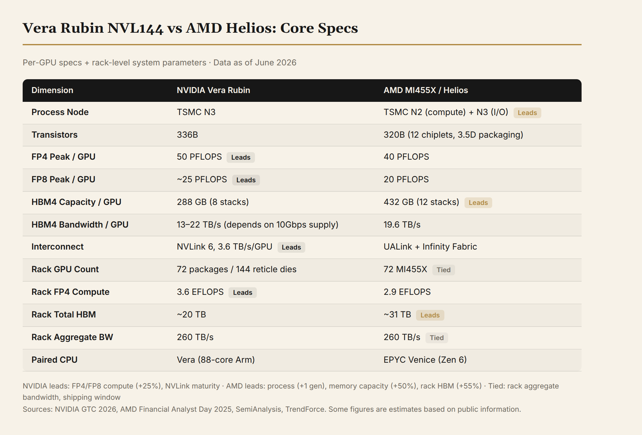
Let's look at the data.
| Dimension | NVIDIA Rubin (VR200) | AMD MI455X | Leader |
|---|---|---|---|
| Process | TSMC N3 | TSMC N2 + N3 chiplet hybrid | AMD |
| Transistor Count | 336B | 320B | Roughly even |
| Die Architecture | Dual reticle die monolithic integration | 12 chiplets (N2 compute + N3 I/O), 3.5D packaging | Different approaches, trade-offs on both sides |
| FP4 Peak Compute | 50 PFLOPS | 40 PFLOPS | NVIDIA +25% |
| FP8 Peak Compute | ~25 PFLOPS (estimated) | 20 PFLOPS | NVIDIA +25% |
| HBM4 Capacity | 288 GB (8 stacks × 12-Hi) | 432 GB (12 stacks × 12-Hi) | AMD +50% |
| HBM4 Bandwidth | 13–22 TB/s (depends on 10Gbps die availability) | 19.6 TB/s (12 stacks) | AMD baseline stronger; NVIDIA is betting on supply |
| Inter-GPU Interconnect | NVLink 6, 3.6 TB/s/GPU | UALink + Infinity Fabric | NVIDIA ecosystem maturity dominant |
| Rack Scale | NVL144: 72 packages / 144 reticle dies | Helios: 72 MI455X | Effective GPU count is the same |
| Rack Total Compute | 3.6 EFLOPS FP4 | 2.9 EFLOPS FP4 | NVIDIA +24% |
| Rack Aggregate Bandwidth | 260 TB/s | 260 TB/s | Tied |
| Rack Total HBM | ~20 TB | ~31 TB | AMD +55% |
| Paired CPU | Vera (88-core Arm) | EPYC Venice (Zen 6) | Each has advantages |
| Expected Ship Date | H2 2026 (volume may be limited) | H2 2026 | Time windows overlap |
Pressure Point 1: Process Node Overtake
This is what makes NVIDIA most uncomfortable. AMD's MI450 series will manufacture its compute chiplets on TSMC N2 (2nm-class) — the first time AMD has led NVIDIA on an AI GPU process node.
From the Maxwell era (2014) to now, NVIDIA has either led or matched on process node for data center GPUs. Even during the Hopper (H100, TSMC N4) and Blackwell (TSMC N4P) generations, AMD's MI300/MI350 used the same or older process. Now AMD hasn't just caught up — it has overtaken by a full node.
What does a process lead mean? At the same transistor budget, N2 delivers roughly 10-15% higher performance or 25-30% lower power consumption compared to N3. This gives AMD more thermal headroom in liquid-cooled racks — room to push clocks higher or pack in more compute units.
Pressure Point 2: Memory Capacity — 432 GB vs 288 GB
A 50% capacity advantage is not a rounding error. In frontier model training and inference, GPU memory directly determines tensor parallelism (TP) strategies — how you split model parameters across multiple GPUs for parallel computation.
Take a 1.8T-parameter MoE model: at 288 GB per GPU, you need at least 7-8 GPUs to hold all parameters; 432 GB drops that to 5. A lower TP degree means less interconnect communication overhead, higher compute utilization, and lower inference latency.
This also explains why NVIDIA is rushing to push suppliers for 10Gbps HBM4 in the respin — if bandwidth can go from 13 TB/s to 22 TB/s, NVIDIA could at least overtake AMD's 19.6 TB/s on the bandwidth dimension. But 10Gbps HBM4 is still in early mass production. Micron has confirmed sampling, but large-scale delivery is an open question. NVIDIA's respin is essentially a bet on the supply chain.
Pressure Point 3: A Real Rack-Scale Competitor Has Arrived
AMD's biggest shortcoming with MI300X/MI350X wasn't single-card compute — it was interconnect. SemiAnalysis put it bluntly: MI355X's scale-up domain (the group of GPUs sharing memory and cooperating on computation) is only 8 GPUs, while NVIDIA's GB200 NVL72 has 72. In large model inference and training, 72 GPUs working as a unified memory pool versus groups of 8 connected through a network — these are entirely different performance classes.
Helios changes this. 72 MI455X GPUs connect via UALink (Ultra Accelerator Link, an open-standard high-speed accelerator interconnect protocol) to form a rack-scale system with 260 TB/s aggregate bandwidth — matching NVIDIA's NVL144.
This is the first time AMD has delivered a rack-scale product on par with NVIDIA's.
Where NVIDIA Still Leads
To be fair, MI450's pressure isn't at the "performance crushing" level.
FP4 compute gap is significant. Rubin 50 PFLOPS vs MI455X 40 PFLOPS — NVIDIA leads by 25%. Given NVIDIA's Transformer Engine's deep optimization for low-precision inference, the real-world workload gap could be even larger.
Software ecosystem moat. CUDA's position won't be shaken in the near term. ROCm has improved substantially over the past two years (native PyTorch support, an increasingly mature HIP compatibility layer), but the maturity gap in large-scale production environments still exists. SemiAnalysis's 2025 benchmarks show that at identical hardware specs, CUDA's actual utilization (MFU) remains about 10 percentage points higher than ROCm's.
NVLink 6's track record. NVLink has been validated across multiple generations. UALink is a first-generation product. The stability and performance of a first-generation interconnect protocol in real deployments carries an open question mark.
The Nature of the Pressure
MI450's pressure on NVIDIA isn't "we beat you on a single card" pressure. It's "for the first time, simultaneously approaching or overtaking you on process, memory, and rack-scale" pressure.
When your competitor catches up or leads on several key metrics while your software and compute advantages are being steadily eroded, the rational strategy isn't to ship as planned — it's to spend a few months pulling the gap back open.
That's the logic of the respin.
3. AMD's AI Infra Chess Game
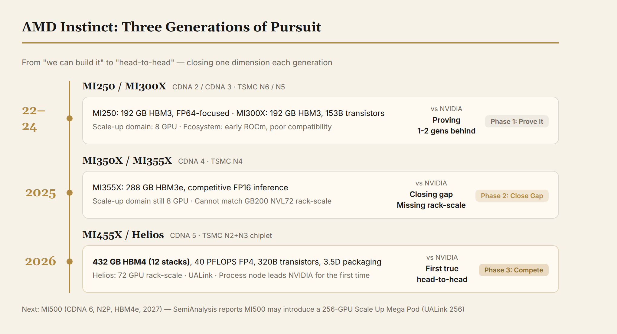
From MI250 to MI450: Three Generations of Catch-Up
AMD's catch-up trajectory in data center AI GPUs can be simplified into three phases:
MI250/MI300 (2022–2024): Proving it can build AI GPUs. MI250 used the CDNA 2 architecture to enter the AI training market for the first time, but performance and ecosystem both lagged NVIDIA by more than a generation. MI300X (CDNA 3) matched H100 on paper specs (192 GB HBM3 vs 80 GB HBM3), but ROCm's ecosystem gap kept many customers away.
MI350 (2025): Closing the gap. MI350X/MI355X (CDNA 4) became competitive on FP16/BF16 inference, but the rack-scale interconnect shortcoming (8-GPU scale-up domain) meant it couldn't challenge the GB200 NVL72 in frontier model scenarios.
MI400 (2026): First true head-to-head. MI455X (CDNA 5) doesn't just match or exceed Rubin on single-card specs (memory capacity) — it also, for the first time, has a 72-GPU rack-scale system (Helios). This is the first time AMD doesn't need to make excuses for "what NVIDIA has that I don't."
Investment Layout: From Chips to Full-Stack
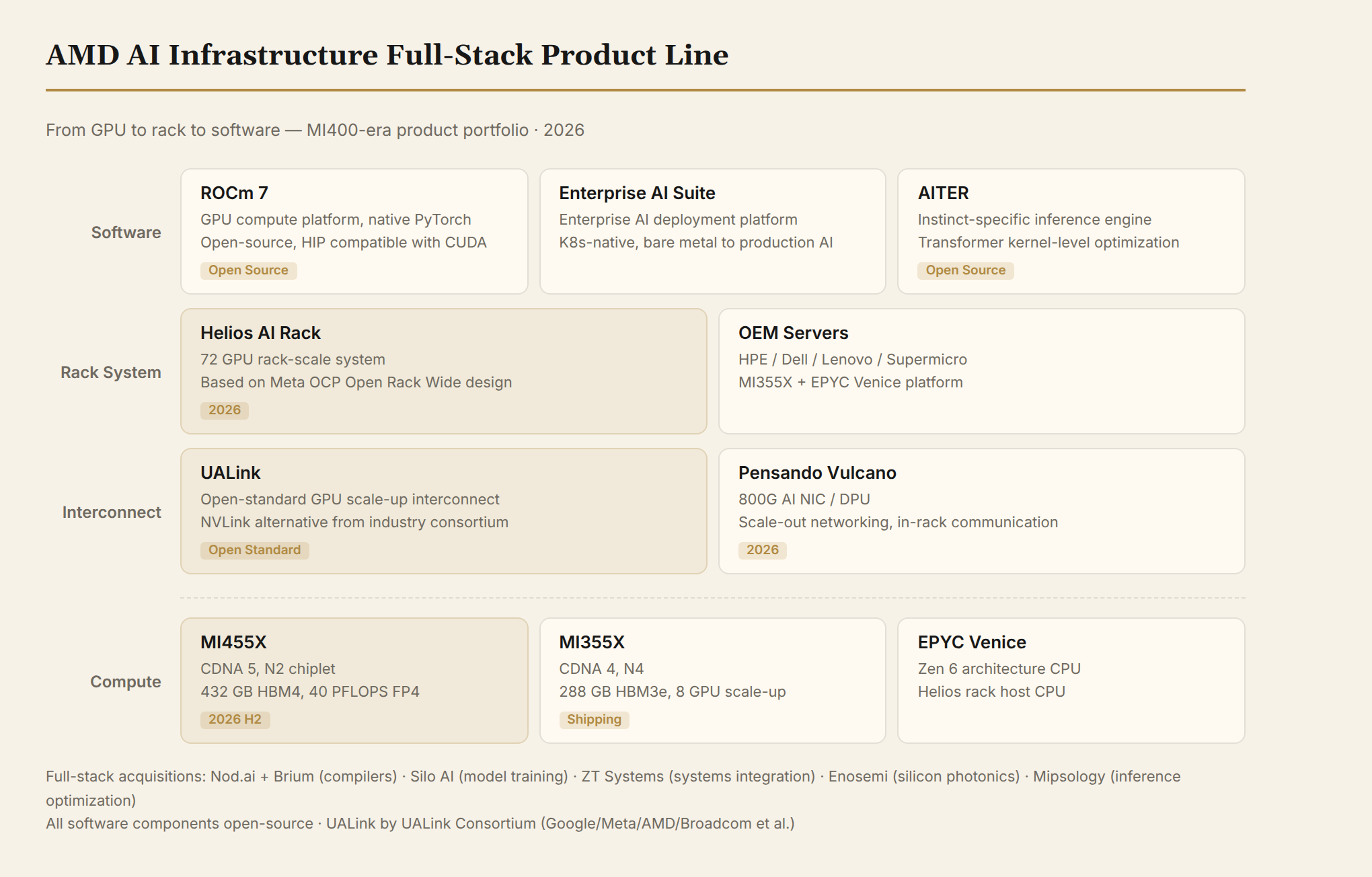
AMD has been on an intensive acquisition spree since 2023, targeting every weakness beyond the chip itself. Taken together, these acquisitions outline AMD's path from GPU vendor to AI infra full-stack supplier.
2023: Software layer foundation.
- Mipsology (undisclosed amount): French company focused on AI inference compilation optimization. Integrated into ROCm's inference optimization pipeline after acquisition — core technology enables models not optimized for AMD hardware to run faster on Instinct GPUs.
- Nod.ai (undisclosed amount): Open-source AI compiler company. Core product SHARK is an MLIR/IREE-based auto-compilation framework that compiles PyTorch/TensorFlow models to AMD GPUs automatically. Nod.ai makes "write once, run on AMD" much simpler.
2024: Model capability + systems integration.
- Silo AI ($665M): Europe's largest private AI lab, headquartered in Helsinki, Finland. Trained multiple open-source models on AMD platforms — Poro (Finnish LLM), Viking (Nordic languages LLM), and enterprise custom AI solutions. Continues operating as AMD Silo AI post-acquisition, serving as AMD's core engineering force for large model training and deployment, and AMD's beachhead in the European AI sovereignty narrative.
- ZT Systems ($4.9B): AMD's largest AI-related acquisition. ZT is a systems integrator that designs and manufactures custom AI server racks for hyperscale cloud vendors. Lisa Su put it plainly: "ZT lets AMD upgrade from providing chips to providing complete racks." AMD retained ZT's system design team (~1,000 engineers) post-acquisition and transferred manufacturing operations to Sanmina via a strategic partnership. The intent: when Meta or OpenAI says "I want 1GW of Helios racks," AMD can deliver directly.
2025: Continuing to fill gaps.
- Brium (undisclosed amount): Compiler and AI software optimization startup, focused on making AI software run efficiently on non-native hardware — essentially helping ROCm close the compiler-level gap with CUDA.
- Untether AI team (team acquisition): After this Canadian AI inference chip company ceased operations, AMD recruited its hardware and software engineering teams, gaining experience with at-memory architectures (computing near SRAM to reduce data movement).
- Enosemi (undisclosed amount): Silicon photonics startup using optical interconnects to replace electrical ones for higher GPU-to-GPU communication bandwidth and energy efficiency. This matters greatly for future rack-scale and pod-scale interconnect.
AMD has also taken strategic equity positions in multiple AI companies, investing over $125M in the past 12 months.
Product Planning: Not Just GPUs
AMD's AI infra product line now covers the full stack from CPU to networking:
| Component | Product | Role |
|---|---|---|
| GPU | MI300X → MI350X → MI355X → MI450 series | AI training and inference accelerators |
| CPU | EPYC Turin → EPYC Venice (Zen 6) | Rack-level CPU, paired with GPU |
| NIC/DPU | Pensando Vulcano (800G) | AI rack network smart card, handling scale-out communication |
| Rack System | Helios (ORW rack) | 72-GPU rack-scale system, based on Meta's Open Rack Wide design |
| Interconnect | UALink (open standard) | GPU scale-up interconnect |
| Software | ROCm 7 + AMD Enterprise AI Suite | Development tools, inference engine, deployment platform |
One notable detail: Helios's rack design is based on the Open Rack Wide specification Meta submitted to OCP (Open Compute Project). Meta is one of AMD's largest Instinct GPU customers, and Helios's design was tailored from the start for hyperscaler requirements and deployment habits.
Who's Using AMD GPUs?
Hyperscalers:
- Meta: The largest GPU procurement deal in industry history — multi-year, multi-generation, up to 6GW deployment. Initial 1GW based on custom MI450-architecture GPUs, shipping H2 2026. As part of the deal, AMD issued warrants to Meta, giving Meta the right to purchase up to 160M shares of AMD stock (~10% of outstanding shares). Meta's strategy is multi-vendor — the same week it signed a multi-year deal with NVIDIA.
- OpenAI: Another 6GW multi-year agreement, starting with MI450. OpenAI is also using AMD GPUs through a five-year cloud deal with Oracle (up to $300B).
- Oracle Cloud: First hyperscaler to publicly announce MI450 deployment. Initial 50,000 MI450 GPUs, starting Q3 2026. Also offering MI300X and MI355X instances.
- Microsoft Azure: One of the first cloud vendors to offer MI300X instances (ND MI300X v5 series, 1.5 TB HBM per VM), running its own open-source and proprietary model inference on MI300X on Azure. Has announced MI355X instance plans.
- Google Cloud: Deep EPYC usage on the CPU side; hasn't deployed Instinct GPUs at scale yet, but Google is a core member of the UALink Consortium.
Supercomputers / HPC:
- HPE El Capitan (Lawrence Livermore National Laboratory, USA): Based on MI300A APU (CPU+GPU integrated package). After going live in 2025, it was briefly the world's fastest supercomputer.
- LUMI (Finland, operated by CSC): Europe's largest GPU supercomputer, 11,900 MI250X GPUs, Top500 Europe #3. Widely used for large model training — AMD Silo AI's Poro and Viking models were trained on LUMI.
AI Cloud / Startups:
- TensorWave: North America's largest AMD-first AI cloud provider. Has deployed an 8,192 MI325X training cluster (per Tom's Hardware), and started offering MI355X instances. Clear positioning: AMD GPU compute for customers who don't want NVIDIA vendor lock-in.
- Neocloud ecosystem: dstack's 2025 Cloud GPU report shows growing numbers of neoclouds offering AMD MI300X/MI350X instances, typically priced 15-30% below comparable NVIDIA GPUs.
OEM ecosystem: HPE, Dell, Lenovo, and Supermicro have all announced MI355X-based server product lines. HPE is the first OEM partner for the Helios rack.
4. Hardware Architecture and Software Systems: The Deep Divergence Between Two Paths
Up to this point, we've discussed specs and ecosystem. But the deeper divergence between AMD and NVIDIA lies in chip architecture and software philosophy.
GPU Hardware Design: Chiplet vs Monolithic
The core architectural disagreement between AMD and NVIDIA is chiplet vs monolithic integration.
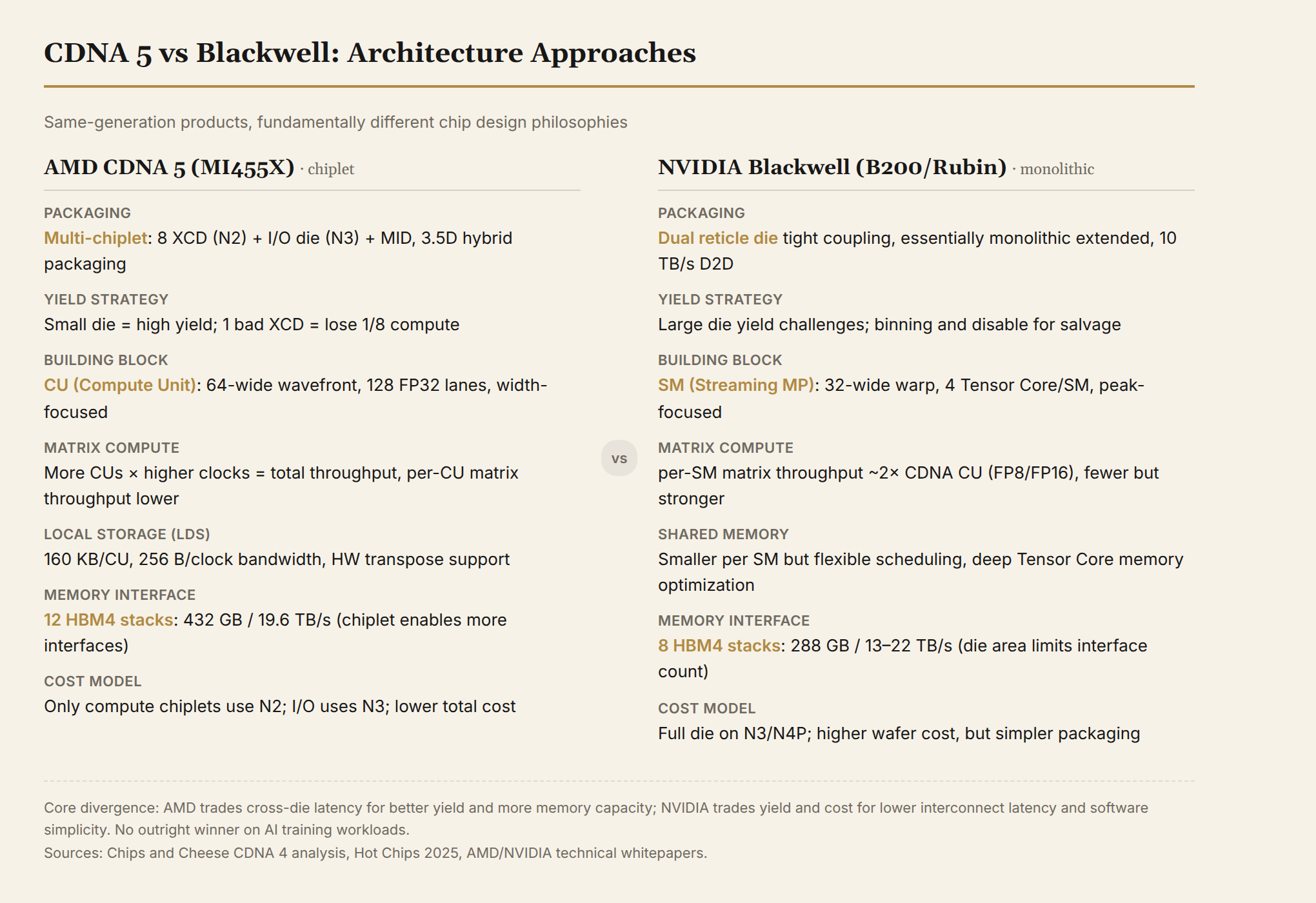
NVIDIA's path: Large monolithic dies. From Ampere (A100) to Hopper (H100) to Blackwell (B200), NVIDIA has consistently used the largest possible monolithic die. Blackwell made its first attempt at a dual-die design (two reticle-size dies connected via a 10 TB/s die-to-die interconnect), but this is fundamentally a tight coupling of two large dies — different from AMD's multi-chiplet disaggregation approach.
NVIDIA's reasons for monolithic:
- Lowest interconnect latency. Signal latency within a monolithic die is at the nanosecond level, while cross-die signals must traverse the packaging layer with higher latency and lower bandwidth. For an interconnect like NVLink that requires tight GPU-to-GPU coordination, low latency is a hard requirement.
- Simpler unified memory space. All compute units on a monolithic die share the same memory controller and L2 cache, eliminating complex cross-die cache coherency protocols. Software optimization is also simpler.
- Peak compute density. Ignoring yield constraints, a monolithic die can pack more compute units into a given area, typically delivering higher single-precision and low-precision peak compute.
AMD's path: Chiplet. AMD successfully transplanted this strategy from CPU (EPYC's CCD disaggregation) to GPU. MI300X's CDNA 3 architecture uses 8 XCDs (Accelerator Compute Dies) stacked on 4 base dies, each implementing 64 MB of Infinity Cache. MI355X's CDNA 4 inherits the same structure, slightly reducing CU count per XCD to improve yield. MI455X's CDNA 5 goes further — based on Linux kernel patches and Wccftech analysis, CDNA 5 may use 8 XCDs + multiple I/O dies + a dedicated Multimedia I/O Die (MID), integrated on dual interposers, totaling 32 billion transistors.
AMD's reasons for chiplet are equally solid:
- Yield. This is the most direct benefit. At advanced nodes (N2/N3), larger die areas cause yield to drop rapidly. The combined yield of 8 small dies is far higher than a single equivalently-sized large die. One failed N2 compute chiplet costs 1/8 of compute; one defective region on a large monolithic die scraps the entire GPU.
- Cost flexibility. Only compute chiplets use the most expensive N2; I/O dies and interposers use cheaper N3 or N6. N2 wafer prices are roughly 1.5-2× N3, so restricting N2 to compute cores significantly cuts total cost.
- Product derivatives. The same architecture can spawn multiple product SKUs by combining different numbers of chiplets. MI455X uses all 8 XCDs; MI430X uses fewer XCDs for HPC workloads — no new tape-out required, just different chiplet configurations at packaging time.
The cost: Cross-die communication. Chiplet architecture's Achilles' heel is inter-die communication latency. AMD mitigates this with Infinity Fabric and 3.5D packaging (hybrid 2.5D horizontal interconnect + 3D vertical stacking), but physics can't be fully circumvented — cross-die bandwidth and latency still fall short of intra-die performance.
In AI training, the impact depends on workload characteristics. For compute-heavy operations like large matrix multiplication (GEMM), cross-die communication is a small fraction of total time, and chiplet overhead is negligible. But for operations requiring frequent cross-die synchronization (softmax reduction in attention, expert routing in MoE), latency overhead becomes tangible.
Compute Units: CU vs SM Design Philosophy
At the chip's internal level, AMD and NVIDIA's basic building blocks also differ.
NVIDIA's SM (Streaming Multiprocessor) prioritizes peak throughput in low-precision matrix operations. Each Blackwell SM has 4 Tensor Cores, specifically optimized for FP8/FP4/INT8 matrix multiply throughput. Chips and Cheese's analysis notes that B200's per-SM per-clock throughput for FP8/FP16 matrix operations is 2× that of a CDNA 4 CU. NVIDIA's strategy is "fewer but stronger cores" — B200 has roughly 160 SMs, but each SM's matrix throughput is extremely high.
AMD's CU (Compute Unit) takes a "more but wider" approach. Each CDNA 4 CU has 128 FP32 SIMD lanes (single-instruction issue width 64, i.e., wavefront width 64), with per-clock FP32 vector throughput of 256 FLOPS (counting FMA). MI355X has slightly fewer CUs than MI300X, but higher clock speeds maintain overall vector throughput advantage. At traditional HPC precisions like FP32/FP64, AMD maintains a clear lead over NVIDIA.
A significant CDNA 4 improvement is LDS (Local Data Share, analogous to NVIDIA's Shared Memory) expanding from 64 KB to 160 KB with doubled read bandwidth at 256 bytes/clock. This directly improves data reuse efficiency in AI kernels — a kernel allocating 16 KB LDS could run 4 concurrent workgroups on CDNA 3, but 10 on CDNA 4. More workgroups mean better latency hiding and higher execution unit utilization.
CDNA 4 also introduces read-with-transpose LDS instructions — matrix multiplication frequently requires transposing rows and columns of one matrix. The traditional approach requires extra instructions in LDS to complete the transpose; now it's handled in hardware. This kind of microarchitectural optimization is a key improvement direction for AMD on AI workloads.
The substance of the core difference: NVIDIA prioritizes transistor budget for matrix compute units (Tensor Cores), achieving higher low-precision matrix throughput with fewer cores. AMD distributes transistor budget more evenly between vector units and matrix units, implementing wider SIMD per CU and compensating for lower per-core matrix throughput with more cores and higher clocks. The two approaches win on different workloads — NVIDIA holds the edge in low-precision AI inference, AMD leads in high-precision HPC and scientific computing.
Memory Subsystem: The Confidence of 12-Stack HBM4
MI455X's biggest hardware highlight is 432 GB HBM4 (12 stacks × 12-Hi, 19.6 TB/s bandwidth). This capacity advantage comes directly from the chiplet architecture — more I/O dies can expose more HBM interfaces. NVIDIA's dual-die design can only reach 8 HBM stacks (288 GB), because a single die's HBM PHY count is constrained by die area and packaging complexity.
Real-world impact of 432 GB in large model inference:
- Llama 3 405B (BF16): Requires ~810 GB of GPU memory. MI455X needs only 2 GPUs (~405 GB each), TP=2. Rubin needs 3 (~270 GB each), TP=3. Lower TP degree directly reduces communication volume.
- MoE models (e.g., DeepSeek-R1 671B): ~37B active parameters, but full parameters + KV cache need ~1.3-1.5 TB. MI455X can fit within 4 GPUs; Rubin might need 5-6.
Larger per-card memory also means more flexibility in batch size and context length — this isn't a benchmark issue, it's an engineering constraint in real deployments.
Catching up to NVIDIA on hardware specs is only half the story. AI GPU competition is fundamentally a software ecosystem competition — and this is NVIDIA's deepest historical moat.
ROCm's Evolution
ROCm (Radeon Open Compute) is AMD's GPU compute platform, first released in 2016. It went through a long arc from "barely usable" to "basically viable for inference."
ROCm 7, released in 2025, is an important milestone:
- Native PyTorch support: ROCm's PyTorch version has been upstreamed to the official repository. Developers don't need extra patches. This is the most basic usability threshold — if PyTorch can't run directly on AMD GPUs, nothing else matters.
- Pre-optimized containers: Starting with ROCm 6.4, plug-and-play Docker containers are available for both training and inference scenarios. Developers pull an image and start running models — no manual environment configuration needed.
- Expanded hardware coverage: ROCm 7 began supporting consumer AMD GPUs (RDNA architecture) for inference, no longer limited to data center Instinct products. This matters for developer ecosystem spread — more people can develop and test locally on AMD GPUs, then seamlessly migrate to Instinct clusters.
CUDA Migration: How Far Can HIP Go?
AMD's core tool for solving CUDA lock-in is HIP (Heterogeneous-Compute Interface for Portability). HIP is a CUDA-highly-compatible C++ runtime API — most CUDA code only requires mechanical text replacement (e.g., cudaMalloc → hipMalloc, <<<grid, block>>> syntax unchanged) to compile as HIP code running on AMD GPUs.
AMD provides two automatic conversion tools:
- hipify-perl: A Perl script that does text replacement directly on CUDA source code.
- hipify-clang: Clang-based AST-level conversion, more precise, handles macros and templates.
Actual migration experience depends on code complexity. For applications primarily calling standard libraries like cuBLAS/cuDNN/cuSPARSE, migration cost is low — AMD's MIOpen, hipBLAS, and other libraries provide corresponding interfaces. But for projects with extensive custom CUDA kernels, migration still requires individual debugging and optimization.
Based on developer feedback (Reddit r/ROCm community discussions from 2025-2026), the migration experience can be summarized as:
- Inference scenarios: Most mainstream models can run directly using vLLM/llama.cpp's ROCm backends, with near-zero migration cost.
- Training scenarios: Standard PyTorch training loops can basically run directly. But custom operators, mixed-precision strategies, or distributed training frameworks like DeepSpeed/Megatron require additional adaptation. Mid-2026 discussions on r/MachineLearning generally agree ROCm's training usability is improving but hasn't reached "out-of-the-box" status yet.
Open-Source Inference Engine ROCm Support
In 2025-2026, mainstream open-source LLM inference engines made substantial progress on AMD GPU support:
- vLLM: Currently the most active project for ROCm support. The February 2026 vLLM official blog detailed ROCm attention backend optimizations — including AITER (AMD Instinct Transformer Engine Runtime) attention kernels designed specifically for AMD GPUs, and a dedicated backend for DeepSeek-R1's MLA architecture. This means the vLLM team is doing bottom-level kernel optimization for AMD GPUs, not just a simple compatibility layer.
- llama.cpp: Supports Vulkan backend (can run on AMD consumer GPUs) and has a ROCm backend for Instinct products.
- SGLang: Community has ROCm support PRs, but maturity lags behind vLLM.
- TensorRT-LLM: NVIDIA's proprietary inference engine, doesn't support AMD. This is a manifestation of NVIDIA's software ecosystem "closedness" — TensorRT-LLM's inference performance typically exceeds vLLM/SGLang, but it only runs on NVIDIA GPUs.
ROCm 7 Software Architecture: Layered Design
ROCm isn't a single software product — it's a layered software stack. AMD officially divides it into five layers:
| Layer | Components | Role |
|---|---|---|
| Application Layer | PyTorch, TensorFlow, JAX, vLLM, llama.cpp | Frameworks and tools users interact with directly |
| Framework Adaptation Layer | ROCm PyTorch integration, Triton for ROCm | Adaptation layer enabling frameworks to run on AMD GPUs |
| Core SDK | HIP runtime, MIOpen, hipBLAS, rocRAND, rocFFT, AITER | Core compute libraries and runtime |
| Compiler Layer | LLVM/Clang (AMD fork), MLIR, IREE, SHARK | Compiles high-level code to AMD GPU instructions |
| Driver Layer | amdgpu (Linux kernel driver), ROCR runtime | Talks directly to GPU hardware |
A few details worth noting in this layered structure:
HIP is not just a "CUDA translator." While HIP is superficially a CUDA API compatibility layer, it's also an independent GPU programming model. HIP runtime talks directly to the amdgpu driver, not through CUDA. When you run HIP code on an AMD GPU, the path is HIP → LLVM → AMD GPU ISA — no CUDA components needed.
Compilers are the core battleground. ROCm 7's compiler chain is based on LLVM (AMD maintains a fork) and heavily uses MLIR (Multi-Level Intermediate Representation) as the intermediate representation. MLIR's advantage is enabling optimization at multiple levels — from high-level operator fusion to low-level register allocation, all within a single framework.
Two compiler projects are worth watching:
- IREE (Intermediate Representation Execution Environment): An open-source compiler led by Google that can compile PyTorch/TensorFlow/JAX models directly to AMD GPU machine code. AMD-acquired Nod.ai is a core contributor to the IREE ecosystem.
- SHARK (developed by Nod.ai): An MLIR/IREE-based auto-compilation framework implementing "write once, compile to any hardware." It lets developers get near-hand-tuned performance from PyTorch models without writing HIP kernels.
Triton now natively supports AMD GPUs. OpenAI's Triton is a GPU programming language and compiler; PyTorch 2.0's torch.compile() uses Triton as its code generation backend. The ROCm team has merged the AMD GPU Triton backend into the OpenAI Triton main repository. This means when you use torch.compile() on an AMD GPU, PyTorch automatically generates AMD GPU-optimized kernels through Triton — no hand-written HIP code needed.
This is the critical path for closing the ROCm-CUDA gap: not requiring users to manually migrate code, but using compilers to automatically generate optimized AMD GPU kernels. Developers still write standard PyTorch code; the compiler handles hardware adaptation.
Operator libraries are both a weakness and a focus area. ROCm's operator libraries (MIOpen targeting cuDNN, hipBLAS targeting cuBLAS, rocRAND targeting cuRAND) are still catching up on coverage. The biggest gap is in distributed training's advanced operators — NVIDIA's NCCL (communication library) has been optimized over years; ROCm's RCCL counterpart still has gaps in stability and performance for large-scale multi-node training.
AMD's Open-Source Strategy
AMD has gone all-in on open-source software — ROCm, MIOpen, hipBLAS, AITER are all open-sourced on GitHub. This stands in sharp contrast to NVIDIA CUDA's closed-source approach.
Open-source benefits: the community can contribute code, report issues, and do third-party benchmarking, with high transparency. The downside: open-source software's "completeness" typically falls short of commercial software, and users bear the integration and debugging costs themselves.
AMD accelerated this path by acquiring Nod.ai (open-source compilers) and Brium (compilation optimization). Nod.ai's SHARK compiler can auto-compile and optimize PyTorch/TensorFlow models to AMD GPUs, eliminating the need to hand-write HIP kernels.
The Current Gap in Numbers
Silicon Analysts' 2026 analysis provides a quantitative reference: at identical hardware specs, NVIDIA CUDA's actual model compute utilization (MFU, Model Flops Utilization) is approximately 50-55%, versus AMD ROCm at ~45%. What does a 10-percentage-point MFU gap mean? If AMD's GPU peak compute is only 80% of NVIDIA's, multiplied by a lower MFU, effective compute could be just 65-70% of NVIDIA's.
This gap is being compressed by two forces:
- Hardware compensation: MI455X leads Rubin by 50% in memory capacity. In some scenarios (large model inference, long context), larger memory directly reduces dependence on communication — hardware advantage can partially offset software disadvantage.
- Software iteration: ROCm's iteration speed is accelerating. vLLM's AMD-specific kernels, AITER inference engine, DeepSeek-R1's ROCm deployment guide — none of these existed in 2024. ROCm in 2026 is an entirely different order of magnitude compared to 2024.
But the gap hasn't closed yet. Training scenario maturity, distributed training framework compatibility, edge-case debugging experience — these all still need time.
Key Case Study: DeepSeek-R1 Inference on AMD GPUs
In February 2025, AMD's official blog published "Unlock DeepSeek-R1 Inference Performance on AMD Instinct MI300X," detailing the complete workflow for deploying DeepSeek-R1 inference on MI300X. The significance of this case isn't the performance numbers themselves — it proves one thing: the hottest open-source model can run inference directly on AMD GPUs, no NVIDIA hardware required.
DeepSeek-R1 is a MoE-architecture reasoning model with high demands on GPU memory and interconnect. Running successfully on MI300X shows that ROCm's inference ecosystem has moved past the "can it run" phase into the "how to run it faster" phase.
What Still Needs Watching
Rubin's final specs after respin. If NVIDIA successfully secures 10Gbps HBM4, bandwidth could jump from 13 TB/s to 22 TB/s, overtaking AMD on the bandwidth dimension. But this depends on Samsung, SK Hynix, and Micron's mass production progress.
Helios's actual performance delivery. The challenge of a 72-GPU rack-scale system isn't in paper specs — it's in stability and performance consistency during real deployment. UALink's first-generation maturity is the core risk.
ROCm 7.x performance on MI450. Software ecosystem is the last mountain AMD needs to cross. Whether ROCm can deliver "out-of-the-box" production readiness when MI450 launches directly determines whether AMD can convert hardware advantages into market share.
AMD's pricing strategy. AMD has taken the cost-performance route with MI300/MI350 (hardware cost typically below comparable NVIDIA products). Whether AMD attempts premium pricing in the MI400 era depends on its confidence in its own product competitiveness.
MI500 roadmap. AMD has confirmed MI500 (CDNA 6, N2P, HBM4e) is expected in 2027. SemiAnalysis reports MI500 may introduce a 256-GPU Scale Up Mega Pod — if AMD can maintain a one-year-per-generation cadence while steadily improving ROCm, 2027-2028 could see AMD matching NVIDIA on even more dimensions.
Broadcom / custom chip threats. Silicon Analysts' analysis notes AMD data center GPU 2025 revenue was approximately $7-8B, with 5-7% market share. NVIDIA had ~80%. But the bigger structural threat comes from Broadcom's AI ASICs (2025 fiscal year revenue already exceeding $20B) — Google TPU, Meta MTIA, and other custom chips are grabbing share from both NVIDIA and AMD simultaneously. AMD's real competitor may not be just NVIDIA.
Disclaimer: This article is based on publicly available information, referencing the Fubon Financial Holdings research report (August 2025), TrendForce, Tom's Hardware, SemiAnalysis, Silicon Analysts, S&P Global Market Intelligence, AMD Financial Analyst Day 2025, CRN, CNBC, vLLM official blog, and other sources. It does not constitute investment advice. Data in this article is current as of June 4, 2026.