OpenAI's Jalapeño inference chip went from design to tape-out in 9 months (per OpenAI's official announcement). Broadcom typically takes 12–18 months to deliver a custom ASIC for a client. These numbers are already "miracle speed" by industry standards. But a cluster of changes now underway in the semiconductor industry suggests that the next phase may measure design cycles in weeks, not months.
The signals come from three directions: commercial EDA vendors embedding AI into their products, AI companies using their own models to accelerate in-house chip development, and academia releasing open-source frameworks that turn the entire design flow into an agent-driven process. The latest example of the third is UC Berkeley ADEPT Lab's CHIA framework.
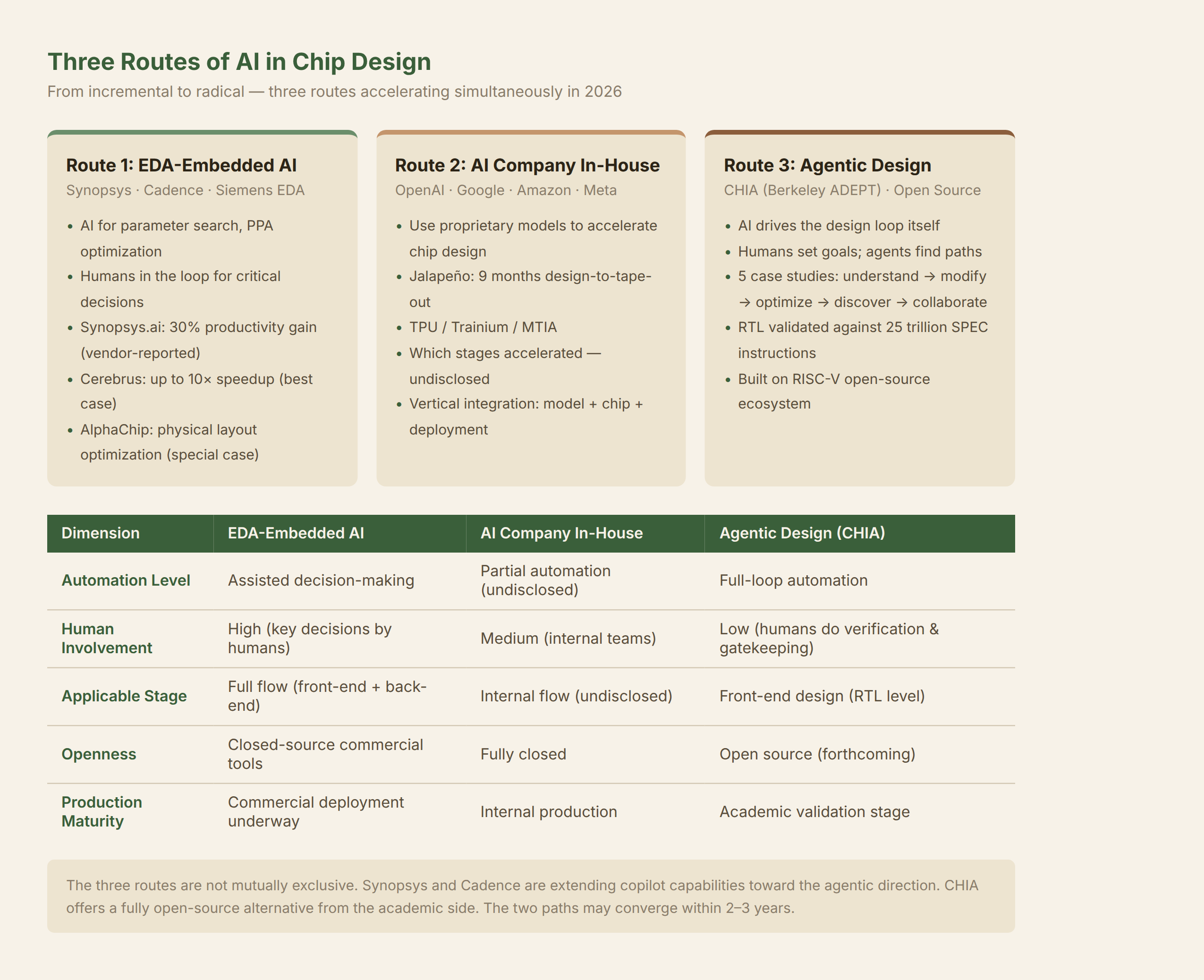
The AI-ification of Chip Design: Three Routes
Before diving into CHIA, you need the full picture of AI in chip design. Three parallel routes are advancing simultaneously:
Route 1: EDA Vendors Embed AI
Synopsys's Synopsys.ai platform claims 30% productivity improvement and 5× development cycle acceleration across the full chip lifecycle (vendor-reported figures). Its core product, DSO.ai, uses AI to search the PPA (power-performance-area) optimization space. Cadence's Cerebrus automatically runs Innovus flows in parallel, using AI to tune parameters for PPA optimization; the company says some customers have achieved up to 10× productivity gains on RTL and verification tasks (vendor-reported best-case figures). At ICCAD 2025 in late 2025, Cadence formally introduced the concept of "agentic AI-driven chip design" and a vision of L5 autonomous IC design.
This is incremental enhancement of an existing workflow. AI helps with parameter search, placement and routing optimization, timing closure, and test-case generation — but humans stay in the loop for critical decisions. The toolchain hasn't changed; the way of working is changing. Google DeepMind's AlphaChip is another example: using AI for floorplanning optimization, compressing weeks of expert physical design work into hours. It's a special case of Route 1 — applying AI at the physical design stage rather than the front-end design stage.
Route 2: AI Companies Design Their Own Chips
OpenAI's Jalapeño (jointly with Broadcom, 9 months design-to-tape-out), Google's TPU, Amazon's Trainium, Meta's MTIA. For these companies, AI capability is itself a chip design tool — OpenAI has stated explicitly that "development was accelerated with assistance from its own models." But which stages were accelerated, and by how much — no public data exists.
Route 3: Agentic Chip Design
This is the direction CHIA represents. Not AI assisting humans in design, but AI driving the design loop itself. The human shifts from "executor" to "quality gatekeeper" and "goal definer."
The three routes are not mutually exclusive. Synopsys and Cadence are extending Route 1's copilot capabilities toward Route 3's agentic direction. CHIA, from the academic side, provides a fully open-source, composable framework that lets any researcher experiment with Route 3.
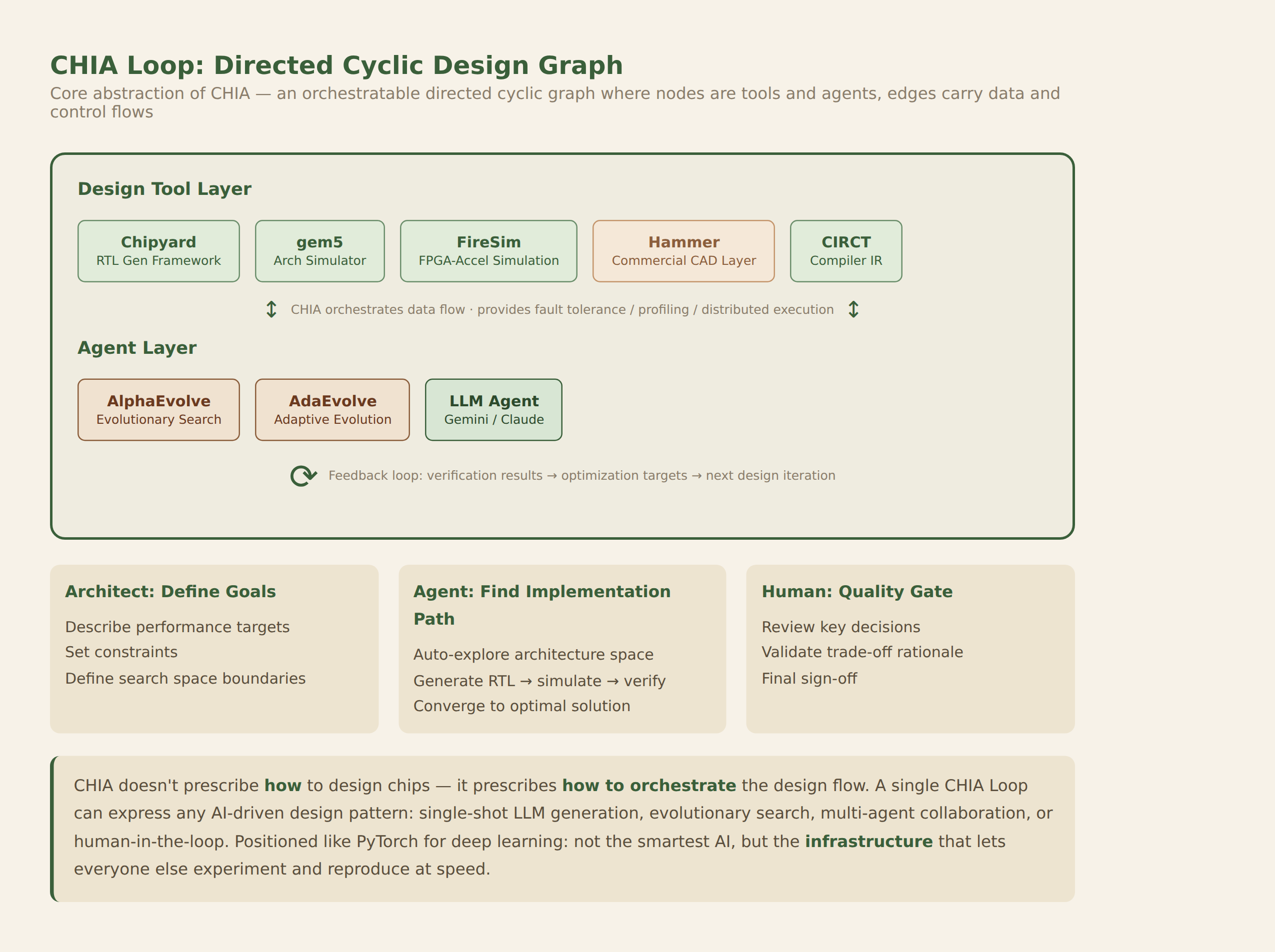
CHIA's Core Abstraction: The Loop as Design Flow
CHIA stands for "Co-designing Hardware/software with Intelligent Agents." The author team consists of core Berkeley ADEPT members: Yakun Sophia Shao, Borivoje Nikolić, Christopher Fletcher, Sagar Karandikar — the same people who built Chipyard, FireSim, and gem5, the infrastructure that much of the RISC-V research community runs on.
CHIA's core abstraction is called the CHIA Loop: a directed cyclic graph whose nodes are chip design tools (Chipyard, gem5, FireSim), commercial CAD abstraction layers (Hammer), evolutionary search agents (AlphaEvolve, AdaEvolve), and LLMs. The framework orchestrates data flow and control flow between these nodes, providing fault tolerance, profiling, and distributed execution.
The elegance of the abstraction lies in this: it doesn't prescribe how you design a chip — it prescribes how you orchestrate a design flow. A single CHIA Loop can express any AI-driven design pattern — single-shot LLM generation, evolutionary search, multi-agent collaboration, human-in-the-loop.
This solves the most frustrating problem in AI chip design research today: every lab writes its own glue scripts to cobble together various tools, producing results that are neither reproducible nor scalable. CHIA's positioning is analogous to PyTorch for deep learning — not the most intelligent AI, but the infrastructure that enables others to rapidly experiment and reproduce results.
Five Case Studies: From Understanding to Creation
The paper uses five case studies to demonstrate that agents within a CHIA Loop can produce production-grade RTL — validated against over 25 trillion SPEC CPU2006 instructions (equivalent to a BOOM processor running the full SPEC CPU2006 benchmark suite over 200 times, an order of magnitude deeper than typical industrial verification coverage), meeting frequency and area constraints on both open-source and commercial process libraries.
The five cases form a progression, each addressing a long-standing pain point in chip design:
- Understanding existing RTL: An agent automatically generates a gem5 simulator model from BOOM processor RTL source code, solving the classic pain point of RTL-simulator desynchronization — a problem that typically costs an engineer two weeks of manual alignment every time the RTL changes.
- Modifying RTL: An agent implements new microarchitectural features in the BOOM out-of-order superscalar RISC-V processor, passing full SPEC CPU2006 validation while improving frequency and area. The difficulty: inserting a new feature into tens of thousands of lines of RTL where one wrong line crashes the entire pipeline, and SPEC must pass or you start over. The agent pulled it off.
- Optimizing performance: An agent analyzes IPC (instructions per cycle) bottlenecks, identifies critical paths, and reasons across microarchitectural levels to generate optimization proposals. This is effectively asking an agent to act as a performance architect — not just finding hotspots in a profile report, but understanding why each hotspot exists and which layers to fix across.
- Discovering new combinations: Based on AlphaEvolve's evolutionary search, the agent parallel-explores the architectural design space within the CHIA framework and reproduces a 2025 state-of-the-art cache replacement policy. A note: "new" here means new combinations within a known design space, not paradigm-level breakthroughs.
- Integrating into collaboration: An agent autonomously handles GitHub issues for the CIRCT compiler project, understands the compiler IR infrastructure, makes correct modifications, and submits them in a way acceptable to maintainers. This step validates not technical capability, but collaborative capability — whether an agent's patches can be accepted by a human community.
The ordering of these five cases is not arbitrary — from understanding to modification, from modification to optimization, from optimization to discovery, from discovery to collaboration. Each step demands a higher degree of autonomy than the last.
How Far Has Commercial AI-EDA Already Gone?
CHIA is an academic framework, but commercial EDA vendors aren't waiting. Synopsys and Cadence have already deployed AI capabilities in their products, and they have customer data.
Synopsys.ai's product portfolio spans digital design (DSO.ai for implementation search optimization), verification (automated test generation, regression analysis, root-cause identification), and test (optimized test pattern generation). In 2026, a strategic partnership with NVIDIA brought GPU acceleration to engineering compute. The vendor's claimed numbers are "30% productivity improvement across the full lifecycle" and "5× development cycle acceleration." These figures come from the vendor and should be read as marketing claims, but the direction is clear: AI is no longer just a copilot for writing Verilog — it's entering the full engineering workflow.
Cadence formally introduced the L5 autonomous IC design concept at ICCAD 2025. Cerebrus handles digital implementation optimization; Verisium handles verification. Cadence's collaboration with NVIDIA has expanded into agentic AI and digital twins. Semiconductor Engineering convened an industry discussion with Cadence, Synopsys, Siemens EDA, Baya Systems, and ChipAgents. The consensus: everyone is talking about an agentic workflow that spans spec → RTL → verification → physical design → sign-off, not single-point copilots.
The key difference between CHIA and commercial tools: Synopsys and Cadence's AI capabilities are embedded within their own closed-source toolchains. Customers can only use them through vendor-provided interfaces. CHIA is fully open-source, based on the RISC-V ecosystem (BOOM + Chipyard + CIRCT). Researchers can freely modify any part of the pipeline. This means CHIA is better suited for frontier exploration — letting an agent freely modify the instruction set to explore trade-offs — while commercial tools are better suited for incremental optimization in production environments.
This dividing line may blur within 2–3 years. If Synopsys and Cadence open more APIs for external agent invocation, or if CHIA's academic results get commercialized, the two routes will converge.
The China Perspective: A Window for Domestic EDA
China's trajectory in AI-driven chip design is out of sync with the global one, but it has its own window.
An Orient Securities research report dated June 29, 2026, notes that domestic EDA has established relatively clear breakthrough paths in mature nodes, analog full-flow, manufacturing-side EDA, device modeling, yield analysis, and digital verification. Advanced-node full-flow tools remain dominated by Synopsys, Cadence, and Siemens EDA, and are unlikely to be fully replaced in the short term.
For China's domestic EDA, AI isn't a shortcut to leapfrogging, but it is a new value layer. Orient Securities' assessment: once AI enters EDA, it won't simply replace traditional tools. Instead, through automated test-case generation, PPA search, fault localization, and multi-round optimization, it drives higher tool invocation frequency and compute consumption, reinforcing platform stickiness. This implies that EDA's business model will migrate from "selling tool licenses" to "selling AI optimization services."
For domestic chip designers like HiSilicon and UNISOC, open-source frameworks like CHIA offer an additional value: against the backdrop of US export controls restricting access to advanced commercial EDA tools, an agentic design framework built on the RISC-V open-source ecosystem provides a technical pathway that does not depend on Synopsys or Cadence. This pathway currently remains at the academic stage, but its strategic reserve value is already apparent.
The Sober Boundaries
CHIA is not magic. Several boundary conditions need to be stated clearly:
Functional verification ≠ physical verification. The RTL produced by agents passed 25 trillion SPEC instruction functional verification, but functional correctness does not equal post-tape-out viability. Power integrity, signal integrity, thermal distribution, manufacturing variation — these physical sign-off stages (final checks confirming that a chip meets foundry acceptance standards across power, timing, manufacturing variation, and other physical dimensions before tape-out) still require traditional EDA tools and human engineering judgment. CHIA currently covers the front end of design (RTL level), not the back end (physical design level).
Evolutionary search ≠ architectural breakthrough. Evolutionary algorithms excel at local optimization along the Pareto frontier of known architectural spaces. But if the next breakthrough requires leaping outside the current search space — say, from traditional cache hierarchies to near-memory computing — agents cannot "invent" new paradigms on their own. They excel at making trade-offs within known frameworks, not at paradigm restructuring. Case Study 4's "new combinations" recombine cache replacement policy parameters within a known design space, not invent a new cache architecture paradigm.
Academic framework ≠ production line. CHIA will soon be open-sourced, but between an academic framework and a TSMC production line lies a vast amount of engineering work: deep integration with commercial PDKs, alignment with foundry process parameters, and the full complexity of physical design. The paper itself acknowledges that the case studies are not exhaustive demonstrations.
Where CHIA Doesn't Reach: AI Is Designing Radio Chips That Humans Couldn't Even Imagine
CHIA's current boundary stops at the RTL level of digital chips. But that doesn't mean the boundary of AI chip design stops there. In a domain CHIA hasn't touched — analog and RF chip design — something even more radical is unfolding.
On June 24, 2026, Princeton University EE associate professor Kaushik Sengupta published a comprehensive retrospective in IEEE Spectrum, "AI Is Designing Radio Chips That Humans Couldn't Even Imagine," summarizing three years of work: AI designing RF integrated circuits (RFICs) from scratch, without any human templates, producing layouts that look like QR codes but outperform state-of-the-art handcrafted designs.
Why RF design is harder to automate than digital RTL. Digital chip design flows are highly standardized — RTL to gate-level netlist to physical layout, each step with mature algorithmic tools. RF design is fundamentally different: it's an engineering contest spanning multiple physical domains. Maxwell's equations govern EM field interactions with active and passive devices across spatial and temporal scales. Thermodynamics dictates heat generation and dissipation. Thermo-mechanical principles determine packaging reliability under temperature swings. Incorporating all physical constraints simultaneously creates a design space that is nearly impossible to manage. Every decision triggers cascading effects — push one corner down, and multiple others pop up.
This is why, for decades, the semiconductor industry has held a consensus: "Digital design is science; RF design is art" — a "dark art" demanding years of experience to master. A veteran RF designer can spend years and tens to hundreds of millions of dollars to complete a single new chip. If any step fails to meet spec — impedance mismatch, thermal density, a passive structure deviating from design — it's back to the beginning.
How AI designs RF chips without templates. Sengupta's team uses a two-phase approach. Phase one: a reinforcement learning framework. The agent explores circuit architecture, topology, device parameters, and even EM interface characteristics from scratch — using zero human-provided circuit templates. Training is analogous to AlphaGo Zero playing against itself rather than learning from human games. Training takes days to a week; once trained, the agent generates a complete new circuit design in minutes. Phase two: a CNN-based AI simulator replaces traditional electromagnetic solvers. Conventional EM simulation software solves Maxwell's equations from scratch — a single iteration can take tens of minutes to hours. The CNN simulator predicts S-parameters directly from structural images, bypassing the underlying physics computation entirely, dropping simulation time from tens of minutes to single-digit milliseconds. The two phases linked together form an end-to-end AI RF chip designer.
How radical are the results. In 2023, the team published a proof-of-concept — a power amplifier for the 30–100 GHz range (covering 5G mmWave and radar bands). The final design achieved the best combination of bandwidth, output power, and efficiency for silicon-based PAs at the time. In 2024, the team demonstrated the method extends to multi-port ICs: traditionally, 16 S-parameters for a 4-port design required days to weeks of simulation; the AI method completes it in minutes. And the most striking finding: there is no evidence that human-designed templates are optimal for modern design goals. AI-generated layouts bear no resemblance to conventional RFIC symmetric geometries — they look more like pixelated QR codes or random patterns — yet the physical prototypes repeatedly outperformed state-of-the-art designs at the time.
What this signal means for chip design. If CHIA proves that digital RTL can shift from manual authoring to agent-driven generation, Princeton's RFIC research proves something else: even the domain considered the least automatable corner of chip design — the "dark art" of analog/RF — has already been breached by AI. And not through incremental optimization, but through generation from scratch.
Taken together, these two events point to a larger assessment: AI chip design isn't penetrating one domain at a time — it's breaking through at both the digital and analog ends simultaneously. This isn't "EDA tools getting smarter." It's "the abstraction level of chip design shifting from RTL/circuit-level to intent-level" — whether CHIA's "human defines goals, agent finds RTL implementation," or Princeton's "human provides S-parameters, AI generates EM structures," the paradigm is the same: the designer moves from executor to goal-definer and verifier.
Of course, Princeton's method has its own boundaries. AI can produce erroneous circuit designs that still require human validation — just as CHIA's "functional verification ≠ physical verification" reminds us, this is not a zero-human system. Sengupta himself notes that data volume remains the bottleneck: without an "ImageNet moment" of large-scale training data, AI RF design's generalization capability remains limited. But this doesn't change the fundamental fact: if even the "dark art" can be automated, there is no corner of chip design AI cannot reach.
The Industrial Implications of Compressed Design Cycles
If agentic chip design becomes practical within 2–3 years, several assessments are worth making early:
The custom chip barrier drops. Broadcom's AI custom chip business generated approximately $20 billion in FY2025 revenue (per Broadcom's financial reports). Its core value proposition is "we customize ASICs for you." If agents automate most of the customization work, the barrier drops from "hire 200 ASIC engineers" to "deploy an agentic design flow + pay the compute bill." Broadcom's client relationships and process expertise won't vanish, but the cost-structure advantage underpinning a $20 billion business will compress — customizing an AI chip no longer requires customizing two hundred people.
A structural tailwind for RISC-V, and the redefinition of the architect's role. These are two related shifts. All five of CHIA's case studies are built on RISC-V — open-source ISA and modular design are a natural fit for agent-driven design exploration; agents can freely modify the instruction set to explore trade-offs, whereas x86 and ARM's closed ISAs constrain the exploration space. Meanwhile, over the past decade, chip design's abstraction level has steadily risen: from transistor to gate-level to RTL to HLS. CHIA lifts abstraction to the "intent level": describe performance goals, and agents find implementation paths. CHIA's paper shows that an agent can complete a full case study end-to-end in hours, while the same work in a traditional design flow typically takes weeks. The most sought-after chip designers of the next decade won't be the best Verilog writers — they'll be the best at using agents to explore architectural space.
From a talent structure perspective, Synopsys's "30% productivity improvement" implies that a 50-person chip design team might shrink to 35 under AI — but the reduction isn't uniform. It cuts 15 junior RTL engineers while adding 1–2 architect-level agent orchestrators. The pyramid base shrinks; the apex becomes taller.
Architects don't write RTL. Architects design loops. When design loops can run in parallel across hundreds of machines, and agents can produce complete RTL validated against 25 trillion instructions in hours — how should the chip architect's skill stack be rewritten?
Synopsys and Cadence are already selling the incremental answer: "30% productivity improvement" — same teams, more output, no fundamental rethinking required. CHIA points to a more radical answer — commercial EDA pursues incremental optimization; open-source academic frameworks pursue radical restructuring. Which one reaches the production line first depends on how far agents can go in physical design and sign-off over the next two years. But whether gradual or radical, the direction is the same: the bottleneck in chip design capability is shifting from "how many people" to "how many good loops you've designed."