
When model weights become part of the silicon, inference no longer requires moving data — computation becomes the wiring itself.
Introduction
On August 4, 2026 (US Eastern Time), AMD announced the acquisition of Taalas, a Toronto-based AI inference chip startup. The deal price was not disclosed. Taalas had raised $219 million in cumulative funding, with a team of 24 people who spent just $30 million to take an 815mm², 53-billion-transistor chip from design through tapeout to a live API.
The deal comes seven months after NVIDIA's ~$20 billion acquisition of Groq's inference assets. Both GPU giants have now placed bets on inference-specialized silicon. The signal is clear: the AI chip competition is shifting from "whose GPU is faster" to "whose inference stack is more efficient."
But Taalas's technical approach differs fundamentally from Groq, Cerebras, and even mainstream GPUs. Understanding this difference is essential to judging what AMD actually bought.
I. Taalas's Approach: Etching Models Into Silicon
1.1 Core Concept: The Hardcore Model
Taalas's design philosophy can be summarized in one line from CEO Ljubisa Bajic:
"The model is The Computer."
Bajic is no stranger to AI chips. He founded Tenstorrent in 2016 (valued at $3.2 billion), pursuing a general-purpose AI chip approach. In 2023, he left to start Taalas, choosing the exact opposite direction — radical specialization. The contrast is itself telling: someone who tried the general-purpose path concluded that specialization is the endgame for inference.
Traditional AI inference works as follows: model weights reside in HBM, and every computation requires shuttling them across a high-speed bus to the compute cores, then back again. This is the classic von Neumann architecture — memory and compute are separated. When model parameter counts reach tens of billions, the data movement itself becomes the bottleneck. In LLM inference workloads, modern GPUs spend a large fraction of their energy and die area moving data rather than computing (estimates vary widely by architecture and workload, generally 60–90%+).
Taalas eliminates this movement entirely. Through a mask ROM process, model weights are etched directly into the chip's metal interconnect layers. Weights are no longer "data being read" — they are the physical structure of the chip.
In implementation, each transistor does not perform arithmetic — it acts as a physical router. The chip pre-computes all possible products for 4-bit quantized values at manufacturing time, physically encoding the results into the silicon interconnect. Transistors simply select the correct pre-computed channel and pass the result to an adder. Bajic's words: "A single transistor can store 4 bits and perform the associated multiply — everything happens in one transistor, and the density is staggering."
The result: storage and computation are physically unified. No HBM, no advanced packaging, no 3D stacking, no liquid cooling, no high-speed I/O.
1.2 Chip Architecture: Dual-Domain Design
The Taalas chip consists of two functional domains:
- Mask ROM domain (immutable): Stores etched model weights. Weights are固化 at tapeout time and cannot be modified at runtime. Changing models requires a new tapeout.
- SRAM domain (mutable): Holds KV cache and LoRA fine-tuning adapters, preserving limited runtime flexibility.
This means the model's "skeleton" (weights) is part of the silicon, while "dynamic state" (context cache, fine-tuning parameters) remains variable. The runtime boundary:
| Dimension | Mutable? | Mechanism |
|---|---|---|
| Base weights | No | Etched in mask ROM |
| Model architecture (layers/heads/dimensions) | No | Hardwired |
| Context window size | Yes | SRAM configuration |
| LoRA adapters | Yes | Loaded in SRAM |
| System prompt | Yes | Passed as input tokens |
| Model version upgrade | No | Requires re-tapeout |
LoRA support is an important flexibility source — customers can apply lightweight behavioral adaptations (tone, domain knowledge, safety policies) on top of a fixed model without re-taping out. But LoRA cannot change the model's base capability ceiling.
1.3 HC1 Specifications and Benchmarks
Taalas released its first test chip, HC1, in February 2026. Official specifications:
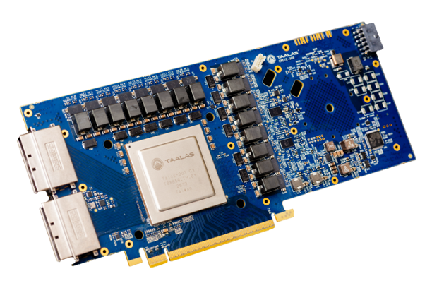
| Parameter | Value |
|---|---|
| Die area | 815 mm² (near reticle limit) |
| Transistor count | 53 billion |
| Process | TSMC 6nm |
| Server power | 2.5 kW/server |
| Model running | Llama 3.1 8B |
| Single-user throughput | 17,000 tokens/sec |
| Quantization | 3-bit + 6-bit mixed |
| Configurable items | Context window size, LoRA fine-tuning |
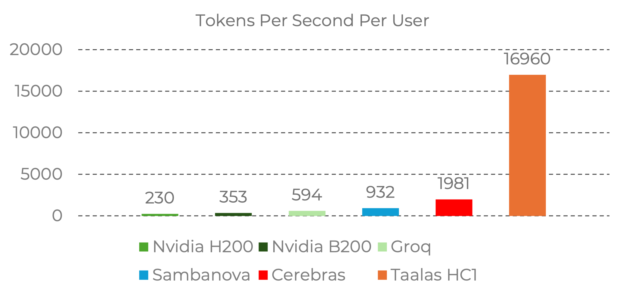
Performance comparison (Llama 3.1 8B, input 1k/1k):
| Platform | tokens/sec/user | Ratio |
|---|---|---|
| Taalas HC1 | ~17,000 | Baseline |
| Cerebras | ~2,000 | HC1 ≈ 8.5× |
| Groq | ~600–800 | HC1 ≈ 20–28× |
| NVIDIA B200 | ~350 | HC1 ≈ 48× |
| NVIDIA H200 | ~200 | HC1 ≈ 85× |
Note: NVIDIA data from official inference guide (H200) and Taalas internal testing (B200); Groq/SambaNova/Cerebras from Artificial Analysis third-party platform; Taalas data from Taalas labs self-testing. Figures reflect the Taalas announcement timeframe; different configurations and software versions may vary significantly. All performance numbers are vendor-reported with no independent third-party verification.
Taalas claims HC1 achieves 20× lower build cost and 10× lower power consumption compared to GPU solutions.
1.4 Cost Structure
Traditional AI inference chip costs stack up from several expensive components: HBM (40–60% of GPU board cost), CoWoS advanced packaging, 3D stacking, liquid cooling infrastructure, and high-speed transceivers. Taalas eliminates all of these, radically simplifying the cost structure.
Bajic claims that etching weights into silicon costs 100× less than training a frontier model. This number needs context: an HC1 chip runs exactly one model (Llama 3.1 8B), while a GPU runs any model. The cost comparison is only fair if you need to run that one specific model for long enough to amortize the tapeout cost.
Taalas states that model updates require "only changing two metal layers." In semiconductor manufacturing, modifying metal layers does not require redoing the front-end transistor process. Mask costs run approximately 10–20% of a full tapeout, with turnaround times of 4–8 weeks. This is much faster than a from-scratch design, but still represents a millions-of-dollars, weeks-long commitment — not something you do casually like a software update.
II. Model Compatibility: What Can Be Etched Into Silicon
This is the critical dimension for evaluating Taalas's feasibility. Taalas claims its Foundry platform can "turn any AI model into custom silicon," but from physical principles and available information, the constraints are clear and multi-dimensional.
2.1 Architecture Constraints
HC1 has validated exactly one architecture: standard Transformer decoder-only. Llama 3.1 8B is the canonical decoder-only Transformer.
If Taalas's Foundry toolchain is truly general-purpose, it could theoretically support other architectures — but each architecture change requires an entirely new chip design:
| Architecture | Feasibility | Notes |
|---|---|---|
| Transformer decoder-only | Validated | HC1 proven |
| Encoder-decoder (T5-type) | Theoretically feasible | More complex compute graph but fixed structure |
| MoE Transformer | Feasible but costly | All experts must physically exist on silicon |
| Mamba / SSM / RWKV | Requires new design | Different computation paradigm |
| Diffusion models | Requires new design | Iterative denoising graph fundamentally different |
The MoE problem is the most critical. Current trillion-parameter MoE models — Kimi K3 (16 activated out of 896 experts), DeepSeek V4 (activated from 384+1 experts) — activate only 3–5% of all experts per inference. On GPUs, inactive experts reside in HBM and are loaded on demand; sparse activation saves computation. But on a Taalas chip, all experts' weights must be physically etched into the silicon — even though only a small fraction is used per inference. MoE's sparse activation advantage is entirely negated by area cost in fixed silicon. A trillion-parameter MoE model would require far more chips than a dense model of equivalent total parameters.
Conversely, dense models are the optimal fit for Taalas — all parameters participate in every inference, so no silicon area is wasted. The Llama family is dense architecture, which is precisely why Taalas chose it for the first product.
2.2 Model Size Limits
Single-chip parameter capacity is bounded by two physical constraints:
- Reticle limit: TSMC's reticle limit is approximately 858mm². HC1 is already 815mm² — nearly at the ceiling. A single chip cannot be made larger.
- Quantization precision: Lower precision means fewer transistors per parameter. HC1 uses 3-bit + 6-bit mixed (averaging ~4 bits/parameter), with 815mm² / 53B transistors hosting 8B parameters. HC2 upgrades to FP4, increasing density with a target of 20B parameters per chip. Precision and density are in direct trade-off: moving to FP8 would roughly double the transistors per parameter, halving the parameter capacity.
The only way to scale model size is pipeline parallelism — distributing different transformer layers across multiple chips. Tokens flow through chip 1's N layers, then to chip 2's M layers, and so on. Fifty HC2 chips (20B each) could theoretically serve a trillion-parameter dense model.
But there is a critical unpublished specification: inter-chip interconnect bandwidth. Pipeline parallelism requires passing KV cache and intermediate activations between chips. If interconnect bandwidth is insufficient, it becomes the throughput bottleneck, wasting the time saved by etching weights. Taalas has never disclosed data here — this is the most significant engineering unknown on the path from concept chip to trillion-parameter deployment.
III. Product Roadmap
Based on Taalas's official information:
| Timeline | Product | Description |
|---|---|---|
| Feb 2026 | HC1 + Llama 3.1 8B | Concept validation; live chatbot (chatjimmy.ai) and inference API |
| Spring 2026 | HC1 + mid-sized reasoning LLM | Second model, still on first-generation silicon |
| Winter 2026 | HC2 + frontier LLM | Second-generation silicon, standard FP4 floating-point, higher density |
Key upgrade: HC1 uses custom 3-bit + 6-bit mixed precision, which Bajic acknowledges introduces "some quality degradation." HC2 adopts standard 4-bit floating-point (FP4), aligning with industry-standard quantization and potentially resolving the precision issue.
HC1's choice of Llama 3.1 8B as the launch model was not because it was the strongest model at the time, but because its small size and open-source availability allowed Taalas to harden it "with minimal logistical effort." This confirms HC1's positioning as a technology demonstration — proving that a model can be etched into silicon and run extremely fast.
Taalas also provides a live demo (chatjimmy.ai) and an inference API service, letting developers experience 17K tokens/sec latency firsthand. This "let developers use it first" strategy suggests Taalas wants to cultivate an application ecosystem before chips reach mass production.
IV. Design Philosophy: Three Principles
Bajic articulated three design principles in his official article:
Principle 1: Total Specialization
"AI inference is the most critical computational workload humanity has ever faced, and the one that stands to gain the most from specialization."
Every model deserves its own optimal silicon. This mirrors the bitcoin mining trajectory: once the algorithm fixed, ASICs entirely displaced GPUs. Taalas bets that AI inference will experience the same "ASIC moment."
Principle 2: Merging Storage and Computation
"By unifying storage and compute on a single chip at DRAM-level density, our architecture far surpasses what was previously possible."
Mask ROM achieves DRAM-level storage density without refresh cycles, without HBM stacking, without high-speed I/O interfaces. Weights do not need to be moved because they are the wiring itself.
Principle 3: Radical Simplification
"The result is a system that does not depend on difficult or exotic technologies: no HBM, no advanced packaging, no 3D stacking, no liquid cooling, no high-speed I/O."
Engineering simplification drives order-of-magnitude reductions in total system cost. Taalas chips can be manufactured on a mature process (6nm) and operate with standard air cooling, entirely avoiding the most congested links in the AI chip supply chain — HBM capacity, CoWoS packaging, liquid cooling infrastructure. This is not only a cost advantage but a supply chain resilience advantage.
V. AMD's Integration Strategy
AMD's official press release rewards close reading:
"Taalas' technology will complement AMD's full-stack AI platform, including AMD Helios rackscale solutions, AMD Instinct GPUs, AMD EPYC CPUs, AMD ROCm software."
The key word is complement, not replace. AMD does not intend to swap out Instinct GPUs for Taalas — it is adding an entirely new accelerator type to the Helios rack.
5.1 PD Disaggregation: Two Horses Already in the Race
Prefill-Decode disaggregation is a major inference optimization trend: the Prefill phase processes the entire input sequence in one parallel pass (compute-bound), while the Decode phase generates tokens one at a time autoregressively (memory-bandwidth-bound). Mainstream frameworks — vLLM, TensorRT-LLM, SGLang — all natively support PD disaggregation.
AMD already has a public partner in this space: on July 22, 2026, at Advancing AI 2026, AMD announced a推理 partnership with Cerebras — Helios racks handle Prefill, Cerebras WSE handles Decode. Cerebras stores weights in on-chip SRAM, offering faster decode than HBM-based solutions while still allowing model switching.
Taalas's role must be understood against this existing Cerebras partnership. The two are not simple substitutes — they target different points on the efficiency-flexibility spectrum:
| Dimension | Cerebras WSE | Taalas MSIC |
|---|---|---|
| Weight storage | On-chip SRAM (reloadable) | Mask ROM (fixed) |
| Model switching | Supported | Not supported |
| Single-model efficiency | High | Extremely high |
| Target use case | Flexible model switching | Ultra-large-scale fixed deployment |
| Supply chain | Wafer-scale chip (hard to manufacture) | Standard process (simple to manufacture) |
Likely positioning: Cerebras for scenarios requiring moderate model-switching frequency (e.g., CSP multi-tenant inference), Taalas for single-model ultra-large-scale deployment (e.g., Meta's Llama inference infrastructure). AMD is hedging across both paths to cover a wider customer spectrum.
5.2 Tick-Tock Deployment Model
Another possible integration pattern: customers first deploy and validate a model on Instinct GPUs, then commit to a Taalas hardened version once confirmed. GPUs handle "flexible validation"; Taalas handles "efficient production."
This model reduces customer fear of model lock-in. You are not betting on whether a chip can run your model — you validate on general-purpose GPUs first, then decide whether to invest in custom silicon. Taalas claims a two-month turnaround from receiving a model to hardware realization, making a tick-tock rhythm commercially viable.
5.3 Rack-Level Differentiation
AMD's acquisition puzzle from 2024 onward is closing:
| Acquisition | Date | Amount | Strategic role |
|---|---|---|---|
| Silo AI | Aug 2024 | $665M | Model development and adaptation |
| ZT Systems | Aug 2024 | $4.9B | Rack-level system integration |
| MK1 | Nov 2025 | Undisclosed | Inference software stack |
| Taalas | Aug 2026 | Undisclosed | Inference-specialized silicon |
Over two years and four acquisitions, AMD has assembled a complete heterogeneous inference stack: from model adaptation to rack integration to inference software to specialized silicon.
NVIDIA's strategy: GPU + NVLink + InfiniBand for full-stack lock-in. AMD's strategy: EPYC CPU + Instinct GPU + Cerebras WSE + Taalas accelerator + ROCm software, delivering heterogeneous inference within the Helios rack.
Lisa Su said at Advancing AI in July 2026: "I firmly believe there is no one-size-fits-all solution in silicon." This is becoming AMD's product philosophy.
VI. Key Risks
6.1 Model Fixation vs. Iteration Speed
Taalas's biggest constraint: model weights are fixed in silicon. Changing models requires re-tapeout. Even modifying metal layers is a weeks-long, millions-of-dollars commitment (see §1.4).
The prerequisite is clear: models must be sufficiently stable. Specifically, Taalas's approach naturally filters its addressable models — large-scale dense Transformers are the best fit. MoE models suffer because all experts must physically exist on silicon, eliminating the area efficiency advantage of sparse activation (see §2.1).
If frontier model architectures undergo fundamental changes every few months — Transformer to Mamba/SSM, dense to MoE — then silicon fixation can never catch up with model evolution.
6.2 The Quantization Ceiling
HC1 uses 3-bit + 6-bit mixed precision, which Bajic acknowledges introduces "quality degradation." HC2's upgrade to standard FP4 will help, but whether 4-bit is sufficient for complex reasoning, long chain-of-thought, and code generation remains an open question.
Google, NVIDIA, and AMD's own GPU inference are all standardizing on FP4, but mainstream production environments still treat FP8/INT8 as the precision floor. If certain workloads genuinely require FP8 or higher, Taalas loses competitiveness there — and increasing precision means more transistors per parameter, reducing the parameter capacity per chip.
6.3 Scaling Engineering Challenges
A 24-person team spending $30 million to produce the HC1 concept chip is a remarkable achievement, but the gap between concept chip and mass-production product is enormous:
- HC1 only runs Llama 3.1 8B (8 billion parameters), while current frontier models are in the hundreds of billions to trillion-parameter range
- Multi-chip pipeline parallelism interconnect is undisclosed — the most critical engineering unknown for trillion-parameter deployment (see §2.2)
- Batch size support is unknown — 17K tokens/sec is a single-user figure; multi-user concurrent throughput is unpublished
- No independent third-party benchmark verification exists
6.4 Customer Profile Constraints
Taalas's approach naturally filters its customer base:
- Suitable: Large model companies' flagship dense model hardened versions, CSP high-frequency standardized API calls, national-scale AI infrastructure
- Unsuitable: Service providers needing frequent model switching, research institutions, multi-tenant model platforms, model services using MoE architectures
The market ceiling depends on "how many customers are willing to pay for single-model extreme inference efficiency."
VII. Competitive Landscape
7.1 The Inference Accelerator Spectrum
Current inference accelerators arrayed on the flexibility-efficiency axis:
| Approach | Flexibility | Efficiency | Weight storage | Example |
|---|---|---|---|---|
| General-purpose GPU | Highest | Lowest | HBM | NVIDIA H100/B200 |
| Dataflow architecture | Medium | Medium-high | SRAM | Groq LPU, Cerebras WSE |
| Programmable ASIC | Low | High | HBM/DRAM | Google TPU |
| Model-fixed ASIC | Lowest | Highest | Mask ROM | Taalas MSIC |
Groq and Cerebras store weights in SRAM — far faster than GPU's HBM, but still requiring on-chip data movement. Taalas physically etches weights into silicon, eliminating movement entirely — higher theoretical efficiency ceiling, but each chip runs exactly one model.
Notably, Groq and Cerebras are now absorbed into NVIDIA and AMD's respective inference product lines. The inference chip competition is shifting from "startups vs. GPU giants" to "NVIDIA ecosystem vs. AMD ecosystem."
7.2 NVIDIA vs. AMD: Diverging Inference Strategies
NVIDIA's acquisition of Groq (~$20 billion, structured as non-exclusive technology licensing + team absorption) added dataflow architecture capability — Groq chips can still run different models by reloading weights. AMD partnered with Cerebras for SRAM-based efficient decode capability, then acquired Taalas for model-fixation capability — each chip runs one model, but an order of magnitude more efficient.
Three paths, three bets:
- NVIDIA bets customers need "flexible enough high-efficiency inference" → Groq path, widest coverage
- AMD-Cerebras bets customers need "switchable high-efficiency decode" → SRAM path, middle ground
- AMD-Taalas bets some customers need "inflexible but extreme-efficiency inference" → fixation path, specialized scenarios
The three are not mutually exclusive. If models converge, Taalas's approach gains unique competitiveness in large-scale fixed deployment. If models keep iterating rapidly, flexible approaches remain safer.
VIII. Assessment
8.1 Short Term (12–18 months)
Taalas technology is unlikely to ship as a standalone product. More probable directions:
- AMD positions Taalas as an optional decode acceleration module within Helios racks, offered alongside the Cerebras solution
- Prioritize ROCm software stack adaptation so Taalas chips can be scheduled by inference frameworks
- HC2 mass production timeline (officially "winter") may shift due to acquisition integration
- First customer engagements likely with existing Helios-deployed Tier-1 customers
8.2 Medium Term (2–3 years)
If HC2 delivers on "FP4 + higher density," AMD can offer a全新的 procurement option: semi-custom inference racks. Customers select a model; AMD + Taalas etch it into chips integrated into Helios racks, delivering inference at far lower TCO than pure-GPU solutions.
This business model resembles Google's TPU — custom chips for specific models — but offered to external customers. The key prerequisite: the target model must be dense architecture and sufficiently stable. If MoE becomes the dominant frontier model architecture (as Kimi K3 and DeepSeek V4 already demonstrate), Taalas's appeal diminishes — unless Taalas finds a way to efficiently support MoE sparse activation on fixed silicon.
8.3 The Deeper Signal
This acquisition reflects a core trend: the AI chip industry is bifurcating into two independent technology stacks — training and inference.
Training market: GPUs remain the only choice because training requires continuously updating weights. NVIDIA's CUDA ecosystem moat is nearly insurmountable on this side.
Inference market: Multiple technology paths are competing in parallel — GPUs (general-purpose), dataflow LPU (semi-specialized), TPUs (programmable ASICs), MSICs (model-fixed). Each finds its position in a different latency-cost-flexibility triangle.
AMD is not buying a chip — it is buying a fundamentally new inference paradigm. Whether this paradigm holds depends on two judgments:
- Will frontier models become stable enough at some point that fixing them in silicon is a reasonable investment?
- Will dense architecture remain the dominant deployment form, or will MoE's sparse activation become the absolute mainstream?
Taalas's team clearly believes the answer is yes. AMD's acquisition is a vote of confidence. NVIDIA's $20 billion Groq deal is a more moderate version of the same bet.
If models are indeed converging — and dense architecture remains important for mainstream inference — then Taalas represents not an edge experiment, but one of the endgame forms of inference infrastructure.
Sources: Taalas official website (taalas.com), AMD Newsroom (newsroom.amd.com), Artificial Analysis platform, The Next Platform. All performance figures are vendor-reported with no independent third-party verification. Not investment advice. Data as of August 7, 2026.