Seoul, June 24, 2026. Corning unveiled a product at the AI Data Center Optical Communication Conference with a gentle-sounding name — GlassBridge. But beneath the name lies a technology that targets the single most stubborn production bottleneck in CPO (Co-Packaged Optics): the mode field mismatch between optical fiber and photonic chips.
CPO has been billed as "coming to production soon" for years but never truly arrived. Not because of electrical design challenges, but because of a few millimeters of glass at the coupling interface. How does Corning solve this with a piece of glass? What is the physics behind it? What does it replace, and what does it leave untouched? And what does it mean for the optical communication supply chain?
This article starts from first principles, working through the complete optical module transceiver path, the physics of the coupling problem, the dead ends of existing solutions, Corning's GlassBridge approach, and finally the supply chain implications and production capacity outlook.
1. The Optical Module's Fundamental Problem: How Electricity Becomes Light and Back
Before GlassBridge, a basic understanding of the optical module's core function — "electrical→optical→electrical" conversion — is essential.
Transmitter Side: Modulating an Optical Carrier with Electrical Signals
The transmitter consists of three components:
The signal flows through four stages: GPU high-speed serial electrical signal → Driver IC (amplifies voltage swing to modulator's required level) → CW Laser (emits continuous-wave light as optical carrier) → Modulator (uses electrical signals to control the carrier's on/off or phase/amplitude) → modulated optical signal enters fiber.
The core modulator device is a Mach-Zehnder interferometer (MZI). The CW laser's continuous light is split into two equal paths. An electrical signal applied to one arm changes that arm's refractive index through the Pockels effect, creating a phase difference between the two paths. When the two beams recombine at the output:
- Phase difference 0° → constructive interference → light output = 1
- Phase difference 180° → destructive interference → light output = 0
The essence: electrical signals controlling light's "on/off" — billions of times per second.
Receiver Side: Converting Light Back to Electricity
The receiver is the reverse process:
The receiver reverses the process through four stages: modulated optical signal from fiber → Photodetector (PD/APD, photons hit the semiconductor PN junction and excite electron-hole pairs; E = hf, photon energy exceeding the bandgap triggers the photoelectric effect) → TIA transimpedance amplifier (amplifies μA-level photocurrent into processable voltage) → DSP (equalization, clock recovery, FEC decoding) → electrical output to GPU.
The PD's physics is the photoelectric effect: each photon excites one electron-hole pair. Light intensity variation converts directly into current pulses; the "1/0" sequence of current pulses is the raw data.
The DSP's Role
The DSP does not handle optical conversion — it is an electrical-domain signal preprocessor. On the transmitter side, it applies pre-emphasis (compensating for fiber dispersion-induced waveform distortion) and FEC encoding (adding redundant error-correction codes). On the receiver side, it performs channel equalization (compensating for bandwidth-limited inter-symbol interference), clock recovery, and FEC decoding.
The complete optical module signal path can be summarized as:
The complete chain in one sentence: GPU electrical → DSP preconditioning → Driver + Modulator + CW Laser (E-to-O conversion) → fiber transmission → PD + TIA (O-to-E conversion) → DSP postprocessing → GPU electrical. Every function in an optical module serves this chain.
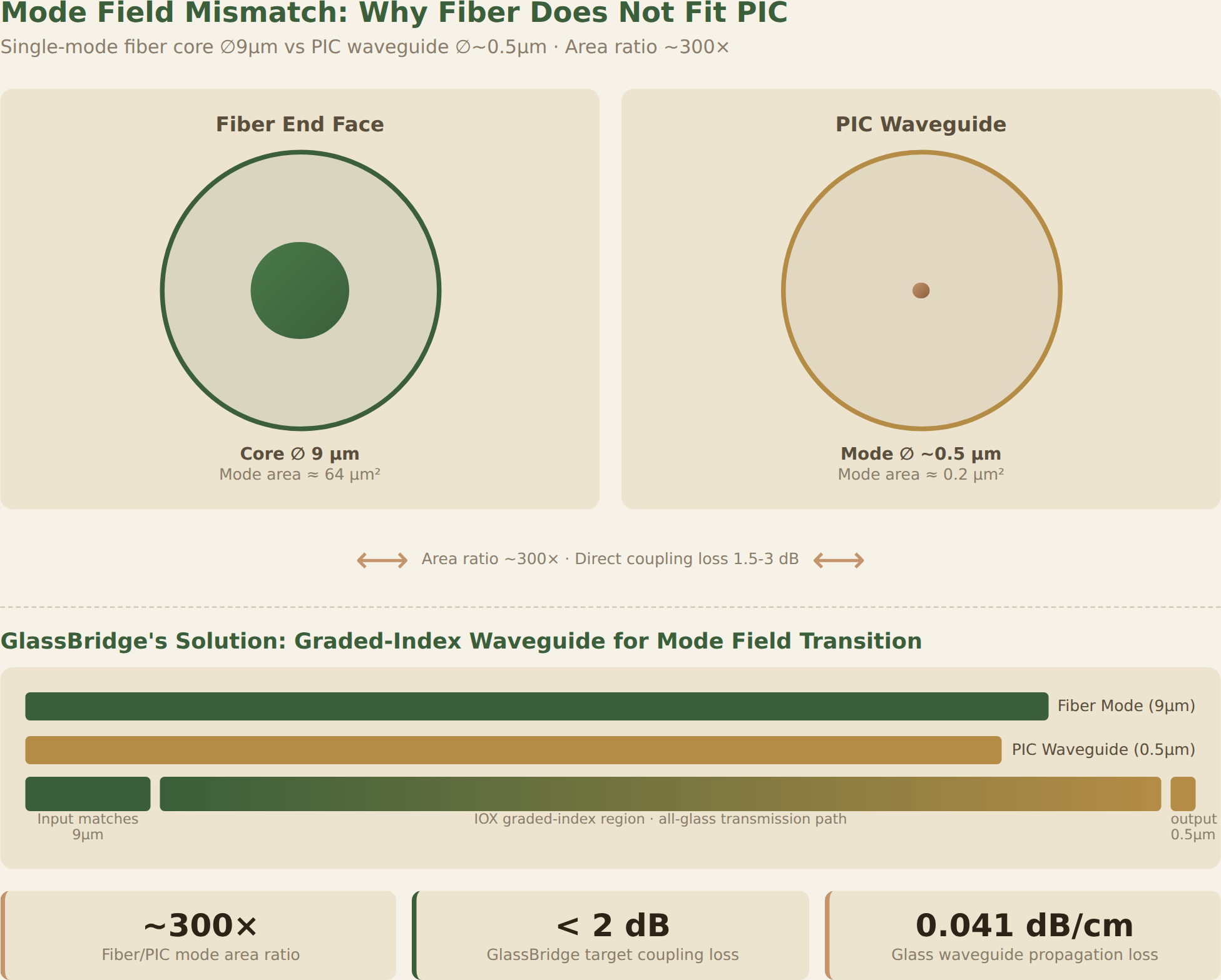
2. The Physics of the Coupling Problem: 9 Micrometers vs 0.5 Micrometers
The optical module's transmission path contains many loss points. Fiber itself is extremely low-loss (0.2 dB/km), but the coupling stage between fiber and chip is where the heaviest losses concentrate.
Mode Field: Light's Effective Cross-Section in a Waveguide
When light propagates in a waveguide, energy is not concentrated on a geometric line but distributed across a cross-section — the "mode field."
| Transmission Medium | Mode Field Diameter | Relative Scale |
|---|---|---|
| Standard single-mode fiber core | 9 μm | 1 |
| Silicon photonic (PIC) on-chip waveguide | ~0.5 μm | 1/18 |
| Mode area ratio | — | 1:324 |
Directly butting the 9μm fiber end face against the 0.5μm chip waveguide end face causes most of the light energy to spill outside the waveguide — the same physics as attaching a fire hose to a drinking straw.
The Cost of Coupling Loss
Coupling loss is measured in dB. 3 dB = 50% of light energy lost. Traditional edge coupling typically suffers 1.5-3 dB loss, meaning 29% to 50% of the optical energy is lost the instant it transitions from fiber to chip.
The direct consequence: to ensure the receiver can still discern the signal, the transmitter must boost laser power. CW lasers have only 10-20% electrical-to-optical conversion efficiency. Each 1.5 dB of coupling loss (about 29% optical power loss) requires the laser to output 41% more optical power, correspondingly increasing electrical power by about 41%. Going from 1.5 dB to 3 dB means electrical power doubles. CPO's entire value proposition is power savings — if coupling loss consumes the power saved by co-packaging, the architecture's fundamental justification erodes.
Why Not Just Use a Wider Waveguide?
Technically, a wider on-chip waveguide could be designed to match fiber, but this sacrifices another critical parameter — integration density. Wider waveguides occupy more chip area, reducing the number of channels that can be integrated and the density of MOE devices (modulators, detectors, etc.).
The only answer: perform mode field conversion between fiber and chip — smoothly transitioning the 9μm mode down to 0.5μm.
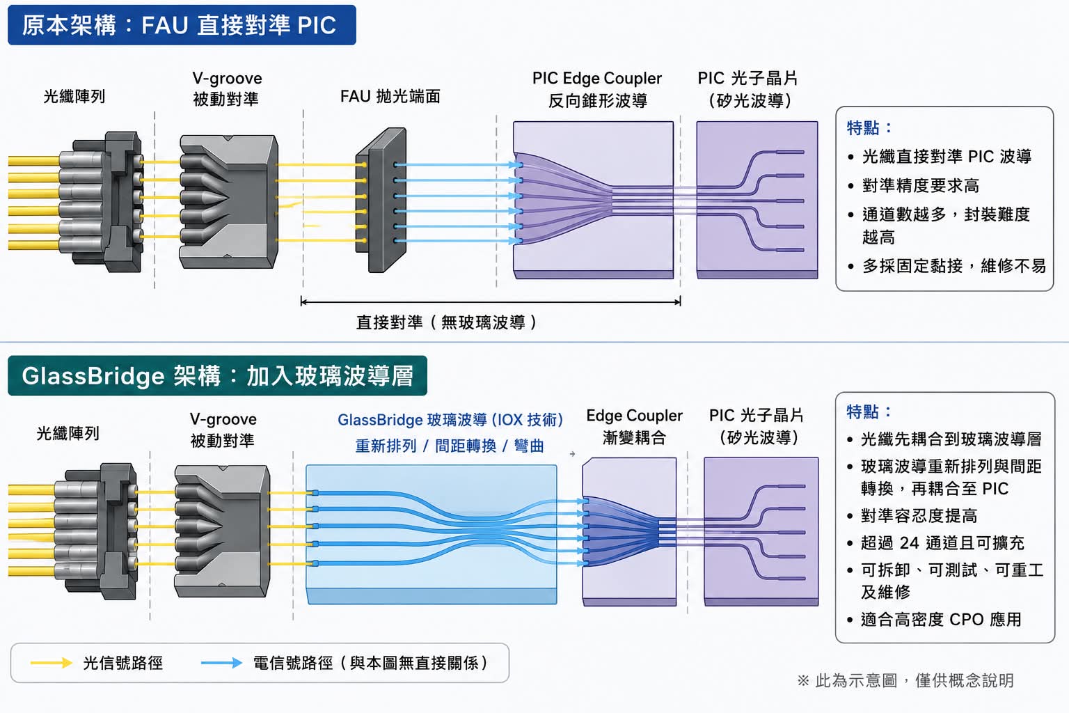
3. The Traditional Solution: FAU's Process Difficulties
What Is FAU?
FAU (Fiber Array Unit) is the standard component for performing mode conversion and fiber alignment. It mounts N fibers precisely in a V-groove substrate, bonding their end faces to the PIC's N waveguide ports.
FAU manufacturing steps:
- V-groove fabrication: Anisotropic wet etching on silicon creates V-groove arrays with <1μm pitch accuracy
- Fiber installation: Bare fibers placed into V-grooves one at a time, each channel independently aligned
- End face polishing: Entire end face ground and polished to nanometer flatness
- Lens shaping: Some designs polish fiber ends into wedges or integrate lenses for initial mode conversion
- Active alignment: FAU and PIC placed on six-axis precision stages; live optical power feedback finds optimal position, then UV-cured
Active Alignment Precision Requirements
FAU-to-PIC alignment requires: position error <0.1μm, polarization axis error <0.5°. This demands sub-micron precision stages, laser interferometer feedback, and high-magnification microscopy closed-loop control — each alignment tool costs millions of RMB and processes a limited number of modules per hour.
Three Structural Deficiencies
Deficiency 1: Non-repairable. FAU and PIC are permanently bonded. In CPO, the optical engine and switch chip are co-packaged on one substrate, with FAU bonded permanently to the PIC front end. If any of 64 channels fails (broken fiber, dead PD), the entire substrate must be scrapped. No cable-replacement possible.
Deficiency 2: Yield cliff. Assuming 98% per-channel alignment success, 24-channel simultaneous success = 0.98²⁴ ≈ 61.6%. Adding thermal stress from UV cure shrinkage and transport vibration, HVM yield at high channel counts can fall below 50%.
Deficiency 3: Density ceiling. FAU channel pitch is constrained by fiber cladding diameter (125μm), with V-groove pitch physically limited to ~127μm. Next-generation CPO requiring 64+ channels at higher density cannot physically fit into 127μm spacing.
Source: Corning ECTC 2026 technical paper / GlassBridge product launch materials
4. GlassBridge: Moving Alignment Inside the Glass
Core Concept Shift
FAU's approach: align mechanically outside the glass — precision depends on equipment and process, fibers aligned one at a time, non-repairable.
GlassBridge's approach: pre-bury the optical path inside the glass — mode conversion between fiber terminal and PIC waveguide is automatically completed by the graded refractive index waveguide inside the glass. Precision is guaranteed by wafer-level lithography, performing all channel alignment simultaneously.
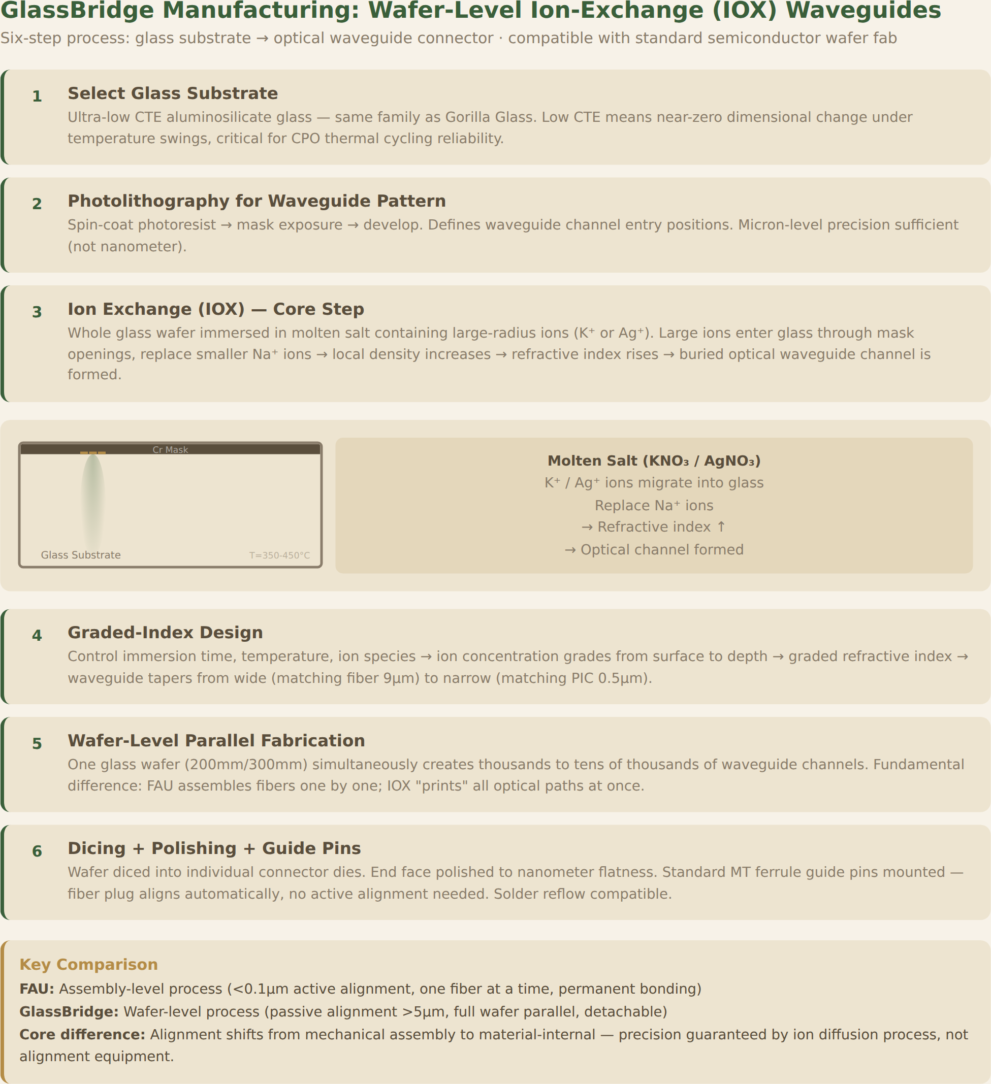
Ion-Exchange (IOX) Waveguide Process
The process has six steps:
Step 1: Glass substrate selection. Ultra-low CTE aluminosilicate glass — same Gorilla Glass family. Low CTE means near-zero dimensional change under temperature swings, critical for CPO thermal cycling reliability.
Step 2: Photolithography for waveguide patterns. Spin-coat photoresist → mask exposure → develop. Same principle as semiconductor photolithography, but micron-level precision suffices (not nanometer), since optical waveguides do not require transistor linewidths.
Step 3: Ion exchange (IOX). The entire glass wafer is immersed in molten salt. Large-radius ions from the molten salt (K⁺ or Ag⁺) enter the glass through mask openings, replacing the glass's original smaller Na⁺ ions:
Large-radius ions (K⁺ or Ag⁺) from the molten salt enter the glass through mask openings, replacing the glass's original smaller Na⁺ ions. The replacement increases local glass density and refractive index, forming a buried optical channel inside the glass. Light in a medium always follows the highest refractive index path (Fermat's principle) — a channel with refractive index higher than its surroundings constrains light to propagate within it, identical to how fiber guides light (core index > cladding → total internal reflection confines light to the core).
Step 4: Graded-index design. By controlling immersion time, temperature, and ion species, ions diffuse from the surface inward with concentration decaying with depth → refractive index grades from surface to depth, creating a waveguide that tapers from wide to narrow:
By controlling immersion time, temperature, and ion species, ions diffuse from the surface inward with concentration decaying with depth. The refractive index grades correspondingly, creating a waveguide that tapers from wide to narrow: the input end matches the fiber's 9μm mode field, the output end converges to the PIC's 0.5μm mode field, with a smooth graded-index transition in between — no abrupt interface, no reflection loss.
Step 5: Wafer-level parallel fabrication. One glass wafer (200mm/300mm) simultaneously creates thousands to tens of thousands of waveguide channels. FAU assembles fibers one by one; IOX "prints" all optical paths at once — a fundamental efficiency difference.
Step 6: Dicing, polishing, guide pins. The wafer is diced into individual GlassBridge connector dies. End faces polished to nanometer flatness. Standard MT (Mechanical Transfer) ferrule guide pins mounted — when the fiber plug is inserted, the guide pins self-align, no active alignment needed.
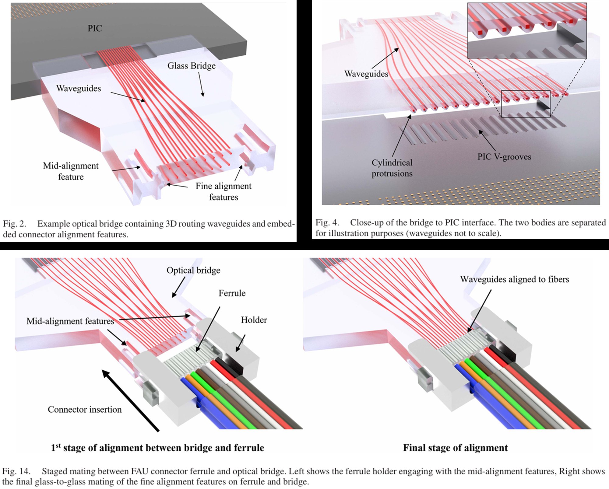
Source: Corning ECTC 2026 technical paper. Fig.2: optical bridge with 3D routing waveguides (left); Fig.4: bridge-to-PIC interface close-up showing cylindrical alignment features and PIC V-grooves (top-right); Fig.14: staged mating between FAU connector ferrule and optical bridge — coarse alignment triggers fine alignment (bottom)
Why Passive Alignment Is Sufficient
GlassBridge's alignment tolerance comes from the design of its two interfaces:
Fiber→GlassBridge: The input waveguide entry is made slightly wider than the fiber core (IOX diffusion width can be controlled), so the 9μm fiber mode can shift ±5μm and still fully enter the waveguide. Standard MT ferrule guide pin positioning precision is about ±5μm — just sufficient.
GlassBridge→PIC: This interface is glass waveguide end face directly contacting the PIC waveguide end face. Both are planar surfaces (not a fiber arc against a chip plane), providing larger contact area. The GlassBridge and PIC are passively aligned once during pick-and-place (positioning accuracy ~10μm sufficient, no six-axis active alignment needed). After that, the guide pin structure handles fiber insertion without moving the PIC interface.
How Detachability Works
The GlassBridge's MT interface is physically pluggable — the fiber terminal (using standard MT ferrule) can be removed and replaced. This directly solves FAU's non-repairable pain point. The CPO module's maintenance model shifts from "any channel fails → full module scrap" to "fiber fails → replace cable."
GlassBridge's Limitations
Corning's official clarification has three points:
- GlassBridge covers only the centimeter-scale fiber-to-PIC coupling. It does not replace external transmission fiber. Fiber demand continues growing, independent of GlassBridge.
- 2026-2027 is sample validation only — hyperscaler validation cycles take at least 12-18 months. 2028 is the true volume production inflection point.
- Corning continues to expand its FAU product line. If FAU were obsolete, Corning would not invest in expanding FAU capacity.
5. Key Performance Metrics
Data from Corning's ECTC 2026 paper and the June 24 launch:
| Metric | GlassBridge | Traditional FAU Edge Coupling | Significance |
|---|---|---|---|
| Waveguide propagation loss | 0.041 dB/cm | — | Intrinsic substrate loss extremely low |
| Bending loss | ~0.01 dB/cm | — | High routing flexibility |
| Single fiber↔PIC loss (TE mode) | 1.44-1.75 dB | 1.5-3 dB | Low end comparable, high end significantly improved |
| Full path loss (both coupling faces + glass WG) | <2 dB | >3 dB common | Can reduce ELS power ~2× |
| Channel pitch | 30μm (scalable) | 127μm (FAU limit) | 4×+ density improvement |
| Channels per component | 24+ | 12-24 (yield drops sharply) | Enables next-gen high-density CPO |
| Alignment method | Passive (guide pins) | Active (six-axis) | Equipment cost dramatically reduced |
| Assembly yield | >90% | <50% at high density | Directly impacts CPO production economics |
| Repairability | Detachable | Permanent bond | Huge maintenance cost difference |
| Solder reflow compatible | Yes | No | Compatible with standard SMT (Surface Mount Technology) process |
Note: "Single fiber↔PIC loss" refers to optical signal traveling from one fiber through GlassBridge into a single PIC waveguide path. "Full path loss" refers to the complete fiber array → GlassBridge mode conversion → PIC coupling path. These two metrics measure different scopes, drawn from component-level and module-level data respectively in the ECTC 2026 paper.
Table interpretation: GlassBridge's core advantage is not overwhelming superiority in any single metric — propagation loss and coupling loss are incremental improvements. The real differentiators are manufacturability dimensions: passive alignment + detachability + high yield. What CPO needs to go from lab to fab is not "lower loss" but "acceptable cost at production volume."
6. GlassBridge's Exact Position in the CPO Optical Path
The complete CPO optical path, from GPU electrical to far-end fiber:
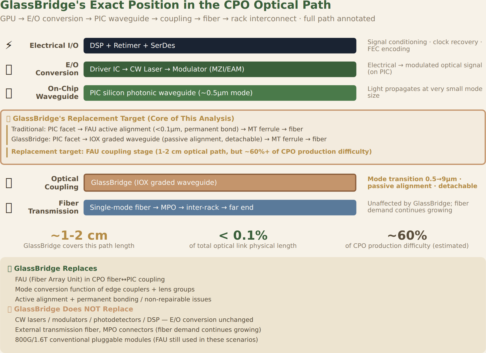
GlassBridge replaces the FAU-to-PIC facet interface — an optical path of about 1-2 centimeters. This is less than 0.1% of the total optical link's physical length, but it is the most difficult, most expensive, and most fragile stage in CPO production.
It does NOT replace:
- Lasers, modulators, photodetectors, DSP — E/O conversion function unaffected
- Fiber jumpers and MPO (Multi-fiber Push-On) connectors — external transmission unchanged
- 800G/1.6T conventional pluggable modules — FAU still used in these scenarios, GlassBridge targets only CPO high-density needs
7. Supply Chain Impact by Tier
Definite Beneficiaries
| Segment | Representative Companies | Logic |
|---|---|---|
| CW light sources | Yuanjie, Lumentum, Coherent | GlassBridge reduces coupling loss → same power supports more channels / lower ELS (External Light Source) power for same channels → light source demand grows |
| TFLN (Thin-Film Lithium Niobate) modulators | Guangku Technology (one of three global suppliers) | CPO density increases → modulator integration density grows |
| High-speed EMLs (Electro-absorption Modulated Lasers) | Changguang Huaxin | Core laser device for CPO and 1.6T+ modules |
| High-precision alignment inspection equipment | RoboTechnik (ficonTEC, key global supplier) | GlassBridge still needs inspection equipment for final alignment verification |
Core Position
| Company | Position Logic |
|---|---|
| Huagong Technology | 3.2T CPO architecture + TGV glass substrate manufacturing equipment |
| Hengtong Optoelectronics | Full silicon photonics stack + polarization-maintaining fiber |
| Zhongji InnoLight | CPO volume leader |
| Taisun | MPO connector deep partnership with Corning (18 years) |
| Changxin Bochuang | MPO connector + Google core supplier |
Dual-Pressure Tier
| Company | Pressure Source | Buffer Direction |
|---|---|---|
| Tianfu Communication | FAU business in CPO scenario being replaced | Migration to optical engine |
| Shijia Photonics | FAU under pressure | AWG demand growth hedge |
| Tengjing Technology | FAU + OCS dual track | 3-5 year transition window |
The Structural Shift
GlassBridge accelerates standardization of the coupling stage in CPO. Its supply chain impact has a deeper dimension: the manufacturing process for optical path alignment moves from "precision mechanical assembly" (optical module assembly) to "wafer-level semiconductor process."
The people who finish FAU are precision assembly engineers. The last process step for GlassBridge is a wafer dicing saw.
In the CPO era, value in the coupling stage migrates from the assembly side upstream to glass and wafer manufacturing. Traditional optical module companies' moat has been precision optical assembly and test capability. If that capability is replaced by wafer-level IOX processing, the remaining value is only "optoelectronic function chip integration" — requiring a transition to optical engine design, which not all traditional module makers can achieve.
However, a counterpoint is necessary: IOX wafer-level yield ramps and initial cost structure should not be underestimated. Mature FAU assembly lines remain cost-effective in low-channel-count, non-CPO scenarios (800G pluggable modules). GlassBridge's full replacement requires CPO to reach meaningful volume — a transition window that gives traditional module makers at least 3-5 years to reposition.
8. Production Capacity and Timeline
Corning's Capacity Plan
In May 2026, NVIDIA and Corning announced a multi-year partnership. Corning will build three new advanced manufacturing facilities in the US:
- North Carolina: 2 facilities
- Texas: 1 facility
- All dedicated to producing optical connection solutions for NVIDIA
NVIDIA has committed $500 million for immediately exercisable Corning warrants. This is part of NVIDIA's 2026 series of optical interconnect investments (previously $6 billion in Lumentum, Coherent, and Marvell over 30 days).
Production Timeline
| Phase | Time | Key Conditions |
|---|---|---|
| Samples + EVT/DVT | 2026 | Joint validation with hyperscalers (NVIDIA/Meta/Amazon) |
| Small-volume production | 2027 | 1.6T CPO industrial deployment begins |
| Volume production | 2028 | 3.2T CPO industrialization + glass substrate packaging commercial |
| Peak penetration | 2028-2030 | LightCounting projects CPO cumulative market ~$100B total (2028-2030 aggregate, not annual) |
Capacity Constraints
-
IOX yield ramp: Corning is a glass manufacturing giant (Gorilla Glass annual production in hundreds of millions of square feet), but optical-waveguide-grade IOX requires new deposition/diffusion equipment configurations. Yield ramp takes at least 1-2 years.
-
Downstream validation: CPO packaging requires multi-physics (optical/electrical/thermal) joint validation. Hyperscaler selection and validation cycles determine GlassBridge order volume ramp speed.
-
Inspection equipment: RoboTechnik (ficonTEC) high-precision inspection equipment capacity is a potential bottleneck — Corning makes the glass, but downstream alignment and final inspection require specialized equipment.
-
Material supply: The specialty ultra-low CTE aluminosilicate glass formulation depends on Corning's proprietary formulation system. Raw material supply chain readiness for mass production has not been publicly disclosed.
9. Summary
GlassBridge's physics is elegant: the most difficult alignment problem is moved from precision mechanical assembly into a wafer-level material process. A single graded-index waveguide simultaneously performs mode conversion and alignment.
But it is not an "optical module killer" — it is one piece of the puzzle on CPO's path to volume production. Across the five dimensions analyzed in this article, it provides incremental improvements in loss and density, and breakthrough improvements in yield, repairability, and process scalability.
But volume production is still at least two years away. 2026's sample validation, 2027's small-batch ramp, and 2028's volume inflection each depend on actual downstream order decisions from cloud customers. Corning has capacity, has NVIDIA's capital backing, and has basic process validation data. But the ultimate variable determining GlassBridge's penetration is: when will CPO itself truly take off?
Disclaimer: This article is based on Corning's June 24, 2026 Seoul AI Data Center Optical Communication Conference release, ECTC 2026 published paper data, and cross-validated against multiple sources including Orient Securities, Aijian Securities, and Xueqiu. Industry views and supply chain impact judgments incorporate public commentary from multiple industry analysts and the author's own understanding. Market projections reference LightCounting public data. This does not constitute investment advice. Data is current as of June 30, 2026.