I. Opening: The Death of CPX and the Birth of LPU
A Quiet Funeral
March 17, 2026, San Jose, GTC 2026 main stage. Jensen Huang, in his trademark leather jacket, walked onto the stage before twelve thousand developers and analysts, and began his two-hour keynote. He talked about Vera Rubin NVL72, about DGX Cloud, about the future vision of agentic AI. But there was one name — a name that, just six months earlier, NVIDIA had positioned as the strategic core of its "inference-optimized GPU" initiative — Rubin CPX — that was not mentioned once during the entire presentation.
In the post-event slides, Rubin CPX had disappeared from the product roadmap. In its place was an entirely new chip: Groq 3 LPU.
This was not a simple product delay or iterative upgrade. This was a three-trillion-dollar company that, in less than six months, killed its own inference GPU design and replaced it with an architecture built from scratch — on-chip SRAM, no HBM, deterministic dataflow execution. And to do so, NVIDIA paid $200 billion in a licensing-and-acquihire deal.
Timeline: From Launch to Disappearance
- September 2025: NVIDIA unveiled Rubin CPX at the AI Infra Summit — a single-die inference GPU based on the Rubin architecture, equipped with 128 GB of GDDR7 memory, 30 PFLOPS of NVFP4 compute, positioned as a dedicated chip for million-token long-context inference.
- October 2025: At GTC DC (GTC Fall), Rubin CPX appeared in the Vera Rubin platform roadmap. NVIDIA painted a disaggregated serving vision: Rubin GPU handling training and prefill, CPX handling pure decode.
- December 24, 2025: NVIDIA announced the acquisition of Groq's core assets for approximately $200 billion (structured as a licensing + acquihire rather than a legal entity acquisition). Groq CEO Jonathan Ross and the core team joined NVIDIA. This was NVIDIA's largest acquisition to date, a 2.9× premium over Groq's $6.9 billion valuation from September 2025.
- March 2026: At GTC 2026, Rubin CPX vanished from the roadmap. Groq 3 LPU and the LPX Rack replaced CPX as the inference acceleration solution for the Vera Rubin platform.
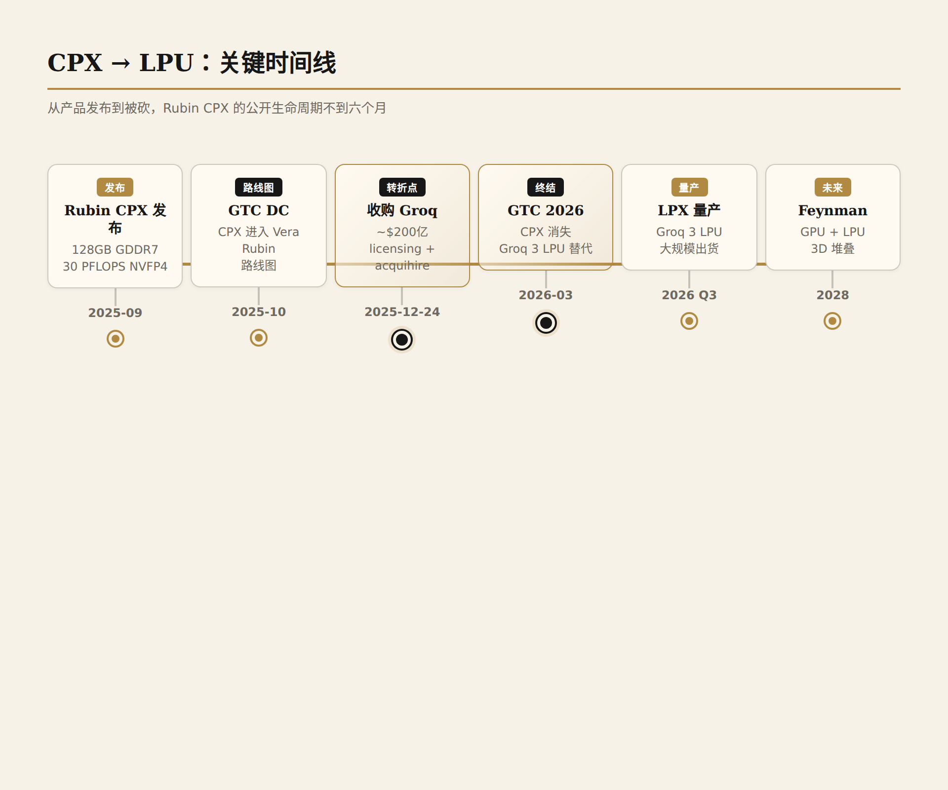
From product launch to cancellation, CPX's public lifespan was less than six months. What happened during those six months is worth examining in depth.
Four Core Questions
This report attempts to answer four questions:
- Why are GPUs inefficient at inference? Is the era of shared hardware for training and inference coming to an end?
- What was CPX's design philosophy, and where did it fall short? Why was NVIDIA's in-house inference GPU solution not good enough?
- What is the architectural essence of the LPU? Why can on-chip SRAM + deterministic execution crush GPUs at inference?
- What does this mean for AI infrastructure? From data center design to the economics of compute, how large is the practical impact of this inference architecture paradigm shift?
This is not just a strategic choice by one company. This is the hardware reflection of the entire AI industry's shift from "training is king" to "inference is king."
II. The Nature of the Inference Bottleneck: Why GPUs Fall Short
Training vs. Inference: Where 90% of the Money Goes
A frequently cited yet still underestimated fact: over the lifecycle of a large language model, 80-90% of compute costs occur during inference, not training.
Consider a GPT-4-class model: training once may cost tens of millions to hundreds of millions of dollars in compute. But once deployed, the model faces hundreds of millions of requests and trillions of tokens generated daily. The cumulative cost of inference quickly surpasses training. The AI inference market is estimated to grow from approximately $106 billion in 2025 to $255 billion by 2030.
Yet until 2025, the AI hardware arms race was almost entirely centered on training. H100, B200, Rubin R100 — every generation of flagship GPU was benchmarked primarily on training performance: higher FP8/FP4 FLOPS, larger HBM capacity, faster NVLink interconnect. Inference was merely an "incidental task" for training hardware.
This became a problem because training and inference have fundamentally different compute patterns:
| Dimension | Training | Inference (Decode Phase) |
|---|---|---|
| Compute pattern | Large-batch matrix multiplication, dense parallelism | Sequential autoregressive generation, serial dependency |
| Bottleneck | Compute (FLOPS) | Memory bandwidth (bytes/s) |
| Batching | Can be very large (thousands of samples processed simultaneously) | Constrained by latency; batch sizes typically small |
| KV Cache | Not needed (all tokens known during training) | Must be maintained; grows linearly with context length |
| Hardware utilization | Compute utilization can reach 60-80% | Bandwidth utilization low; compute utilization often under 10% |
The core contradiction: training is compute-bound; inference (decode) is memory-bandwidth-bound. During training, you can crank up the batch size and keep every CUDA core at full tilt doing matrix operations. During inference, every generated token requires reading the entire model weights and full KV Cache from memory — and each card's bandwidth is fixed.
The Curse of Autoregression
LLM inference (decode phase) has an inherently non-parallelizable characteristic: autoregressive generation.
For every token generated, the model must:
- Use the previous step's output as the new input
- Use the attention mechanism to look up all previous tokens (KV Cache)
- Run a complete forward pass to compute the probability distribution
- Sample to obtain the next token
This process is strictly serial — you cannot begin computing token N+1 before knowing token N.
This means that regardless of how many TFLOPS your chip has, the decode speed ceiling is determined by two things:
- Memory bandwidth: how many bytes per second you can move from storage to compute units
- KV Cache access time: as context grows longer, the data volume to read grows linearly
HBM Bandwidth Bottleneck: A Quantitative Analysis
Let's quantify this problem with real numbers.
Scenario: A 70B parameter model, FP8 precision, inference serving.
- Model weights: approximately 70 GB (FP8)
- KV Cache: depends on context length. For 128K-token context at FP8, approximately 20 GB
- Data to read per decode step: approximately 90 GB (weights + KV Cache)
Decode time estimates on mainstream GPUs (memory read time only):
| GPU | HBM Bandwidth | Time to Read 90 GB | Theoretical Max tokens/s |
|---|---|---|---|
| H100 SXM | 3.35 TB/s | ~27 ms | ~37 |
| B200 SXM | 8 TB/s | ~11 ms | ~90 |
| Rubin R100 (288GB HBM4) | 22 TB/s | ~4 ms | ~250 |
| Groq 3 LPU (SRAM) | 150 TB/s | ~0.6 ms | ~1,600+ |
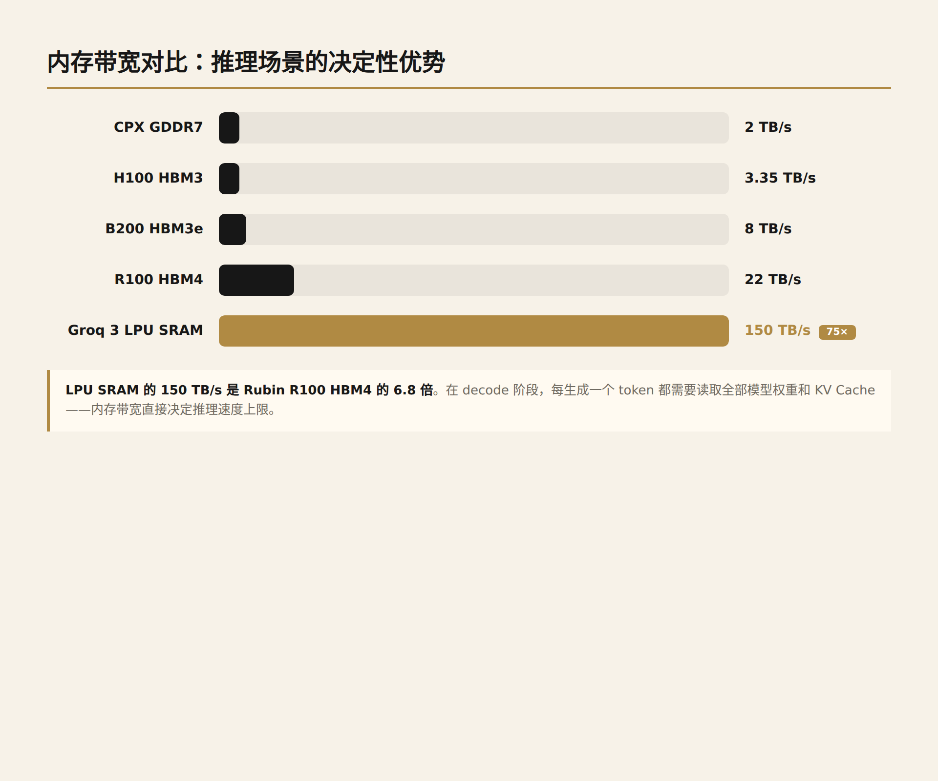
Note that these numbers represent ideal scenarios — actual inference also involves attention computation overhead, software stack scheduling latency, batch management, and so on. But the core conclusion is already clear: at 150 TB/s SRAM bandwidth, even Rubin R100's 22 TB/s HBM4 is nearly 7× slower.
And this is only at 128K context. When context extends to 1M tokens, KV Cache grows to approximately 160 GB at FP8. This means:
- H100: reading 230 GB (weights + KV) takes ~69 ms → theoretical ~14 tokens/s
- B200: reading 230 GB takes ~29 ms → theoretical ~35 tokens/s
- Rubin R100: reading 230 GB takes ~10.5 ms → theoretical ~95 tokens/s
- Groq 3 LPU: reading 230 GB takes ~1.5 ms → theoretical ~650+ tokens/s
The longer the context, the worse the bandwidth bottleneck, and the more pronounced SRAM's advantage.
KV Cache: Exponential Pressure
KV Cache is a memory pressure source unique to inference, and also the most easily underestimated cost factor.
For each token in context, the attention mechanism must store key and value tensors for every layer and every KV head. For a Llama 3 70B-class model (80 layers, 8 KV heads, 128 head dim), the KV Cache size per token is:
2 × 80 layers × 8 heads × 128 dim × 2 bytes (BF16) ≈ 320 KB/token
This means:
| Context Length | BF16 KV Cache | FP8 KV Cache | FP4 KV Cache |
|---|---|---|---|
| 32K tokens | ~10 GB | ~5 GB | ~2.5 GB |
| 128K tokens | ~41 GB | ~20 GB | ~10 GB |
| 256K tokens | ~82 GB | ~41 GB | ~20 GB |
| 1M tokens | ~320 GB | ~160 GB | ~80 GB |
At 1M token context, the BF16 KV Cache is 320 GB — no single GPU can hold it. Even the 80 GB of FP4 requires nearly all of a B200's HBM capacity, leaving almost no room for model weights or batching.
This isn't even the worst part. Every decode step, the attention computation must read the entire KV Cache. This means KV Cache size directly determines per-step latency — and the relationship is linear.
Agentic AI: The Amplifier
If long-context inference makes GPU bandwidth bottlenecks visible, then Agentic AI amplifies that bottleneck to the system level.
A single AI Agent task typically involves multiple rounds of PRA cycles (Plan → Reflect → Act):
- Understanding user intent, formulating a plan
- Calling tools, retrieving external information
- Reflecting on execution results, adjusting strategy
- Retrying after potential failures
- Finally generating a complete response
This means a seemingly simple user query may trigger 10-50 LLM calls inside the agent. Each call has its own prompt and context, and the cumulative token consumption is 10-50× that of a single ordinary chat interaction.
Industry estimates suggest Agentic AI token consumption is approximately 15× that of traditional chat. And as agent systems become more complex (multi-agent collaboration, long-chain reasoning, complex tool orchestration), this multiplier continues to rise.
The composition of inference costs is undergoing a structural shift:
- 2024: Inference = mostly short-context chat, larger batch sizes, GPU utilization acceptable
- 2025: RAG + long-document processing gaining adoption; context lengths growing from 32K to 128K+
- 2026: Agentic AI explosion; multi-turn calls + long context becoming the norm; inference compute demand growing exponentially
This is the market reality NVIDIA faces: the training market is shifting from ultra-large foundation models toward more efficient training methods (mixture-of-experts, distillation, synthetic data), and the growth curve is starting to plateau. But the inference market — especially Agentic inference — is accelerating along a much steeper curve. Hardware needs to adapt to this shift, not the other way around.
III. Collision of Two Paths: CPX vs LPU
CPX: Applying GPU Thinking to Inference
Rubin CPX's design philosophy can be summarized in one sentence: within the GPU architecture, trade cheaper memory for greater capacity.
CPX's core design choices:
- GDDR7 replacing HBM: 128 GB of GDDR7 memory, far cheaper than HBM with greater capacity. This is reasonable for storing large model weights and KV Cache — 128 GB is enough to fit a 70B FP8 model (~70 GB) on a single card with substantial room for KV Cache.
- Single-die design: Unlike Rubin R100's multi-die design, CPX uses a single die, reducing die-to-die communication latency, which is friendlier to the serial computation of the decode phase.
- Integrated video encode/decode: Targeted at multimodal inference, supporting long-video understanding and similar scenarios.
- 30 PFLOPS NVFP4 compute: Inheriting the Rubin architecture's computational capability.
From NVIDIA's perspective, this design had its rationale. When announced in September 2025, CPX was a pragmatic choice: use mature GDDR7 technology to solve inference's capacity problem while maintaining GPU programming model compatibility — the CUDA ecosystem, TensorRT, and existing inference frameworks would need no major modifications.
But CPX had one fundamental architectural limitation: bandwidth.
Although GDDR7 is much faster than GDDR6, its bandwidth ceiling is approximately 1.5-2 TB/s (at 128 GB configuration). For comparison:
- H100 SXM (HBM3): 3.35 TB/s
- B200 SXM (HBM3e): 8 TB/s
- Rubin R100 (HBM4): 22 TB/s
In other words, CPX's memory bandwidth was roughly 1/11 that of Rubin R100. For compute-bound training, this could be tolerable — you fill compute units with large batches. But for memory-bandwidth-bound decode, this is a fatal flaw.
NVIDIA's own data is telling. In the 128K-token context, 70B FP8 model decode scenario:
| Solution | Memory Bandwidth | KV Cache Read Time (128K FP8, ~20 GB) |
|---|---|---|
| CPX (GDDR7, ~2 TB/s) | ~2 TB/s | ~10 ms |
| Rubin R100 (HBM4) | 22 TB/s | ~0.9 ms |
| Groq 3 LPU (SRAM) | 150 TB/s | ~0.13 ms |
CPX's KV Cache read time is 77× that of LPU. This is not a gap that can be closed through software optimization or larger batch sizes — it is a physical, architectural gap.
Now consider 1M-token context (FP8, KV Cache ~160 GB):
| Solution | Total Weight+KV Read | Read Time | Theoretical Max tokens/s |
|---|---|---|---|
| CPX (~2 TB/s) | ~230 GB | ~115 ms | ~9 |
| Rubin R100 (22 TB/s) | ~230 GB | ~10.5 ms | ~95 |
| Groq 3 LPU (150 TB/s) | ~230 GB | ~1.5 ms | ~650+ |
At million-token context, CPX can only manage about 9 tokens/s — essentially unusable for real-time interactive or Agentic scenarios.
LPU: Starting from Scratch
The Groq 3 LPU represents a fundamentally different approach: rather than trying to make GPUs better at inference, design a chip that can only do inference but does it extremely well.
Core architectural decisions:
1. On-chip SRAM replacing all external memory
This is the most fundamental decision. The LPU has no HBM, no GDDR, no external DRAM of any kind. All weights and activations are stored in 500 MB of on-chip SRAM.
500 MB sounds small — after all, H100 has 80 GB HBM, and Rubin R100 has 288 GB HBM4. But the key is system-level aggregation. The Groq 3 LPX Rack contains 256 LPU chips with a total SRAM capacity of 128 GB — enough to hold a 70B FP8 model with substantial KV Cache.
And the bandwidth is crushing:
- Per LPU: 150 TB/s SRAM bandwidth
- Entire LPX Rack: aggregated bandwidth reaching PB/s levels
For comparison, a single Rubin R100's HBM4 bandwidth is 22 TB/s. LPU's on-chip bandwidth is 6.8× that of R100, and 75× that of CPX.
2. Deterministic dataflow execution
GPU execution is inherently non-deterministic: thread scheduling is managed dynamically by hardware, memory access has cache miss uncertainty, and DRAM controllers have queue latency variance. These uncertainties are irrelevant during training (which can tolerate millisecond-level latency jitter), but during inference — especially when stable low latency is required — they significantly impact performance predictability and quality of service.
The LPU takes a completely different approach: the compiler schedules every instruction, every data movement, and every clock cycle at compile time. The chip executes a fixed dataflow graph, performing the exact same operations every clock cycle. There is no cache hierarchy, no speculative execution, no prefetching.
This means:
- Latency is deterministic: the generation time for every token is fully predictable
- No cache misses: all data is on-chip; no cache is needed
- No DRAM scheduling overhead: no DRAM controller, no bank conflicts
- Latency is independent of batch size (up to chip capacity)
This determinism is an underrated advantage in production deployment. For an inference service that must guarantee P99 latency, GPUs need significant performance headroom to absorb latency spikes, whereas LPUs can operate much closer to theoretical peak.
3. Static scheduling and compiler-dominant design
Another core feature of the LPU: performance optimization is almost entirely done by the compiler, not at runtime. This contrasts sharply with GPUs, where inference performance depends heavily on runtime scheduling (CUDA streams, kernel fusion, memory allocators, etc.).
In the LPU world, the model deployment workflow is:
- Compile the model into an LPU dataflow graph
- The compiler determines time slices and resource allocation for every operation
- The chip executes according to the compiled plan
This means compilation takes longer (potentially tens of minutes to hours), but once complete, runtime overhead is virtually zero. For production inference services that run continuously for weeks or months, this is an ideal tradeoff.
Key Parameter Comparison
| Parameter | Rubin CPX (Original Design) | Groq 3 LPU |
|---|---|---|
| Architecture type | GPU (inference-optimized variant) | LPU (dedicated inference processor) |
| Manufacturing process | 3nm (N3P) | Samsung 4nm |
| Transistor count | Unannounced (estimated 200B+) | 98B |
| Memory type | GDDR7 (off-chip DRAM) | On-chip SRAM (no external memory) |
| Memory capacity (single chip) | 128 GB | 500 MB |
| Memory bandwidth (single chip) | ~1.5-2 TB/s | 150 TB/s |
| Compute (NVFP4) | 30 PFLOPS | ~1.2 PFLOPS (FP8) |
| Interconnect | NVLink (within Rubin platform) | 96 × 112 Gbps C2C links |
| First-token latency | Unannounced | < 0.1 s |
| Design target | Long-context decode + multimodal | Pure autoregressive decode |
| Flexibility | High (CUDA ecosystem compatible) | Low (dedicated compiler) |
| Cooling | Liquid-cooled (presumed) | Full liquid cooling (MGX compatible) |
| Status | Cancelled | Volume production Q3 2026 |
Why NVIDIA Abandoned CPX
Synthesizing the analysis above, NVIDIA's reasons for abandoning CPX can be distilled into four points:
1. The bandwidth gap is physical, not something engineering can overcome
The bandwidth ceiling of GDDR7 (~2 TB/s) versus SRAM (150 TB/s) is a 75× gap. This is not solvable through better caching strategies, smarter batch scheduling, or larger batch sizes. During decode, you must read the complete weights and KV Cache for every token — there are no shortcuts.
2. CPX is unusable for million-token context scenarios
NVIDIA's own positioning was "million-token inference" — code generation, long-video understanding, full-document RAG. But at 1M token context, CPX's decode speed is only about 9 tokens/s. For real-time interactive Agentic AI, this speed is far from sufficient.
3. LPU's performance-per-watt crushes GPU
NVIDIA's published data shows Groq 3 LPU achieves 35× the inference performance per watt compared to HBM GPUs. A 700W H100 running a 70B model achieves approximately 3000 tokens/s (~4.3 tokens/watt), while LPU can reach approximately 150 tokens/watt. For data center operators, this means the same inference throughput at 97% lower power consumption. In 2026, with power resources increasingly constrained, this is not a number that can be ignored.
4. CPX's GDDR7 advantages (capacity, cost) are negated at the system level
CPX's core selling point was 128 GB of GDDR7 — enough for a 70B model on a single chip. But LPU achieves the same system-level capacity through 256-chip aggregation (128 GB total SRAM). While the tradeoff is more chips, each LPU's manufacturing cost is far lower than a large-die GPU (Samsung 4nm vs TSMC N3P, SRAM-only vs complex GPU logic), so total cost is not necessarily higher.
Moreover, the LPX rack's cost structure benefits from using LPU chips on a mature process — the SRAM-only design doesn't require expensive HBM, significantly reducing per-chip cost.
A Deeper Strategic Signal
NVIDIA spending $200 billion to acquire Groq is not merely buying a chip design. This is the first time NVIDIA has admitted: GPU is not the best answer for all AI workloads.
Since AlexNet in 2012, GPU has been synonymous with deep learning. Training uses GPUs, inference uses GPUs, everything runs on GPUs. The CUDA ecosystem built an enormous moat. But inference's memory-bandwidth-bound nature means that as inference becomes the primary consumer of AI compute, GPU generality becomes a liability rather than a strength.
NVIDIA chose to introduce an entirely new architecture for inference rather than continuing to optimize GPUs — the significance of this signal far exceeds the technical comparison of CPX versus LPU itself.
IV. Groq 3 LPX Rack: Systems Engineering with 256 LPUs
4.1 From Chip to Rack: Architecture Overview
When NVIDIA showcased the Groq 3 LPX Rack at GTC 2026, what stood center stage was not a chip, but an entire system. This is no accident — a single LPU (Language Processing Unit) has only 500 MB of on-chip SRAM, insufficient to hold any production-grade large model. The LPU's combat power only manifests at the rack level.
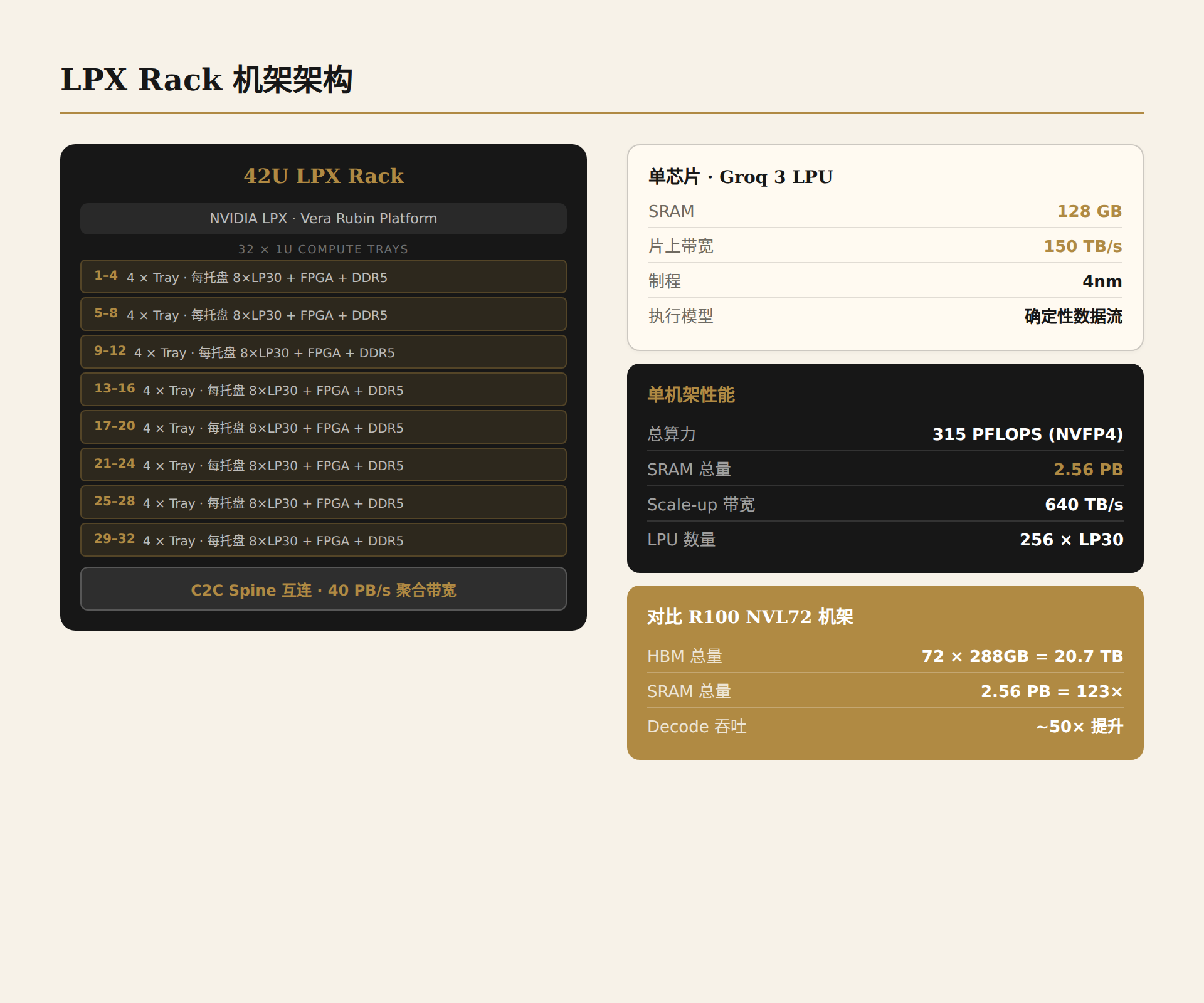
The LPX rack's core parameters are a set of memorable numbers:
| Metric | Value |
|---|---|
| LPU chip count | 256 (32 trays × 8 chips/tray) |
| Aggregated SRAM capacity | 128 GB |
| On-chip SRAM bandwidth | 40 PB/s |
| AI inference compute (FP8) | 315 PFLOPS |
| Scale-up bandwidth | 640 TB/s |
Breaking it down: 32 1U liquid-cooled compute trays, each integrating 8 LP30 chips, one host processor, and fabric extension logic. Each tray provides 4 GB SRAM, 1.2 PB/s bandwidth, 9.6 PFLOPS FP8 compute, and 20 TB/s scale-up bandwidth. These 32 trays are interconnected via LPU C2C (Chip-to-Chip) spine, forming a complete inference acceleration rack.
This architectural choice is itself a declaration: the LPU is not a GPU replacement, but a GPU complement. One LPX rack can hold all weights of a 70B FP8 model (approximately 70 GB) with room left for KV Cache. But for larger models — trillion-parameter class — it needs to work in concert with the Vera Rubin NVL72.
4.2 SRAM: The Essence of the 1800× Bandwidth Advantage
The LPX rack's most striking number is the 40 PB/s aggregated SRAM bandwidth. This figure needs unpacking.
A single LP30 chip provides 150 TB/s of on-chip SRAM bandwidth. For comparison, H100 SXM's HBM3 bandwidth is 3.35 TB/s, and B200 SXM's HBM3e bandwidth is 8 TB/s. On a per-chip basis, LPU's memory bandwidth is approximately 45× that of H100. But the more appropriate comparison is next-generation HBM4 — Samsung and SK Hynix are planning HBM4 bandwidth around 22 TB/s. Even using the most aggressive HBM4 projections, SRAM is still approximately 7× faster (single-chip dimension).
The 1800× figure comes from a different calculation: comparing the entire LPX rack's 40 PB/s aggregated bandwidth against a single GPU's HBM4 bandwidth (22 TB/s), 40,000 / 22 ≈ 1,818. This comparison is technically unfair — it pits 256 chips' aggregated bandwidth against one chip — but it precisely conveys one message: when you distribute inference across 256 SRAM-first chips, memory bandwidth ceases to be a bottleneck.
This is especially critical for the decode phase. In autoregressive inference, every generated token requires reading all model weights from memory. Take a 70B FP8 model (~70 GB weights) for example:
- H100 (3.35 TB/s): weight load time ≈ 21 ms
- B200 (8 TB/s): weight load time ≈ 8.75 ms
- Single LPU (150 TB/s): weight load time ≈ 0.47 ms
When model generation speed approaches 1000 tokens/s, the per-token budget is only 1 ms. Only SRAM can compress memory access time to below this threshold.
4.3 FPGA Scheduling Hub: The Cost and Payoff of Hardware Programmability
Each LPX compute tray includes an FPGA as a scheduling hub. Based on industry pricing estimates, a mid-to-high-end FPGA costs approximately $12,000; 32 FPGAs amounts to $384,000 — already approaching 10-15% of the LPX rack's component cost.
Why FPGA instead of ASIC? Three reasons form a logical loop:
First, scheduling strategies are evolving rapidly. Prefill/Decode disaggregation (PD disaggregation) was pioneered by UCSD Hao AI Lab, and AFD (Attention-FFN Disaggregation) extends this concept to a finer granularity. Expert routing strategies in MoE models, load balancing ratios between prefill and decode, priority scheduling in multi-tenant scenarios — all of these iterate on a quarterly cadence. If built as fixed-function ASICs, every strategy change would require a new tapeout, a 12-18 month cycle costing millions of dollars. FPGAs can be reprogrammed in weeks.
Second, load balancing requires hardware-speed response. In a 256-LPU distributed inference pipeline, token flow between chips requires precise timing synchronization. The LPU's deterministic execution model demands a programmable link scheduler to manage C2C connection timing and data routing — and FPGAs provide this flexibility.
Third, fault isolation and system resilience. In a 256-chip system, the probability of a single chip failure is non-negligible. FPGAs can remap data flows at the hardware level, routing around failed nodes without requiring software-level degradation.
But FPGA weaknesses are equally apparent: the programming barrier is extremely high. FPGA development requires specialized hardware description language (Verilog/VHDL) expertise; globally, engineers who can proficiently develop high-performance FPGA scheduling logic may number only in the thousands. This places enormous demands on NVIDIA's software ecosystem integration — how to make FPGA programmability transparent to upper-layer frameworks (Dynamo, TensorRT-LLM) will determine whether LPX can be adopted at scale.
4.4 DDR5 Backing Memory: SRAM's Reservoir
Each compute tray can access up to 256 GB DRAM through fabric extension logic, plus 128 GB on the host CPU side, for a maximum DRAM capacity of approximately 384 GB per tray. The entire rack's DDR5 total is approximately 12 TB.
The storage hierarchy design intent is clear: SRAM is the highway for hot data; DDR5 is the reservoir for warm data. During decode, active weights and current KV Cache reside in SRAM, consumed by compute units at 40 PB/s. But not all data needs this speed — cold MoE expert weights, early KV Cache from long contexts, model layers awaiting invocation — these can temporarily live in DDR5 and be DMA'd to SRAM as needed.
DDR5 also provides buffer space for model switching. When an LPX rack needs to switch from serving model A to model B, model B's weights can be loaded from DDR5 to SRAM rather than reading from network storage, dramatically reducing switchover latency.
4.5 Full Liquid Cooling and MGX Compatibility: Deployment's Practical Constraints
The LPX rack employs full liquid cooling, compatible with NVIDIA's MGX (Modular GPU Accelerator) rack architecture. This is not merely a thermal decision — it's deployment economics. Traditional air-cooled racks have a power density ceiling of approximately 30-40 kW, whereas an LPX + Vera Rubin NVL72 combined rack may exceed 100 kW. Liquid cooling pushes the power density ceiling above 150 kW, enabling data centers to deploy LPX without major facility retrofits.
MGX compatibility means LPX can share the same rack infrastructure, power distribution units (PDUs), and management network with Vera Rubin NVL72. For hyperscale data centers, this means no need to build separate facilities for LPX — it's just another cabinet next to the Vera Rubin racks.
4.6 Supply Chain: Foxconn Sole Manufacturing — Risk and Scale
Compute trays are manufactured exclusively by Foxconn, with shipments planned to begin in Q3 2026. Annual production target is 6,000 LPX racks, corresponding to 1.536 million LP30 chips. Sole-source manufacturing means single-supplier risk — any capacity fluctuation at Foxconn (whether from competing demand or geopolitical factors) directly impacts LPX delivery cadence.
LP30 chips are fabricated on Samsung's 4nm process (Groq 3 LPU public specs list Samsung 4nm, 98 billion transistors). Compared to Rubin GPU's TSMC N3P, the LPU's choice of Samsung 4nm has clear logic: an SRAM-first architecture doesn't depend on advanced process density advantages, and Samsung 4nm provides a better balance between SRAM density and cost.
V. GPU + LPU Heterogeneous Collaboration: Dynamo and AFD
5.1 AFD: Why Separate Attention and FFN
Attention-FFN Disaggregation (AFD) is the theoretical foundation of this heterogeneous architecture. It stems from a precise observation about Transformer inference: Attention and FFN have fundamentally different hardware requirements during inference.
Attention during decode is memory-capacity-intensive. KV Cache grows linearly with context length — a million-token context window may consume tens of GB of KV Cache. This data requires persistent storage, and the access pattern is irregular (attention score computation needs to access all historical tokens' KV).
FFN (Feed-Forward Network) / MoE Expert during decode is both compute-intensive and memory-bandwidth-intensive. It doesn't need to maintain cross-token state — each token passes through FFN projections independently — but it needs high-speed weight matrix reads. This is precisely SRAM's strength: fixed weights, regular access patterns, requiring extreme bandwidth.
AFD (Attention-FFN Disaggregation) extends the Prefill/Decode disaggregation concept to a finer granularity — not separation by stage, but by network layer type. The key insight: in MoE (Mixture of Experts) models, expert parallelism already requires all-to-all communication. AFD cleverly hitchhikes on this existing pattern — embedding activation transfer between Attention and FFN into the existing expert routing communication, avoiding the extra communication overhead that a pure dense Transformer would incur.
5.2 GPU Handles Prefill, LPU Handles Decode: The Logic of Division of Labor
In the Vera Rubin NVL72 + LPX heterogeneous architecture, an inference request's lifecycle is split into a relay race:
First leg: GPU processes Prefill. The user's prompt is batch-processed as one-shot matrix multiplication, highly compute-bound. Rubin GPU's Tensor Cores deliver peak FLOPS utilization in this phase — large-batch matmul is exactly GPU's home turf. After prefill completes, the generated KV Cache is passed to the next leg.
Second leg: LPU processes Decode. Entering autoregressive token generation, each token requires only small-batch matrix operations. On GPU, this phase achieves only 1-3% FLOPS utilization — compute units spend most of their time waiting for memory to return data. LPU's SRAM compresses this wait time by 45× (single-chip dimension), bringing FLOPS utilization close to peak.
Data transfer: KV Cache from GPU HBM to LPU SRAM. This is the most critical — and most fragile — link in the entire architecture. KV Cache is transferred from GPU's HBM to LPU's SRAM via PCIe/CXL or custom interconnect. Transfer latency and bandwidth directly determine the system's TTFT (Time-to-First-Token) and request switchover overhead.
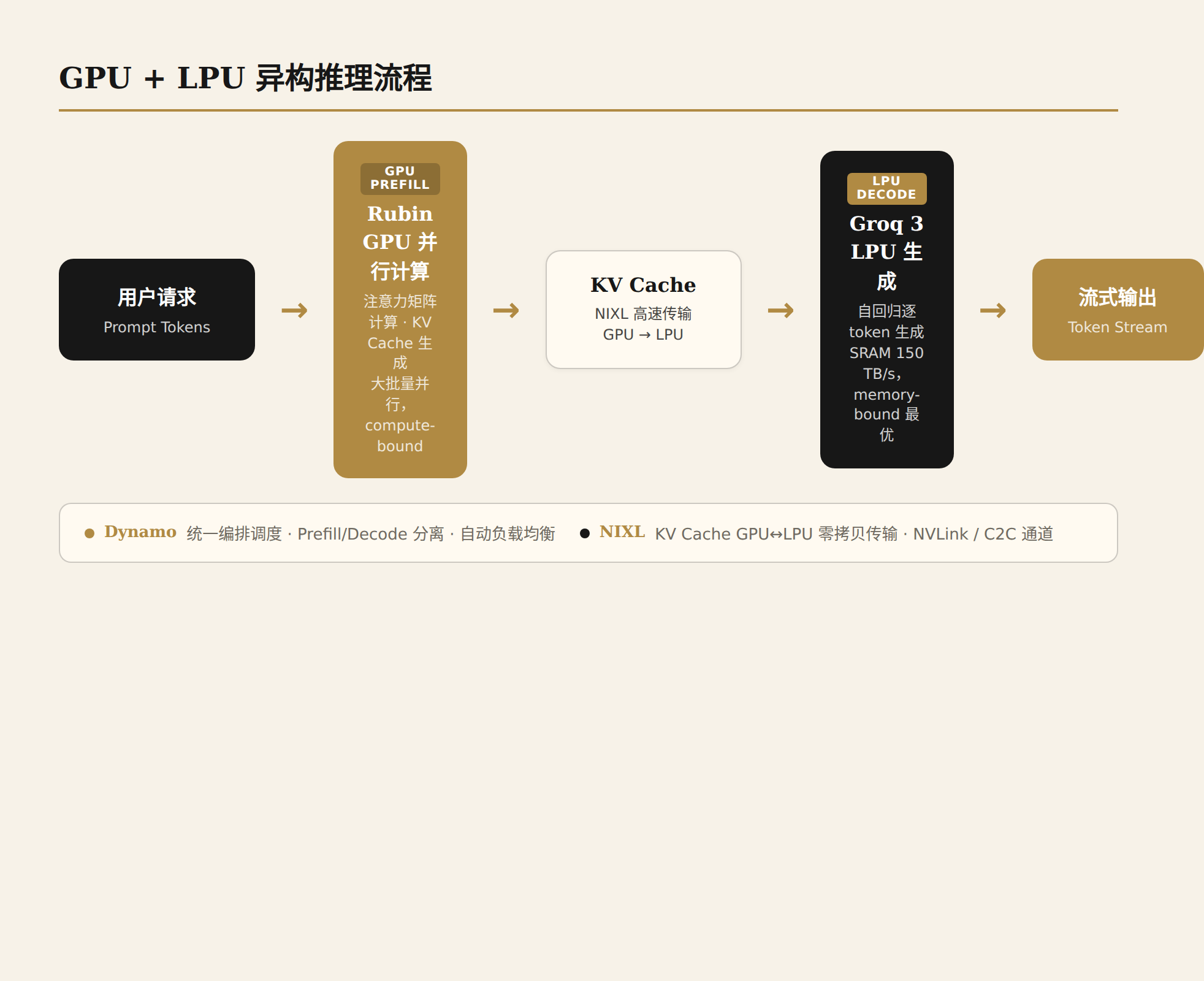
NVIDIA's own analogy is apt: Vera Rubin NVL72 is the "versatile general-purpose workhorse," responsible for training and high-throughput inference across the full pipeline; LPX is the "low-latency inference-dedicated engine," specifically accelerating latency-sensitive FFN/MoE execution within the decode loop. Together, they form a "heterogeneous inference architecture" — delivering interactive-grade low latency while maintaining AI-factory-level total throughput.
5.3 NVFusion: LPU's Technical Path into the CUDA Ecosystem
For LPU to be widely adopted, it must solve a fundamental problem: developers should not need to rewrite code for new hardware. NVFusion is NVIDIA's answer — a technical path that makes LPU transparent to developers.
Based on available information, NVFusion works similarly to how CUDA abstracts different GPU architectures: upper-layer frameworks (PyTorch, JAX, TensorRT-LLM) emit standard tensor operations, and the NVFusion runtime routes these operations to the appropriate execution device — compute-bound operations go to GPU, memory-bandwidth-bound operations go to LPU. Developers still see a unified CUDA device pool.
The key challenge for this abstraction is weight scheduling: model weights need to be dynamically allocated between GPU and LPU. In AFD mode, FFN/MoE weights reside in LPU SRAM, while Attention weights and KV Cache reside in GPU HBM. The mechanism for fast weight scheduling from GPU to LPU — how to accomplish weight loading and updating without interrupting inference service — is the core engineering challenge for the NVFusion runtime.
5.4 Software Stack: Dynamo Orchestrates the Full Pipeline
NVIDIA Dynamo is the orchestration layer for the entire heterogeneous inference architecture, managing the complete lifecycle from request receipt to token generation.
Dynamo's core capabilities include:
-
Prefill/Decode disaggregated scheduling. Dynamo splits inference requests into prefill and decode phases, routing them to GPU and LPU clusters respectively. It manages KV Cache transfer between the two and dynamically adjusts GPU-LPU allocation ratios based on real-time load.
-
Streaming Tokens. Tokens are returned to clients in streaming fashion rather than waiting for the entire sequence to be generated. In Agentic scenarios, streaming is not just a UX optimization — it's a functional requirement. Reasoning, tool calls, and code generation all need real-time token-level feedback, not a completed response.
-
Multi-Turn Agentic Harness. This is a major investment area for Dynamo in 2026. Real Agentic inference involves multi-turn structured interactions: the assistant's responses interleave thinking and tool calls, while the user (or harness) returns tool execution results in subsequent messages. Dynamo needs to precisely manage the context state of each turn — which reasoning to preserve for the next round, which to discard — a model-specific, scenario-specific strategy that cannot be generalized.
Dynamo faces concrete, real-world challenges in practice. Take the Anthropic-compatible API as an example: clients like Claude Code attach session-specific billing headers at the beginning of each request, preventing KV Cache reuse across sessions. Dynamo addresses this through the --strip-anthropic-preamble option, which strips this volatile header before tokenization. In a B200 test with a 52K-token prompt, this optimization reduced TTFT from 912ms to 168ms — approximately a 5× improvement.
5.5 NVIDIA OpenShell: A Secure Runtime for Autonomous Agents
If Agentic AI is the destination, OpenShell is the moat. It is NVIDIA's open-source secure runtime for autonomous AI agents, providing sandboxed execution environments to protect data and system security.
The core problem OpenShell solves: when an AI agent can autonomously execute shell commands, access file systems, and initiate network requests, how do you constrain risk while preserving capability? This is not purely a software problem — it involves the agent's permission model, resource isolation, audit logging, and safe degradation on failure.
OpenShell's relationship with Dynamo is complementary: Dynamo handles inference-layer orchestration (how tokens flow, how KV Cache is managed), while OpenShell handles execution-layer security (how agent tool calls are executed, where the boundaries are). When an agent issues a tool call through Dynamo's tool_call_dispatch event, actual execution occurs in OpenShell's sandbox.
5.6 Potential Issues: The Engineering Cost of Heterogeneous Execution
The GPU + LPU heterogeneous architecture's theoretical benefits are clear, but engineering practice faces a triple challenge:
Consistency across two execution models. GPUs are dynamically scheduled — warp schedulers determine instruction execution order at runtime, with variable latency. LPUs are deterministic — the compiler precisely schedules every clock cycle at compile time. The two models should produce mathematically equivalent numerical results, but minor differences may exist in floating-point precision and edge cases. Whether these differences accumulate into observable quality degradation when GPU and LPU cooperatively process different layers of the same model requires continuous verification in production environments.
Debugging complexity. When a single inference request simultaneously involves GPU (prefill + attention), LPU (FFN/MoE decode), and FPGA (scheduling) — three types of hardware — the complexity of performance tuning and fault diagnosis rises sharply. A latency spike could originate from GPU HBM access contention, LPU C2C communication congestion, or an FPGA scheduling decision. Whether current profiling tools can provide end-to-end observability in such heterogeneous environments remains an open question.
Fault isolation. In a pure-GPU system, a GPU failure means requests on that GPU need to be rerouted to other GPUs. In a GPU+LPU heterogeneous system, a component failure can cascade — if the LPU chip responsible for a certain FFN layer fails, in-progress decode requests cannot continue, while the GPU side has already generated KV Cache. The system must decide whether to drop the request or degrade to a pure-GPU path for completion. The complexity of this failover logic does not exist in pure-GPU systems.
VI. Performance Projection and Cost Analysis
6.1 "35× Inference Throughput per Megawatt" — How Is This Derived?
NVIDIA claimed at GTC 2026 that Vera Rubin + LPX achieves a "35× improvement in inference throughput per megawatt" compared to the Hopper (H100) platform. This is a layered number that needs unpacking layer by layer.
Layer 1: Blackwell vs. Hopper. According to SemiAnalysis InferenceX data, GB300 NVL72 achieved approximately 50× throughput-per-megawatt improvement and 35× per-token cost reduction in Agentic AI scenarios compared to the Hopper platform. This comes from NVFP4 low-precision inference, TensorRT-LLM optimizations, NVLink 5 bandwidth improvements, and the NVL72 rack-level full-mesh interconnect architecture.
Layer 2: Rubin vs. Blackwell. NVIDIA officially claims Vera Rubin NVL72 achieved "cost per million tokens reduced to 1/10" and "complete AI training with 1/4 the GPUs" compared to Blackwell. This implies Rubin itself delivers approximately 10× inference efficiency improvement over Blackwell.
Layer 3: Rubin + LPX vs. Rubin alone. LPX's addition further accelerates the decode phase. In AFD mode, LPU takes on all FFN/MoE decode workload, freeing GPU for prefill and attention. The combined effect depends on the workload's prefill/decode ratio — for long-output, multi-turn Agentic scenarios (decode ratio > 80%), LPX's marginal contribution is greatest.
The 35× figure comes from the approximately 10× improvement from Hopper → Rubin, compounded by an additional 3-4× from LPX in decode-heavy scenarios. Prerequisites are: MoE model architecture (AFD only works with MoE), long-context + long-output Agentic workload, and a complete GPU+LPU heterogeneous deployment software stack (Dynamo + NVFusion) ready.
6.2 Data Inconsistencies: 307 vs 315 PFLOPS, 38.4 vs 40 PB/s
In LPX's public materials, there are two sets of inconsistent data:
PFLOPS: NVIDIA's official technical blog gives the LPX rack compute as 315 PFLOPS (32 trays × 9.6 PFLOPS/tray = 307.2 PFLOPS). The difference between 315 and 307.2 (approximately 2.5%) may come from: rounding of per-tray compute, inclusion of auxiliary compute from scheduling FPGAs, or different NVIDIA naming conventions across scenarios (peak vs. sustained). This falls within normal engineering tolerance and does not affect system-level assessment.
Bandwidth: The difference between 40 PB/s and 38.4 PB/s (256 × 150 TB/s = 38,400 TB/s = 38.4 PB/s) is similar. 40 PB/s may be NVIDIA's rounded-up nominal value, while 38.4 PB/s is the strict multiplication result. The approximately 4% difference is understandable in the context of aggregated bandwidth.
These inconsistencies are not fatal, but they serve as a reminder: there is a systematic gap between NVIDIA's marketing launch data and technical specifications — the former tends toward rounding up and idealization, while the latter is closer to engineering reality. In cost analysis, the lower numbers should be used to maintain conservatism.
6.3 Token Cost Curve: Blackwell → Rubin → Rubin + LPX
Based on public data, the token cost projection is as follows:
Blackwell Generation (2025-2026): H100's cost per million tokens is approximately $0.26 (70B FP8, on-demand). B200 through FP8 quantization and large-batch optimization drops to approximately $0.30 (seemingly higher, but dramatically increased throughput means actual per-token cost can drop to approximately $0.16 in optimized configurations). GB300 NVL72's arrival brings scale effects — NVIDIA claims a 35× cost advantage over Hopper.
Rubin Generation (2026-2027): NVIDIA officially claims Vera Rubin NVL72 achieved a 10× cost reduction over Blackwell. If GB300 NVL72's token cost is 1/35 of Hopper's, then Vera Rubin's token cost is approximately 1/350 of Hopper's. However, this figure needs validation in real workloads — MoE model expert routing overhead, long-context KV Cache management, and resource contention in multi-tenant scenarios can all erode theoretical advantages.
Rubin + LPX: LPX's addition primarily reduces cost further in the decode phase. For decode-heavy Agentic workloads, LPU's SRAM bandwidth advantage means higher token output per watt. Rough estimate: compared to a pure Rubin solution, LPX can reduce per-token cost in the decode phase by an additional 2-3× (depending on decode ratio).
NVIDIA's recommended GPU-to-LPU deployment ratio is 3:1, meaning approximately 25% of inference compute budget goes to LPU. This ratio corresponds to workloads primarily featuring dense LLM inference (7B-70B). For large MoE models (trillion-parameter class), LPU's share may need to be higher — because more FFN/MoE expert layers need LPU bandwidth for acceleration.
6.4 Rubin Shipment Share Revised Down: The Signal from 29% → 22%
SemiAnalysis reports that Rubin's shipment share was revised down from the previously expected 29% to 22%. The implications of this adjustment are multi-layered:
Optimistic reading: Blackwell (B200/B300/GB300) demand exceeded expectations, with customers purchasing large quantities of Blackwell systems before Rubin matures. This means AI inference market demand is accelerating, and existing hardware digestion capacity is stronger than expected.
Cautious reading: Rubin's volume ramp encountered unexpected difficulties — perhaps HBM4 supply chain bottlenecks, insufficient liquid cooling infrastructure, or software stack immaturity. LPX, as part of the Rubin platform, has its delivery cadence directly affected by Rubin's overall progress. If Rubin is delayed, LPX is also delayed.
6.5 Practical Deployment Constraints
LPX's theoretical performance is impressive, but practical deployment faces three constraints:
HBM4 supply chain. Vera Rubin GPU needs HBM4, and HBM4 production ramp is slower than expected. Samsung and SK Hynix's HBM4 production lines remain in early stages in 2026. If GPU's HBM4 supply is insufficient, even if LPX racks are ready, the entire heterogeneous system cannot run at full capacity — because GPUs handle prefill and attention, and without GPUs there is no complete inference pipeline.
Liquid cooling engineering. The LPX rack's full liquid cooling design requires data centers to have corresponding liquid cooling infrastructure. The proportion of data centers globally that can support 100 kW+ cabinet density remains low (estimated < 15%). Liquid cooling's capex investment and operational complexity create deployment barriers.
FPGA programming complexity. As discussed earlier, FPGA scheduling logic development and maintenance requires scarce specialized talent. If NVIDIA cannot sufficiently abstract FPGA programmability (through toolchains and automation), LPX's software adaptation cost will become an obstacle to large-scale deployment.
6.6 ROI Comparison with Pure-GPU Solutions
The ultimate question: keep stacking GPUs (B300/GB300), or invest in the GPU+LPU heterogeneous solution?
The pure-GPU approach has the advantage of simplicity and flexibility. The same GPU cluster can run training, inference, fine-tuning, multimodal — no workload is excluded. Blackwell Ultra (B300) and GB300 NVL72 have already achieved significant efficiency improvements in Agentic AI scenarios.
The GPU+LPU approach has the advantage of extreme efficiency in the decode phase. For decode-heavy workloads (> 80% decode), LPU's SRAM bandwidth can improve per-watt token output by an order of magnitude. But the tradeoff is architectural complexity (two types of hardware, heterogeneous scheduling, FPGA programming) and workload restrictions (LPX can only run LLM decode, not training or prefill).
The ROI tipping point depends on: whether your inference workload is sufficiently decode-heavy, whether it primarily uses MoE models, and whether you need 1000+ tokens/s interactive speed. If the answer to all three is "yes," the GPU+LPU investment payback period may turn positive within 12-18 months. If workloads are diverse, model sizes vary widely, or batch-oriented inference dominates, the pure-GPU approach may still be superior in total cost of ownership.
A pragmatic deployment strategy is NVIDIA's recommended 3:1 mix ratio — 75% GPU, 25% LPU. This provides dedicated acceleration for the most latency-sensitive decode workloads without sacrificing flexibility. As LPX's software ecosystem matures and pricing becomes public, this ratio can be dynamically adjusted based on actual ROI data.
VII. Supply Chain and Market Landscape
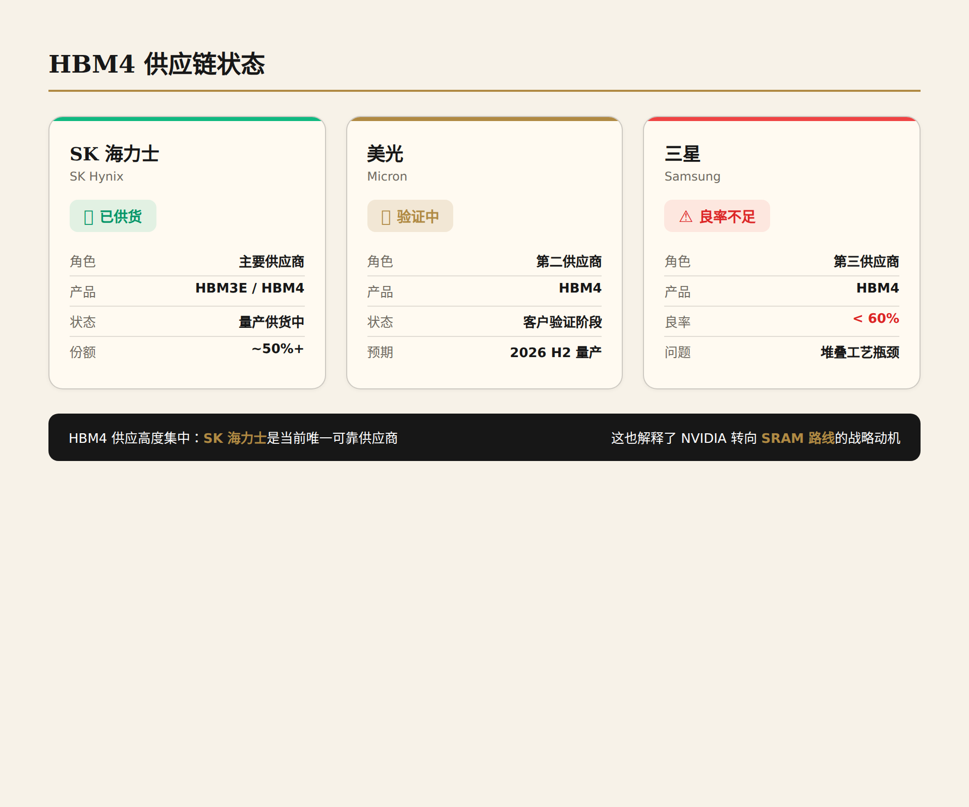
HBM4: The First Bottleneck Choking Rubin
In the second half of 2025, NVIDIA aggressively raised HBM4's per-pin data rate target from 8 Gbps to 11.7 Gbps — a number approaching physical limits. All three suppliers were forced to re-qualify, and volume production timelines were disrupted.
As of May 2026, the situation shows a clear tier separation:
- SK Hynix has progressed fastest, supplying NVIDIA in Q1 2026 with smooth qualification, essentially locking in the position of primary HBM4 supplier for the first batch.
- Micron has entered high-volume production but lags behind in qualification pace.
- Samsung is the biggest variable: internal qualification has passed and customer samples have been provided, but DRAM yield remains below 60% — a significant gap from the 70% threshold for volume production. If Samsung cannot pull yield above the qualifying line by end of Q2, NVIDIA's total HBM4 supply will be compressed by approximately one-third.
This shortfall is forcing NVIDIA into an unwelcome compromise: considering accepting sub-max-speed HBM4 variants. This means some Rubin GPUs may ship with memory bandwidth below design spec, with corresponding performance penalties. For a platform whose core selling point is "token cost reduced to one-tenth of Blackwell," any reduction in memory bandwidth directly undermines the economic model.
All three suppliers are expected to complete full qualification by end of Q2 2026. If timelines slip again, Rubin's Q3 volume shipment plan faces material risk.
Rubin Shipment Share Revised Down: From 29% to 22%
The shipment share revision from 29% to 22% may look like a 7-percentage-point tweak on the surface, but the actual impact is far greater:
- Absolute numbers: Based on NVIDIA FY2027 data center revenue benchmarks, 7 percentage points corresponds to approximately $5-7 billion in deferred revenue recognition.
- Customer confidence: Microsoft, Google, Amazon, Meta, and Oracle — the five first-wave customers — have signed delivery windows. The revision means some customers will have to extend their Blackwell run cycles or pivot to ASIC solutions to fill the gap.
- Opportunity cost: The delayed Rubin shipment window is exactly when Google TPU v6e and Amazon Trainium3 are accelerating their penetration. Every week of delay pushes potential customers toward in-house ASICs.
The root cause of the revision is not just HBM4 qualification. Liquid cooling engineering complexity is another underappreciated constraint — the Vera Rubin NVL72 rack consumes over 120 kW, placing unprecedented demands on data center liquid cooling infrastructure. Some customers' data center retrofit progress cannot keep pace with chip delivery, creating the awkward situation of "chips arrived but the facility isn't ready."
SOCAMM2: A Memory Revolution on the CPU Side
While GPU-side HBM4 grabs all the attention, NVIDIA is quietly advancing a new standard that could reshape AI server memory architecture: SOCAMM2.
SOCAMM2 (Small Outline Compute Accelerated Memory Module 2) is led by NVIDIA and co-developed with Samsung, SK Hynix, and Micron. Core specs:
- Based on LPDDR5X, 128-bit bus width, 8533 MT/s
- 128 GB capacity per module
- Cost approximately 1/4 of HBM
- Replaceable and expandable — something unimaginable in the HBM world
SOCAMM2's positioning is not to replace HBM, but to provide large-scale data caching on the CPU side. The Vera CPU is equipped with 256 GB of SOCAMM2, providing ample low-cost memory space for data preprocessing, model loading, and KV Cache management.
This is a clever tiered strategy: use HBM to serve the GPU compute cores' bandwidth hunger, use SOCAMM2 to fill the CPU-side capacity gap, with NVLink-C2C interconnect between the two. The cost structure is thereby optimized — implementing 256 GB entirely in HBM would cost close to $8,000 for CPU-side memory alone; switching to SOCAMM2 brings cost below $2,000.
Foxconn Capacity Expansion: From 1000 to 2000
Foxconn is executing an aggressive capacity expansion plan: increasing AI server rack weekly production from 1,000 to 2,000 units. This is not merely linear production line expansion — it requires:
- Liquid cooling assembly lines scaling proportionally; each Vera Rubin NVL72 rack requires custom cold plates and tubing installation
- Testing capacity increasing in parallel; the 72-GPU + 36-CPU interconnect test takes over 48 hours per unit
- Supply chain coordination: TSMC N3P production line Rubin chip output, Samsung 4nm LPU chip output, and HBM4 supply — all three lines must be aligned to weekly delivery cadence
Foxconn also holds the exclusive manufacturing contract for Groq 3 LPX compute trays and is responsible for the majority share of rack assembly. 2026 projected delivery is 6,000 LPX racks, with an additional 10,000 planned for 2027. This means Foxconn's role in AI server manufacturing is evolving from "assembly plant" to "system-level integrator."
Domestic Challenger: Yuanchuan Micro's LPU+
Beyond NVIDIA + Groq, China's LPU track is seeing its first significant entrant: Yuanchuan Micro.
In April 2026, Yuanchuan Micro closed a nine-figure RMB angel round. Investors included Oriental Jiafu, Yuanhe Origin (which invested in Cambricon a decade ago), and Fengrui Capital. Founder Yang Bin has 22 years of Huawei wireless baseband experience — a background worth noting: baseband processors are essentially high-throughput, deterministic signal processing chips, and their design philosophy naturally aligns with the LPU's deterministic execution model.
Yuanchuan Micro's LPU+ chip claims native support for large language models, MoE architectures, and multimodal inference. Unlike Groq's inference-acceleration-first approach, LPU+ attempts to provide hardware-level support for MoE's sparse expert routing at the architecture level, potentially yielding higher efficiency advantages on domestic MoE models like DeepSeek and Qwen.
But practical challenges are equally apparent: Groq has NVIDIA's software ecosystem (NVFusion, Dynamo) and world-class customer validation; Yuanchuan Micro must build its software stack from scratch and find profit margins in China's intensely price-competitive compute market. TSMC CoWoS capacity allocated to domestic customers remains limited, and advanced packaging may become another bottleneck.
Inference Market Landscape: From GPU Monopoly to Dual-Track
The death of CPX and the rise of LPU are changing AI infrastructure procurement logic.
Previously, inference and training shared the same GPU infrastructure, differing only in batch size and precision settings. NVIDIA's monopoly was unchallenged. But LPU's emergence means inference for the first time has economic justification for dedicated hardware.
For hyperscale cloud providers, a new procurement decision tree is taking shape:
- Training: Continue using GPUs (Rubin NVL72); HBM's high bandwidth is irreplaceable
- Prefill (first-token generation): GPU's compute advantage remains strong, especially for large-batch scenarios
- Decode (token-by-token decoding): LPU's SRAM architecture and deterministic execution provide 10×+ throughput advantage
NVIDIA is transitioning from a "GPU monopolist" to a "GPU+LPU dual-track supplier." This transition presents entirely new challenges for NVIDIA's own organization, pricing strategy, and customer relationships. Jon Peddie's assessment is spot-on: "LPU doesn't compete with GPU; it completes it."
And for latecomers to the inference market — Cerebras ($95B market cap IPO), SambaNova, and Yuanchuan Micro — NVIDIA's self-disruption is more favorable than stubborn defense: it validates the market existence of dedicated inference hardware, educates customers, and opens procurement budget category windows.
VIII. Looking Ahead: The Ultimate Convergence of Feynman and CPO (2028+)
One Chip, Two Souls
If Vera Rubin is NVIDIA's first step in learning how to make GPU and LPU coexist, then the Feynman architecture is the ultimate answer: not two chips collaborating in the same rack, but both baked into the same chip.
Feynman is based on TSMC's A16 process — 1.6nm, the world's first sub-1nm AI chip. GAA (Gate-All-Around) transistors provide more precise current control than FinFET, and SPR (Super Power Rail) backside power delivery moves the power network from the transistor front to the back, freeing up valuable routing resources.
These may sound like standard process node advances. But A16's true significance for Feynman lies in: the front-side space freed by backside power delivery provides the physical conditions for 3D stacking.
SoIC Hybrid Bonding: LPU Stacked on Top of GPU
Feynman's core architectural innovation is SoIC (System on Integrated Chips) hybrid bonding — stacking Groq LPU compute units directly on top of the GPU main die.
This is not simple chip packaging; it is the vertical integration of two fundamentally different computing architectures at the silicon level:
- Bottom layer (GPU die): responsible for training and Prefill; high-bandwidth compute; accesses model weights through HBM
- Top layer (LPU die): responsible for Decode; abundant SRAM provides deterministic high-speed inference; no HBM dependency
- Inter-layer interconnect: SoIC hybrid bonding achieves μm-level interconnect density; inter-layer bandwidth far exceeds any board-level interconnect
Vertical stacking solves the latency and bandwidth bottlenecks of connecting GPU and LPU through FPGA and NVLink in the Vera Rubin architecture. Physical distance shrinks from "cross-board within a rack" to "μm-level cross-layer within the same chip," dropping latency by several orders of magnitude.
Theoretical inference performance reaches 50 PFLOPS — a 5× improvement over Blackwell. Note what this number means: it is not performance gain from process scaling alone, but the result of an architectural paradigm shift.
CPO Silicon Photonics: The Terminator of Copper Cables
The other pillar of the Feynman architecture is CPO (Co-Packaged Optics).
When single-chip power breaks through 2000W and single-rack power exceeds 150 kW, copper cable interconnect's physical limits become an unavoidable bottleneck. Signal attenuation, power consumption, volume, heat dissipation — copper is approaching physical boundaries on every dimension.
CPO replaces copper cables with silicon photonics technology:
- 60% reduction in transmission loss: optical signal attenuation in silicon waveguides is far lower than electrical signal attenuation in copper wires
- 70%+ reduction in energy consumption: no signal amplification and equalization circuits needed
- Increased bandwidth density: a single optical fiber can carry multiple wavelengths, with equivalent bandwidth far exceeding copper cable
- Physical volume reduction: optical fibers replacing copper cables dramatically frees up in-rack wiring space
CPO's role in Feynman is not just inter-GPU connectivity, but the external expansion interconnect between GPU+LPU vertically stacked chips. When a single Feynman chip contains complete inference capability for both GPU and LPU, cooperative communication between multiple Feynman chips requires CPO-level bandwidth and energy efficiency.
Diamond Cooling: The Practical Challenge of 2000W
What does single-chip power breaking through 2000W mean?
Current state-of-the-art direct-to-chip liquid cooling (DLC) solutions are approaching their practical comfort zone at around 1000W. 2000W pushes thermal management into uncharted territory. Feynman introduces a diamond cooling solution — leveraging synthetic diamond's extremely high thermal conductivity (~2000 W/m·K, 5× that of copper) as the thermal interface material between chip and cold plate.
Diamond cooling has been validated as feasible in laboratory settings, but cost and reliability in mass production remain question marks. Synthetic diamond costs are declining rapidly but remain an order of magnitude higher than traditional thermal interface materials (TIMs). NVIDIA needs to find the balance between cooling performance and mass production cost.
Intel's Involvement: EMIB Packaging
An easily overlooked detail: NVIDIA's $5 billion strategic investment in Intel is bearing fruit. Intel's EMIB (Embedded Multi-die Interconnect Bridge) packaging technology will participate in approximately 25% of Feynman's packaging tasks.
EMIB is a high-density silicon bridging technology that embeds small silicon chips within an organic package substrate, providing high-density interconnect between dies. Compared to TSMC's CoWoS, EMIB has cost advantages in medium interconnect density scenarios and doesn't require a silicon interposer for the entire package.
NVIDIA having Intel handle approximately one-quarter of packaging tasks serves both as capacity diversification (reducing single-source dependency on TSMC CoWoS capacity) and geopolitical risk management. But it also means Feynman's packaging yield will be simultaneously affected by both TSMC's and Intel's process capabilities — quality control complexity rises significantly.
Engineering Challenge Checklist
Feynman's 2028 deployment faces three engineering challenges:
1. Thermal density. 3D stacking places two heat sources on top of each other; local heat flux density may exceed 100 W/cm². Even with diamond cooling, how to conduct heat from the LPU layer through the GPU layer to the cold plate is a problem not yet fully solved.
2. CUDA compatibility. LPU uses a deterministic execution model, fundamentally different from traditional GPU's SIMT architecture. The NVFusion software layer needs to ensure existing CUDA programs can transparently leverage LPU resources without requiring developers to rewrite code. The completeness of this "transparency" will directly determine Feynman's ecosystem moat.
3. Yield. 3D stacking means two dies' yields multiply. If GPU die yield is 80% and LPU die yield is 90%, stacked overall yield is only 72%. In the early stages of A16 process, individual die yields may be far below 80%, making stacked effective output potentially alarmingly low.
IX. Summary and Judgment
The Deeper Meaning of CPX's Death
In September 2025, NVIDIA launched Rubin CPX — a GPU using GDDR7 memory, specifically designed for large-scale context inference. Five months later, CPX disappeared from the roadmap, replaced by Groq 3 LPU.
On the surface, this is a product line adjustment. At a deeper level, this is NVIDIA formally acknowledging for the first time: inference requires dedicated architecture, not a "down-specced training GPU."
CPX's design philosophy was traditional: use cheaper memory (GDDR7 replacing HBM) to reduce inference costs. But it was still a GPU, still constrained by the SIMT architecture's parallel scheduling model, still facing memory bandwidth bottlenecks in the decode phase.
LPU solves the problem in a fundamentally different way: abandon HBM, use abundant on-chip SRAM for deterministic memory access; abandon parallel scheduling, use deterministic execution to eliminate scheduling overhead. This is not "a better GPU" — it is "something else entirely."
NVIDIA spent $200 billion acquiring Groq to gain this cognitive transformation — a steep price. But compared to continuing to invest engineering resources in the wrong direction with the CPX product line, this tuition was worth paying.
LPU Is a Complement, Not a Replacement
An emerging market consensus is: LPU will not replace GPU, but will form functional complementarity with it.
- GPU excels at: training, Prefill, high-throughput compute, flexible model adaptation
- LPU excels at: Decode, low-latency inference, deterministic throughput, long-context processing
This complementary relationship changes AI infrastructure procurement logic. Previously, CTO/VP-level compute purchasing decisions were "how many GPUs to buy." Now, the decision has become "how many GPUs for the training cluster, and what GPU+LPU combination ratio for the inference cluster."
NVIDIA's Dynamo software stack is automating this combination: GPU handles Prefill (attention computation), LPU focuses on Decode (token-by-token generation), with the AFD (Attention-FFN Disaggregation) mechanism dynamically scheduling workloads between the two. From the user's perspective, it's a unified inference service; from the hardware perspective, it's two fundamentally different chips collaborating.
Short-Term Risks (Next 6 Months)
HBM4 supply chain is the biggest short-term risk. If Samsung yield cannot break through the 70% threshold by end of Q2, NVIDIA will be forced to accept sub-max-speed HBM4, and Rubin's actual performance and cost competitiveness will be discounted.
FPGA cost is an underestimated hidden cost. Each Groq 3 LPX rack comes standard with 32 FPGAs at $12,000 each, resulting in $384,000 in FPGA hardware cost per rack. In a rack priced in the millions of dollars, this proportion may not seem large, but it means a portion of LPX's cost structure cannot be amortized through chip volume production — FPGAs are programmable devices with relatively fixed per-unit costs.
Software maturity is the third short-term risk. NVFusion and Dynamo are both new software stacks that need time to mature in production environments. Groq was acquired only four months before productization was completed, described as "the fastest productization in semiconductor history" — speed is good, but speed also means insufficient real-world validation.
Medium-Term Watchpoints (2026 Q3-Q4)
Actual performance data from the first LPX deployments in Q3 2026 will be the key observation window. 6,000 LPX racks will generate the first batch of real-world benchmark data:
- Gap between actual token throughput and theoretical values
- Latency performance of LPU-GPU collaboration (AFD)
- Long-term stability of liquid cooling systems
- Efficiency differences across model architectures (dense vs. MoE)
This data will determine whether LPX proceeds to "expanded deployment" or "needs significant adjustments." For CTOs evaluating inference infrastructure, Q3 data will be more persuasive than any product presentation.
Long-Term Bets (2028+)
Can Feynman's 3D stacking truly solve the GPU+LPU physical distance problem?
This is NVIDIA's ultimate bet in AI inference. If SoIC hybrid bonding and CPO silicon photonics can land on schedule in 2028, NVIDIA will possess a complete solution covering both training and inference within a single chip, completely eliminating interconnect latency between GPU and LPU.
But this bet carries equally extreme risks:
- A16 process volume production yield is unknown
- 3D stacking escalates thermal challenges from "planar" to "volumetric"
- Diamond cooling mass production cost remains unknown
- Mixed packaging quality control between Intel EMIB and TSMC SoIC
If Feynman succeeds, NVIDIA will establish a generation's worth of technological leadership in inference. If it fails — or is delayed to 2029-2030 — competitors (Google TPU, Cerebras, and even domestic players like Yuanchuan Micro) will gain a 2-3 year window to build their own inference ecosystems.
Final Judgment
NVIDIA is doing something difficult but right: using acquisition and self-disruption to avoid being disrupted. The $200 billion Groq acquisition is not a defensive move, but an offensive architectural restructuring — elevating inference from a "GPU downgrade task" to a core business requiring dedicated hardware.
CPX's death is not failure; it's learning. LPU's rise is not expediency; it's direction. Feynman is not a vision; it's a bet.
For observers, Q3 2026 will be the first real data point to validate all of this. Until then, all the 50 PFLOPS and 2000W figures remain numbers on paper.
Appendices
Appendix A: Vera Rubin NVL72 Full Specification Table
| Parameter | Specification |
|---|---|
| GPU | |
| Chip name | Rubin GPU |
| Process | TSMC 3nm (N3P) |
| Transistor count | 336 billion |
| Memory | 288GB HBM4 |
| Memory bandwidth | 22 TB/s |
| Interconnect | NVLink 6, 3.6 TB/s bidirectional per GPU |
| Inference performance (FP4) | 50 PFLOPS |
| Training performance | 35 PFLOPS |
| CPU | |
| Chip name | Vera CPU |
| Architecture | 88-core Olympus (Armv9.2) |
| Interconnect | NVLink-C2C |
| Memory | 256GB SOCAMM2 LPDDR5X |
| System | |
| GPU count | 72 Rubin GPUs |
| CPU count | 36 Vera CPUs |
| System interconnect | 72 GPU non-blocking NVLink communication |
| Token cost | 1/10 of Blackwell |
| 2026 projected shipments | ~12,000 NVL72 units |
| Single rack price | Approximately $180 million |
Appendix B: Groq 3 LPU / LPX Rack Specification Table
| Parameter | Specification |
|---|---|
| LPU Chip | |
| Chip name | Groq 3 LPU |
| Process | Samsung 4nm |
| Transistor count | 98 billion |
| On-chip SRAM | 500MB |
| External memory | No HBM |
| Chip bandwidth | 150 TB/s (7× HBM4) |
| FP8 compute | 1.2 PFLOPS |
| First-token latency | < 0.1s |
| C2C links | 96 × 112 Gbps |
| LPX Rack | |
| FPGA count | 32 per rack (1 per compute tray) |
| Single FPGA value | ~$12,000 |
| Single rack FPGA total cost | ~$384,000 |
| Manufacturing | Foxconn exclusive (compute trays) |
| Delivery Plan | |
| 2026 shipments | 6,000 LPX racks |
| 2027 shipments | 10,000 LPX racks |
| 2026 chip shipments | 1.5 million (LP30+LP35) |
| 2027 chip shipments | 2.5 million |
| 2027 next-gen | LP40 (NVLink support) |
Appendix C: NVLink Bandwidth Evolution Table
| Generation | NVLink Version | Bidirectional Bandwidth per GPU | Corresponding Platform | Timeline |
|---|---|---|---|---|
| NVLink 4 | 4.0 | 900 GB/s | Hopper H100 | 2024 |
| NVLink 5 | 5.0 | 1.8 TB/s | Blackwell B200 | 2025 |
| NVLink 6 | 6.0 | 3.6 TB/s | Vera Rubin NVL72 | 2026 H2 |
| NVLink 7 (expected) | 7.0 | ~7.2 TB/s (estimated) | Feynman | 2028+ |
Note: NVLink bandwidth roughly doubles each generation. NVLink 7 is not yet officially confirmed; estimated based on the doubling trend from NVLink 6.
Appendix D: Key Terminology Glossary
| Term | Full Name | Description |
|---|---|---|
| LPU | Language Processing Unit | Dedicated language inference chip using SRAM instead of HBM; deterministic execution model; optimized for decode scenarios |
| AFD | Attention-FFN Disaggregation | Attention-feed-forward disaggregation; GPU handles Prefill (attention computation), LPU handles Decode (FFN computation) |
| CPO | Co-Packaged Optics | Co-packaged optics; integrates silicon photonic devices with compute chips, replacing copper cable interconnects |
| SOCAMM2 | Small Outline Compute Accelerated Memory Module 2 | LPDDR5X-based modular memory standard; cost approximately 1/4 of HBM; designed for large-scale CPU-side caching |
| NVFusion | NVIDIA Fusion | NVIDIA software middleware enabling LPU to seamlessly integrate into the CUDA ecosystem; transparent to developers |
| SPR | Super Power Rail | TSMC A16 process backside power delivery technology; moves power network from transistor front to back |
| SoIC | System on Integrated Chips | TSMC 3D stacking technology; achieves μm-level high-density inter-chip interconnect through hybrid bonding |
| EMIB | Embedded Multi-die Interconnect Bridge | Intel packaging technology; embeds silicon bridges in organic substrates for high-density inter-die interconnect |
| GAA | Gate-All-Around | Gate-All-Around transistor architecture; adopted in A16 process; provides more precise current control than FinFET |
| Dynamo | NVIDIA Dynamo | NVIDIA inference orchestration framework; supports multi-turn Agentic reasoning, Streaming Tokens + Tools |
| NVL | NVLink | NVIDIA GPU interconnect architecture; NVL72 indicates 72 GPUs fully interconnected via NVLink |
| CPX | Context Processing eXtension | Cancelled Rubin inference GPU design; used GDDR7 memory; replaced by LPU in 2026-03 |
| DLC | Direct Liquid Cooling | Direct-to-chip liquid cooling; routes coolant directly to the chip surface for heat dissipation |
| CoWoS | Chip on Wafer on Substrate | TSMC advanced packaging technology; 2.5D silicon interposer enables high-density multi-chip integration |
| PD Disaggregation | Prefill-Decode Disaggregation | Separates inference Prefill and Decode phases across different hardware; pioneered by UCSD Hao AI Lab |