The Hook: Why Were NVL72's Copper Cables Sentenced to Death Within Two Years?
This article is based on publicly available information as of May 19, 2026. Data source notation: [Official] = NVIDIA published; [Estimated] = calculated from public parameters; [Third-party] = media/research reports. NVIDIA's Q1 earnings tomorrow may bring corrections.
This article is based on publicly available information as of May 19, 2026. Data source notation: [Official] = NVIDIA published; [Estimated] = calculated from public parameters; [Third-party] = media/research reports. NVIDIA's Q1 earnings tomorrow may bring corrections.
The Hook: Why Were NVL72's Copper Cables Sentenced to Death Within Two Years?
In March 2024, NVIDIA launched the GB200 NVL72. Jensen Huang called it "turning 72 GPUs into one giant GPU." The rack contained 5,000 copper cables, weighing 1.4 tons in total, with 130 TB/s bidirectional bandwidth. At 200G SerDes, those 5,000 copper cables wove a massive inter-GPU communication spine.
But just two years later, Rubin Ultra NVL576 abandoned copper cables entirely, switching to a 78-layer PCB orthogonal backplane. The Cable Tray — that copper spine Jensen Huang proudly showcased — completely disappeared.
This isn't just "changing cables." Behind it lies an irreconcilable tension between the exponential growth in AI compute demand and the physical limits of copper. From NVL72 to NVL576, physical form factor, interconnect topology, chip architecture, thermal management, and the software stack were all simultaneously restructured. Understanding this trajectory is essential to grasping why NVIDIA killed Rubin CPX, acquired Groq, skipped NVL144 — and why the "30x inference improvement" is actually conservative.
This article answers these questions:
- From NVL72 to NVL576, what actually changed in the physical form factor? And why did it have to change?
- From NVLink 5 to NVLink 6, what are the fundamental changes in interconnect architecture?
- How do GPU, CPU, and LPU divide responsibilities within a supernode? What are the engineering constraints?
- How does the software stack unlock hardware performance? Why is Dynamo the "OS of the AI factory"?
- How do real-world benchmarks evolve? From H100 to GB300 NVL72, how many times faster is inference, really?
- Why were copper cables eliminated? What does the orthogonal backplane solve, and what new problems does it introduce?
- Why was NVL144 skipped? What does this mean for the product cadence?
1. Four Generations of Supernodes at a Glance
| Dimension | GB200 NVL72 | GB300 NVL72 | Vera Rubin NVL72 | Rubin Ultra NVL576 |
|---|---|---|---|---|
| Launch | 2024.03 | 2025.07 | 2026.01/03 | 2027H2 (planned) |
| GPU | Blackwell 2-Die | Blackwell Ultra 2-Die | Rubin 2-Die N3P | Rubin Ultra 2+2 modular N3P |
| GPU Die Count | 72 | 72 | 72 | 576 |
| CPU | Grace 72-core | Grace 72-core | Vera 88-core Arm v9.2 | Vera (same) |
| HBM | 192GB HBM3e | 288GB HBM3e | 288GB HBM4 | 1TB HBM4e |
| HBM Bandwidth/Package | 8 TB/s | 8 TB/s | 22 TB/s | ~32 TB/s [Estimated] |
| FP4 Inference | 720 PFLOPS | 1,080 PFLOPS | 3.6 EFLOPS | 15 EFLOPS |
| FP8 Training | ~360 PFLOPS [Estimated] | ~540 PFLOPS [Estimated] | 2.5 EFLOPS | 5 EFLOPS |
| NVLink | 5th, 1.8TB/s/GPU | 5th, 1.8TB/s | 6th, 3.6TB/s | 6th, 3.6TB/s |
| Rack NVLink | 130 TB/s | 130 TB/s | 260 TB/s | 1.5 PB/s |
| Interconnect Medium | Copper Cable Tray | Copper Cable Tray | Cable-less modular (copper traces) | PCB orthogonal backplane |
| Per-GPU Power | ~1000W | ~1400W | ~2000W | ~2000W+ [Estimated] |
| Rack Power | ~120kW | ~140-150kW | ~200kW | ~400+kW [Estimated] |
| Scale-Out | CX-7 400Gb/s | CX-8 800Gb/s | CX-9 1.6Tb/s+BF4 | CX-9+CPO |
| Inference Software Stack | TensorRT-LLM | TensorRT-LLM+Dynamo early | Dynamo 1.0 | Dynamo + AFD |
| Status | In production | In production | In validation | Not yet in production |
Note: Late March 2026 supply chain correction — Rubin Ultra was adjusted from "single-package 4-Die" to "2-Die base unit + PCB/CoWoP 2+2 stitching." Total compute remains unchanged, but packaging complexity decreases while system-level PCB complexity increases. [Third-party]
Three Key Numbers to Read This Table
The "576" in NVL576 refers to Die count, not package count. Rubin Ultra has 4 Dies per package (actually 2+2 modular stitching), 144 packages × 4 = 576. [Official] This reflects a philosophical shift in NVIDIA's design: no longer pursuing极致 per-Die performance, but instead scaling compute through multi-Die packaging at the system level.
Compute grows 20x while Die count grows 8x. From GB200 to Rubin Ultra, FP4 inference goes from 720 → 15,000 PFLOPS (~20x), but Die count only grows 8x (72 → 576), meaning per-Die compute actually only grew ~2.6x. The driver of system-level compute growth is shifting from "faster chips" to "bigger systems."
Power grows 3.3x while compute grows 20x. This appears to be an efficiency improvement, but the reverse reading is more accurate — thermal dissipation has become a binding constraint, forcing compute growth to find paths within the power budget (introducing FP4 precision, increasing Die count rather than per-Die power).
2. Physical Form Factor Evolution: From Cable Tray to Orthogonal Backplane
2.1 GB200 NVL72: The Peak of Copper Cables
48U standard rack, layout strictly optimized for shortest signal paths:
- Front: 18 compute trays, each with 2×Grace + 4×Blackwell GPU (NVLink-C2C connected as NUMA domain), independent liquid cooling units
- Middle: 9 NVLink switch trays, each with 2×NVSwitch. Each NVSwitch: 72 ports × 2 × 200Gbps = 14.4 TB/s bidirectional
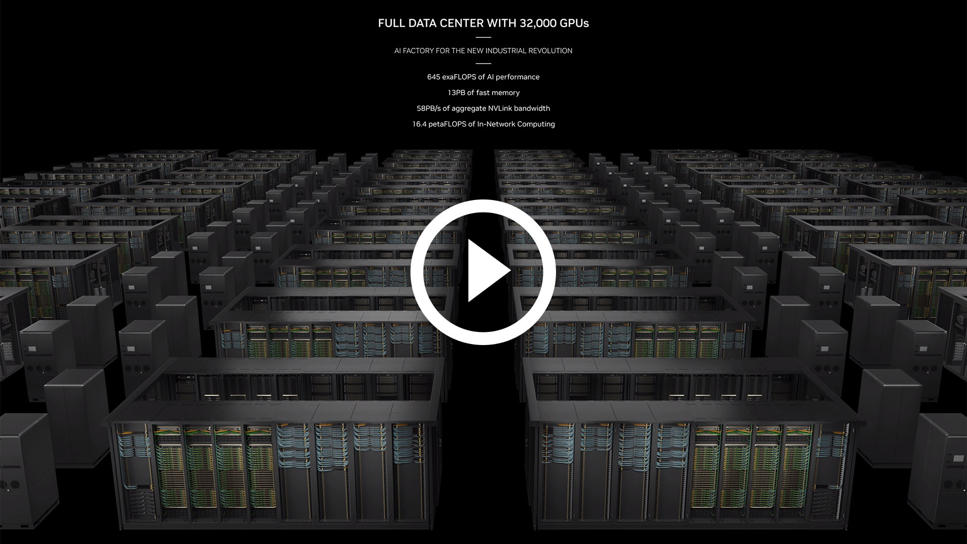
- Rear: Cable Cartridge, ~5,000 copper cables, total length 3.2 km, total weight 1.4 tons
- Top: 2×SN2201 switches + 6-8×33kW power shelves (50V DC bus)
- Bottom: 44U liquid cooling manifold
Topology essence: Complete bipartite graph K_{18,72}. The 18 NVSwitches and 72 GPUs form a complete bipartite graph. Every GPU connects to all 18 NVSwitches, single-hop topology, no intermediate hierarchy.
Bandwidth allocation verification:

"Orthogonal" meaning: Compute nodes insert vertically and switch nodes insert horizontally, perpendicular to each other at the backplane plane. Both types of nodes can be independently removed and inserted. The benefit: compute nodes can be hot-swapped (pulled and replaced on failure), and switch nodes can be independently maintained. But this "independent swapping" is relative — the backplane itself is fixed. If internal backplane traces are damaged, the entire rack must be returned to the factory.
Engineering parameters:
- 78-layer PCB (traditional server motherboards are 12-24 layers, high-end network switch boards are 32-48 layers; 78 layers is unprecedented)
- M9-grade CCL (Dk<3.5, Df<0.002) + Q fabric (quartz fiber cloth) + HVLP4 copper foil — this combination maintains impedance consistency across the 78-layer stack. Dk (dielectric constant) determines signal propagation speed; Df (dissipation factor) determines signal attenuation. M9 grade means Df below 0.002 — the highest grade available in commercial CCL today
- Differential pair count ≥5,184 (18 nodes × 4 ports × 72 pairs/port) [Estimated] — each differential pair must be precisely aligned across 78 layers; impedance deviation in any pair causes increased bit error rate
- Single backplane value >$200,000 (vs Cable Tray ~$30-50K) — a 4-6x cost increase
Why must copper cables be abandoned? The deeper reason: 224G SerDes copper cable transmission distance limit is ~1-2 meters. NVL576 is much larger than NVL72 (144 packages vs 36 packages), and copper cable lengths would inevitably exceed the limit. The orthogonal backplane achieves reliable transmission through precisely impedance-matched PCB traces. Copper cables weren't eliminated because they were "not good enough" — they became unusable at the NVL576 scale.
More specifically: the skin effect of copper cables causes current to concentrate on the conductor surface at high frequencies. At 200G SerDes, the effective transmission distance was already very short; at 224G SerDes, it worsens further. PCB traces can compensate for the skin effect by precisely controlling trace width, spacing, and dielectric layer thickness — something copper cables cannot do, as the geometric consistency of discrete cables cannot be controlled with the same precision as PCB manufacturing.
The costs:
- Yield: 78-layer M9 PCB layer-to-layer alignment accuracy at the micron level, estimated yield 60-70% [Third-party]. This means roughly 1 in 3 boards may be scrapped due to inter-layer alignment deviation. At $200K/board × 30-40% scrap rate = effective cost $280-330K/board
- Maintainability regression: Backplane has fixed connections; if damaged → entire rack returns to factory (vs copper cables which can be unplugged and replaced). A 144-package rack return-to-factory transport + repair cycle is estimated at 2-4 weeks, during which all 576 Dies are completely unavailable
- Capacity bottleneck: M9 CCL is only available from a few suppliers (Shengyi Technology, Tai Guang Electronics), Q fabric from Feilihua with 70% market share. Supply-demand imbalance expected to persist through 2027 [Third-party]. This means Rubin Ultra NVL576 delivery cadence may not be determined by chip capacity but by PCB capacity — a first in NVIDIA's history where a "non-chip factor determines delivery"
- Thermal expansion mismatch: CTE (coefficient of thermal expansion) of the 78-layer PCB doesn't perfectly match the connectors' CTE. Under 400+kW heat load, the internal rack temperature gradient can reach 20-30°C, and different layers of the 78-layer PCB expand at different rates. Over extended operation, this may cause inter-layer microcracks. This problem is difficult to reproduce in lab environments but may surface after 3-5 years of 24/7 data center operation
2.5 Orthogonal Backplane vs Copper Cables: A TCO Analysis
We've analyzed the technical pros and cons above, but the customer's ultimate question is: after switching to the backplane, does the cost per token go up or down?
Using DeepSeek-R1 inference as an example, let's do an order-of-magnitude estimate:
| Cost Item | Dual NVL72 (Copper) | Single NVL576 (Backplane) |
|---|---|---|
| Hardware Cost | 2×NVL72 ≈ $6-7M | 1×NVL576 ≈ $12-15M |
| Interconnect Cost | Cable Tray ×2 ≈ $80-100K + CX-9 IB switch ≈ $300K | Orthogonal backplane ≈ $300K |
| Total Compute (FP4) | 2×1.08 EF = 2.16 EF | 15 EF (7x) |
| Interconnect Bandwidth | 130+130=260 TB/s (NVLink) + IB | 1.5 PB/s (all NVLink) |
| NVLink Domain | 72+72=144 GPU (cross-IB) | 576 Die (single domain) |
| EP Efficiency | EP72×2 cross-IB, all-to-all ~10μs | EP576 single domain, all-to-all ~1μs |
| Power | ~280-300kW | ~400+kW |
| Maintenance | Copper cables swappable, MTTR ~hours | Backplane damage → factory return, MTTR ~weeks |
Per-token cost estimation:
- Dual NVL72 theoretical throughput: 2×226 tok/s/GPU × 72 = 32,544 tok/s (but cross-IB EP efficiency takes a discount, actual ~25,000 tok/s)
- Single NVL576 theoretical throughput: compute is 7x dual NVL72, but EP576's EP communication efficiency is worse than EP72×2 (cross-zone latency). Estimated actual throughput ~120,000-150,000 tok/s
- Per-token cost = (hardware depreciation + electricity + operations) / throughput
- Dual NVL72: ~$3M/year depreciation + $0.3M/year electricity ≈ $3.3M/year → $3.3M / (25000×3600×8760) ≈ $4.2/million tokens
- Single NVL576: ~$6M/year depreciation + $0.5M/year electricity ≈ $6.5M/year → $6.5M / (135000×3600×8760) ≈ $1.5/million tokens
Conclusion: NVL576's per-token cost is approximately 35% of dual NVL72. Although the backplane solution doubles hardware cost, compute increases by 7x, resulting in a dramatically lower per-token cost when amortized.
But there's an important caveat: the above calculation assumes NVL576 has the same availability (uptime) as dual NVL72. In practice, because backplane factory-return MTTR is much higher than copper cable replacement, NVL576's actual availability may be 5-10% lower. Adjusting for 90% availability, per-token cost rises to ~$1.7/million tokens, still 40% of dual NVL72.
Practical implication for customers: If you can only afford 1-2 NVL72s, the copper cable solution remains a reasonable choice. But if you're planning a 100+ rack AI factory, NVL576's per-token cost advantage is hard to ignore — provided you can accept longer repair cycles and higher upfront investment.
3.1 NVLink 5 (Blackwell Architecture)
Core parameters:
- SerDes: 100G→200G
- Per GPU: 18 links × 100GB/s bidirectional = 1.8TB/s
- NVSwitch: 72 ports × 2 × 200Gbps = 14.4TB/s bidirectional
- SHARP engine: In-network reduction within switches, all-reduce communication volume reduced by N times
- Scale-Out: CX-7 400Gb/s + Quantum-2 IB / Spectrum-X Ethernet
SHARP's specific role deserves elaboration. In traditional all-reduce, each GPU sends complete data to all other GPUs (or uses Ring/Tree algorithms), and communication volume grows linearly with GPU count. SHARP performs reduction operations directly inside the NVSwitch — data is reduced as it arrives at the switch, no need to send it back to GPUs for reduction.
Practical effect: For 72-GPU all-reduce, without SHARP each GPU must send 71 gradient copies; with SHARP, each GPU sends only 1 copy to the switch, which reduces and broadcasts the result. Communication volume reduced by approximately N/2 times (N = participating GPU count).
This is especially critical for MoE models: DeepSeek-R1's Expert Parallelism requires all-to-all communication to route tokens to the correct experts. SHARP directly accelerates this step.
3.2 NVLink 6 (Rubin Architecture)
The change is not just bandwidth doubling:
- SerDes: 200G→224G (+12%, doubling comes from doubled channel count)
- Per GPU: 3.6TB/s
- Control plane resilience: Control channels independent of data channels; transient errors don't affect connection state
- Partial deployment operation: Partial tray failures → degraded operation rather than total system failure
- Switch tray hot-swap: NVSwitch online replacement
Why does operational resilience matter? NVL72 single point of failure affecting 72 GPUs is already significant. NVL576 without this capability → any component failure = 576 Dies unavailable. These features are paving the way for NVL576 at scale.
What "partial deployment operation" specifically means: If one of 18 compute trays fails, the system doesn't need to go offline entirely. NVLink 6 switches can reconfigure the topology, isolating the failed node and allowing remaining nodes to continue in degraded mode. This is similar to how a RAID array continues running in degraded mode when one drive fails. In a 576-Die system, this capability is not "nice to have" but "must have" — the failure rate of 576 Dies is far higher than 72.
Bandwidth verification: 72 × 3.6TB/s ÷ 2 × 2 = 259.2TB/s ≈ 260TB/s [Matches official]
3.3 Topology Scaling
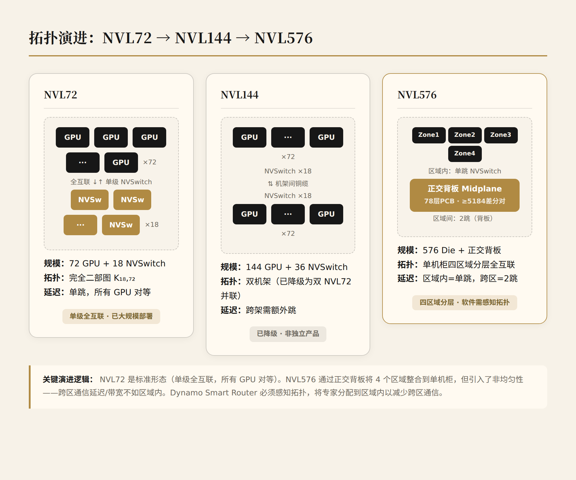
NVL576 hierarchical full interconnect architectural compromises:
- Intra-zone: All-to-all single-hop NVSwitch, latency = NVL72
- Inter-zone: Must traverse the backplane, possibly 2 hops (source zone NVSwitch → backplane → destination zone NVSwitch)
- Inter-zone bandwidth: Limited by backplane differential pair count
In NVL72, all GPUs are peers. In NVL576, cross-zone communication latency/bandwidth is worse than intra-zone. MoE's Expert Parallelism must account for this non-uniformity — software scheduling must be topology-aware. This is one of the Dynamo Smart Router's responsibilities: placing experts within zones to minimize cross-zone communication.
4. Chip Iteration: GPU, CPU, and LPU Advancing on Three Fronts
4.1 GPU: Die Count Exponential Growth and the Per-Die Compute Paradox
| Architecture | Die/Package | Total Dies | Per-Package FP4 | Per-Die FP4 | HBM |
|---|---|---|---|---|---|
| Blackwell | 2 | 72 | ~20P | ~10P | 192GB HBM3e |
| Blackwell Ultra | 2 | 72 | ~30P | ~15P | 288GB HBM3e |
| Rubin | 2 | 72 | ~100P | ~50P | 288GB HBM4 |
| Rubin Ultra | 2+2 modular | 576 | ~104P | ~26P | 1TB HBM4e |
Rubin Ultra's per-Die compute (~26 PFLOPS) is actually lower than Rubin's (~50 PFLOPS/Die). Reason: The 4-Die (actually 2+2) package shares HBM4e interfaces and NVLink bandwidth; per-Die compute density is diluted. Total system compute improvement comes more from scale expansion.
Looking deeper: Blackwell→Rubin per-Die compute went from ~10→~50 PFLOPS (5x), mainly from TSMC 4NP→N3P process upgrade + architecture optimization + HBM4 bandwidth improvement. But Rubin→Rubin Ultra's 4-Die packaging did not bring an equivalent per-Die improvement — it's a "width over depth" strategy.
The qualitative shift of HBM4: Blackwell architecture HBM3e bandwidth is 8TB/s; Rubin architecture HBM4 reaches 22TB/s (2.75x). This bandwidth jump is the key driver of Rubin's per-Die performance leap — many LLM operators in the Decode phase are Memory Bandwidth Bound, and HBM bandwidth directly determines actual throughput.
A concrete number to illustrate: DeepSeek-R1 Decode phase, generating each token requires loading all active experts' weights. Assuming per-expert parameters of 44M (DeepSeek-V3 data), at FP8 precision that's 44MB. Loading from HBM3e (8TB/s) takes 5.5μs; from HBM4 (22TB/s) takes 2μs. For 256-expert EP communication, this gap gets amplified 256 times.
4.2 CPU: From Grace to Vera — A Role Transformation for the Agentic AI Era
| Dimension | Grace | Vera Olympus |
|---|---|---|
| Architecture | Arm v9 | Arm v9.2 |
| Core Count | 72 | 88 (+22%) |
| Thread Count | 144 | 176 |
| Process | TSMC 5nm | TSMC 3nm |
| Memory/Chip | ~1TB LPDDR5X | 1.5TB LPDDR5X [Official] |
| Memory Bandwidth | ~500GB/s | 1.2TB/s [Official] |
| NVLink-C2C | 900GB/s | 1.8TB/s [Official] |
| Transistor Count | ~Not disclosed | 227 billion [Official] |
The CPU's role in the supernode is undergoing a qualitative transformation. The traditional view is that the CPU is a "subordinate managing GPUs," but Agentic AI changes this equation:
- Multi-Agent scheduling: Agent loops frequently trigger context switches, process scheduling, sandbox creation/destruction — all CPU work. An Intel paper shows that in most Agent workloads, CPU time can account for 40%-90% of end-to-end latency [Third-party]. This means that even in GPU-intensive inference scenarios, CPU performance directly limits system throughput.
- KV Cache offloading: Long-context KV Cache consumes GPU memory; the industry commonly offloads idle KV Cache to CPU memory + SSD. Grace CPU's ~500GB/s memory bandwidth may become a bottleneck when handling large-scale KV Cache transfers. This is the direct reason Vera increased bandwidth to 1.2TB/s. Specifically: 128K context, FP8 KV Cache, ~2MB KV Cache per token; 100 concurrent requests = 200GB of KV Cache data. Moving from GPU memory to CPU memory at 500GB/s takes 0.4s; at 1.2TB/s, it drops to 0.17s.
- Tool call orchestration: High-concurrency Agents extensively invoke retrieval, coding, browsing, and other tools; non-inference tasks are handled by the CPU. NVIDIA Dynamo's Smart Router runs on the CPU, needing to traverse the Radix Tree for KV Cache matching — CPU core count and memory bandwidth directly determine routing latency.
Guojin Securities' May 2026 report notes: AMD projects global server CPU TAM to reach $120 billion by 2030; Arm projects data center CPU market to exceed $100 billion. The CPU/GPU ratio is evolving from HGX-era 1:4 and 1:8 toward 1:2, 1:1, or even higher. Vera's doubled core count and NVLink-C2C bandwidth are not coincidences.
4.3 LPU: The "Seventh Member" — But Jensen Huang Says It's a "Niche Product"
⚠️ Updated 2026-05-21 (Q1 FY2027 Earnings Call): Jensen Huang explicitly positioned the Groq 3 LPU as a "niche product for some time." His exact words: "LPX is designed for low latency and high token rate, but its throughput is low. The use case for LPX is not broad." This means LPU's strategic weight within NVIDIA's product matrix has been downgraded from the high-profile "seventh chip" positioning at GTC 2026 to a scenario-specific supplement. The analysis below was written post-GTC and is retained for technical reference, but should be read in light of Jensen's updated positioning.
Groq 3 LPX is an independent supernode form factor that doesn't participate in the NVLink domain, coordinating with Vera Rubin NVL72 via Ethernet:
| Dimension | Vera Rubin NVL72 | Groq 3 LPX |
|---|---|---|
| Positioning | Training + Prefill + Attention | Decode FFN + Speculative Decoding |
| Chip | GPU (HBM4) | LPU (pure SRAM) |
| Count | 72 GPU + 36 CPU | 256 LPU |
| Memory | 20.7TB HBM4 | 128GB SRAM + 8TB DDR |
| SRAM Bandwidth | N/A | 40 PB/s |
| Power | ~200kW | ~80-100kW [Estimated] |
| Interconnect | NVLink 6 | C2C 112G SerDes, Dragonfly |
| Software | CUDA + Dynamo | Groq compiler + Dynamo |
LPX's essence: Not an NVL replacement, but an inference-dedicated acceleration layer. GPU's HBM capacity and compute density suit Prefill/Attention; LPU's SRAM bandwidth (150TB/s/chip, ~7x HBM4) suits FFN Decode. Through Dynamo orchestration, AFD (Attention-FFN Disaggregation) splits inference across both hardware types.
AFD only matters for Agentic inference — training is still purely GPU. This is why Rubin CPX was killed: it solved Prefill cost, but the market's biggest pain point is Decode speed. LPU uses SRAM to directly attack Decode's "memory wall."
LPX's internal interconnect uses Dragonfly topology (256 LPUs fully interconnected via C2C 112G SerDes), not NVLink. Each LPU has 96 C2C links: 56 for full interconnect within the ComputeTray, 31 for cross-Tray interconnect, 4 connecting to the Fabric Expansion Logic FPGA, and the rest for cross-rack.
Fabric Expansion Logic is LPX's key innovation — it provides an FPGA + 256GB DDR on each ComputeTray for prefetching MoE expert parameters from DDR to SRAM. Bandwidth breakdown: DDR5-6400 quad-channel 204.8GB/s, distributed across 256 LPUs = only 200Gbps/LPU — this bandwidth is far below SRAM bandwidth (150TB/s), meaning expert loading time is approximately 1.68μs (44MB expert / 204.8GB/s), plus ~2μs compute time. Each token's FFN expert layer execution time is approximately 4μs. 256-expert EP communication must be layered on top of this with all-to-all communication — zartbot's real-world simulation has detailed data on this.
4.4 System Design Ratio Evolution: Hardware Coupling Logic Under the Roofline Model
Previous sections listed specifications, but didn't answer a more fundamental question: Why did NVIDIA choose these specific numbers for each generation? Why does NVLink bandwidth go from exactly 1.8→3.6 TB/s, not 2.0 or 4.0? Why did HBM bandwidth jump 2.75x from 8→22 TB/s, far exceeding NVLink's 2x?
The answer lies in a key concept: Arithmetic Intensity.
What is Arithmetic Intensity, and Why Does It Determine GPU Design?
Arithmetic Intensity = Computation (FLOPs) / Memory Access (Bytes), measured in FLOPs/Byte. It measures "how many operations are performed for every byte read from memory."
Every GPU has a hardware ridge point:

No parameter is optimized independently. HBM bandwidth determines the ceiling for Decode performance; NVLink bandwidth determines the viable width of EP; L2 Cache determines the reuse efficiency of high-frequency experts; FP4/NVFP4 is the unified compensation scheme for all bandwidth constraints. NVIDIA finds the optimal balance point in this coupled system every generation.
With this logic in mind, the tables above are no longer a collection of isolated numbers, but a precision-coupled engineering design — every parameter change has a "because... therefore..." causal chain.
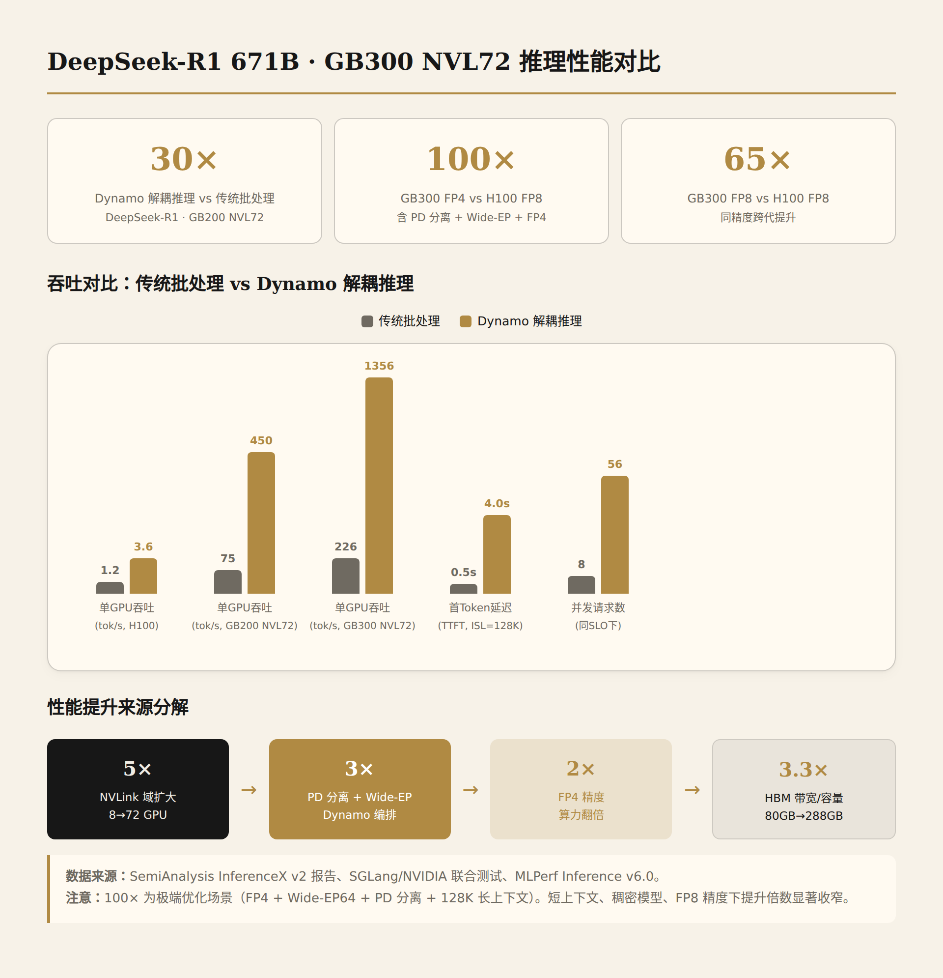
5. Benchmark Data Evolution: From H100 to GB300 NVL72 — Quantifying the Inference Leap
This chapter is the most important new content in this article. Previous analyses covered specs and estimates; now we use real test data to validate theoretical expectations.
5.1 Cross-Generation Inference Performance Comparison (Third-Party Benchmarks)
The following data comes from the SemiAnalysis InferenceMAX report, CoreWeave real-world testing, and MLPerf Inference v5.1/v6.0. The test model is DeepSeek-R1 671B (MoE architecture).
| Metric | H100 HGX 8-card | GB200 NVL72 | GB300 NVL72 | Improvement (vs H100) |
|---|---|---|---|---|
| Per-GPU Throughput (DeepSeek-R1) | ~1.2 tok/s/GPU | ~75 tok/s/GPU | ~226 tok/s/GPU | 188x (GB300) |
| FP4 vs FP8 | FP8 | FP8 | FP4 | FP4 additional 2x |
| Parallelism Strategy | TP16 | EP64 | EP64+PD Disaggregation+Wide-EP | Strategy evolution |
| NVLink Domain | 8 GPU | 72 GPU | 72 GPU | Domain 9x larger |
| HBM Capacity/GPU | 80GB | 192GB | 288GB | 3.6x |
Data Sources and Interpretation:
-
H100 baseline: ~1.2 tok/s/GPU; TP16 means 16-card tensor parallelism requiring 4×8-card nodes connected via IB. All-to-all communication traverses the IB network; latency is the primary bottleneck. MoE Expert Parallelism can't be effectively deployed within an 8-card domain — 256 experts distributed across 16 GPUs means 16 experts per GPU, and Expert All-to-All communication volume is enormous.
-
GB200 NVL72: ~75 tok/s/GPU [SemiAnalysis/Signal65], measured at FP8 precision with EP64 parallelism. 75 tok/s/GPU × 72 GPU = 5,400 tok/s total rack throughput. Performance improvement comes from three factors:
- NVLink domain from 8→72: EP communication no longer traverses IB network; all-to-all latency drops from millisecond-level to microsecond-level
- HBM 80→192GB: Can accommodate larger KV Cache, reducing offload
- 30TB shared memory: CPU+GPU unified addressing, shorter KV Cache offload path
-
GB300 NVL72: ~226 tok/s/GPU [SGLang/NVIDIA joint testing], FP4 precision, ISL=128K/OSL=8K. 226 tok/s/GPU × 72 = 16,272 tok/s total rack throughput. 3x improvement over GB200, from:
- FP4 vs FP8: Compute doubles (Blackwell Ultra natively supports FP4 Tensor Cores)
- 288GB HBM3e: More memory for longer contexts + more concurrency; 128K context is no longer a bottleneck
- FMHA kernel optimization: Attention computation efficiency improved 1.35x [SGLang]
- PD Disaggregation + Wide-EP: Decoupled inference orchestrated by Dynamo (see Section 5.2)
-
MLPerf Inference v6.0 record: GB300 NVL72 achieved 8,064 tokens/sec/GPU on DeepSeek-R1 server-side testing [MLPerf v6.0]. Note the difference from 226 — MLPerf uses offline/server-side scenarios with potentially different batch strategies and ISL/OSL configurations. The single-version improvement from MLPerf v5.1→v6.0 was 2.77x, indicating that software optimization (TensorRT-LLM kernel fusion + Dynamo PD disaggregation) contributed enormously.
5.2 Software Stack Generational Evolution
Hardware spec improvements are only half the story. From H100 to GB300, software stack evolution is equally critical — in some scenarios, software optimization contributed more than hardware upgrades.
| Software Capability | H100 Era (2023) | GB200 Era (2024) | GB300 Era (2025-26) | Vera Rubin (2026H2) |
|---|---|---|---|---|
| Inference Engine | TensorRT-LLM initial | TensorRT-LLM mature | TRT-LLM + vLLM + SGLang | Same |
| Disaggregated Inference | None | None | Dynamo PD Disaggregation | Dynamo 1.0 AFD |
| KV Cache Management | GPU memory only | Memory + CPU offload | Distributed KV Cache Pool | Multi-tier storage offload |
| Parallelism Strategy | TP8 | TP+PP+DP | +Wide-EP+Chunked-PP | +AFD (GPU+LPU) |
| Precision | FP16/BF16 | FP8 | FP8+FP4 | NVFP4 |
| Routing | Round-robin | Load-balanced | LLM-aware intelligent routing | Topology-aware routing |
| GPU Scheduling | Static allocation | Static allocation | Dynamic Planner | Dynamic + cross-hardware |
Key insight: From GB200 to GB300, the hardware spec increment is modest (FP4 support + HBM capacity + CX-8), but inference performance improved 3x. This 3x comes primarily from software: Dynamo's PD disaggregation, Wide-EP, Chunked-PP, and FMHA kernel optimization. This is a classic case of "hardware defines the ceiling; software determines actual performance."
5.3 SemiAnalysis Benchmark: The Full Curve from 30x to 100x
SemiAnalysis InferenceX v2 report provides the most complete cross-generation comparison. Core conclusion:
Jensen Huang's "30x inference improvement" claim at GTC 2024 was indeed conservative. Benchmark data:
| Comparison Scenario | Baseline | GB300 NVL72 Performance | Multiplier |
|---|---|---|---|
| FP4 vs FP8 (H100) | H100 FP8 | GB300 FP4 | ~100x |
| FP8 vs FP8 | H100 FP8 | GB300 FP8 | ~65x |
| FP8 vs FP8 (same Dynamo) | H100+Dynamo | GB300+Dynamo | ~30x |
| MoE scenario vs AMD | MI355X | GB300 | ~28x |
But note the scenario dependency. 100x is an "extreme optimization scenario" — FP4 precision, Wide-EP64, PD disaggregation, 128K long context. With short contexts (<4K), dense models, and FP8 precision, the improvement multiple narrows significantly.
Power efficiency evolution is more convincing:
| Metric | H100 | GB300 NVL72 | Multiplier |
|---|---|---|---|
| Throughput per Watt | Baseline | 5x | [NVIDIA Official] |
| Cost per token | Baseline | 1/35 | [NVIDIA Official] |
| vs AMD MI355X per-token cost | N/A | 1/15 | [Signal65] |
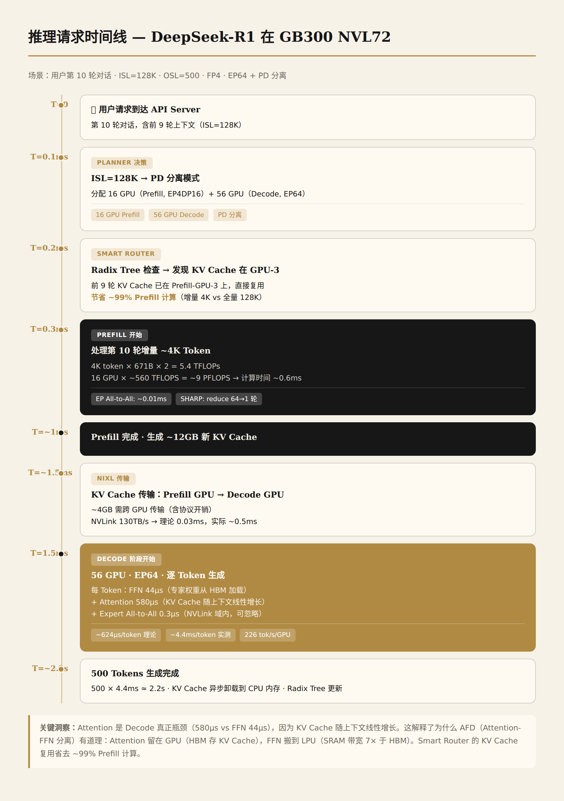
5.4 A Token's Complete Journey: DeepSeek-R1 on GB300 NVL72
We've listed numbers above, but readers may still lack an intuitive "feel." Let's trace the full lifecycle of an Agentic inference request and see where the time is spent at each step.
Scenario: User sends the 10th round of conversation, ISL=128K (including previous 9 rounds of context), expecting OSL=500 tokens. Model: DeepSeek-R1 671B MoE, 256 routing experts, top-8 routing.
Key insights from the timeline:
-
Attention is the real bottleneck in Decode (580μs vs FFN 44μs). This is because KV Cache grows linearly with context length, while FFN expert weight sizes are fixed. This explains why AFD (Attention-FFN Disaggregation) makes sense: keep Attention on GPU (which has HBM to store KV Cache), and move FFN to LPU (SRAM bandwidth 7x HBM; pure weight loading is extremely fast).
-
NVLink bandwidth is more than sufficient for EP scenarios (Expert All-to-All 0.3μs vs HBM load 44μs). This isn't coincidence — NVIDIA deliberately designs NVLink bandwidth to "far exceed EP communication needs," ensuring EP isn't bottlenecked by interconnect. The real bottleneck is always HBM.
-
Smart Router's KV Cache reuse saves ~99% of Prefill computation (incremental 4K vs full 128K). In Agentic scenarios, Smart Router reuse across 10 rounds of conversation can reduce total Prefill time from seconds to milliseconds.
-
The theoretical lower bound for a single Decode token is approximately 624μs, but measured is 4.4ms/GPU (including batch scheduling). The gap comes from batch coalescing, GPU scheduling overhead, and Continuous Batching queue wait times. This means there's still ~7x optimization headroom in software scheduling.
6. Software Stack Deep Dive: Why Dynamo Is the "OS of the AI Factory"
6.1 From Triton to Dynamo: A Paradigm Shift in Inference Frameworks
When NVIDIA released the Triton Inference Server in 2018, AI inference was still a "single GPU running a single model" world. Tritin solved the framework unification problem (TensorFlow/PyTorch/ONNX unified deployment), but facing 2025-2026 inference scenarios — 671B-parameter MoE models distributed across 72 GPUs — it was out of its depth.
The fundamental difference: Triton manages "model deployment"; Dynamo manages "distributed inference orchestration." Specifically:
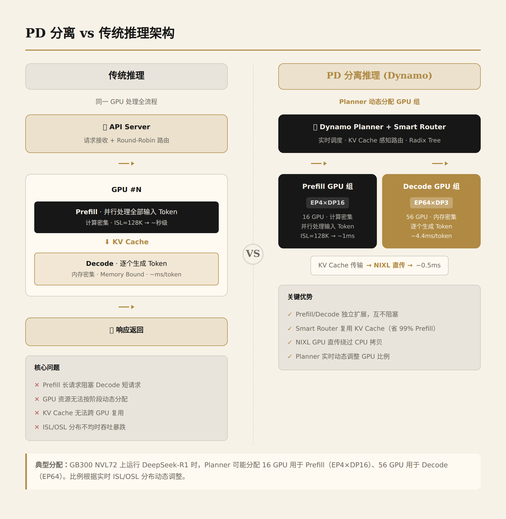
- Triton: one request → one GPU processes → returns result. No matter how large the model, just slice it more
- Dynamo: one request → split into Prefill + Decode phases → assigned to different GPU groups → KV Cache migrates between GPUs → dynamically adjusts GPU allocation → merges results. Each phase can use different parallelism strategies
This ability to "split requests" is Dynamo's core innovation, and why NVIDIA calls it the "OS of the AI factory" — it doesn't just deploy models, it orchestrates the entire inference pipeline.
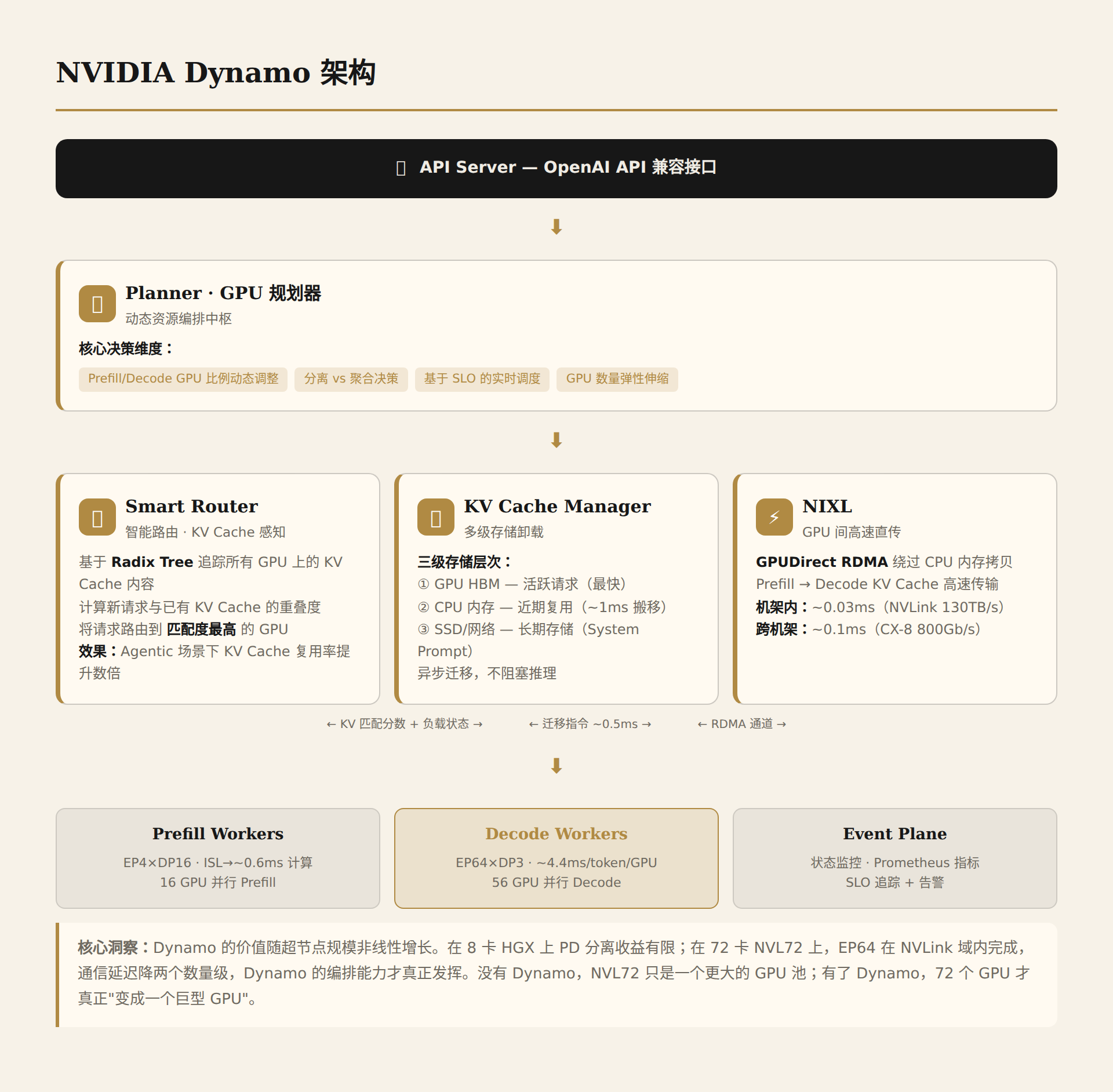
6.2 Dynamo Architecture: Four Core Components
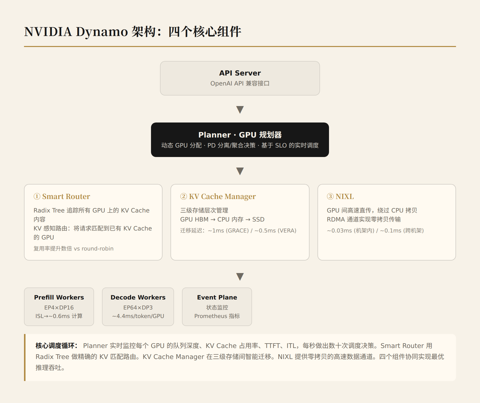
1. Planner (GPU Planner)
This is not simple load balancing. The core problem the Planner faces: each request's Prefill and Decode phases have extremely uneven workloads.
For example: a summarization request with 128K context (ISL=128K, OSL=500). Prefill needs to process 128K tokens of compute-intensive forward pass; Decode only needs to generate 500 tokens one by one. If Prefill GPUs and Decode GPUs are split 50/50, long-input requests will cause Prefill GPU backlog while Decode GPUs idle.
Planner's decision dimensions:
- Prefill/Decode GPU ratio: Dynamically adjusted based on real-time ISL/OSL distribution
- Disaggregation vs aggregation: Short-input requests (ISL<2K) may not need PD disaggregation; processing directly on one GPU is more efficient
- GPU count elasticity: During peak demand, temporarily allocate more GPUs to Prefill; during low demand, reclaim them
These decisions are real-time — the Planner continuously monitors each GPU's queue depth, KV Cache utilization, TTFT (time to first token), and ITL (inter-token latency), potentially making dozens of scheduling decisions per second.
2. Smart Router (Intelligent Router)
Traditional load balancers use round-robin or least-connections routing. Dynamo's Smart Router is different: it uses a Radix Tree to track KV Cache content across all GPUs, calculates the overlap between new requests and existing KV Cache, and routes requests to the GPU with the highest KV Cache match.
Why does this matter? Consider an Agentic scenario: a user has had 10 rounds of conversation with an Agent; the first 9 rounds' KV Cache is already on GPU-7. When the 10th round request arrives, the Smart Router routes it directly to GPU-7, reusing existing KV Cache and avoiding recomputing the first 9 rounds of context.
NVIDIA's data: In a 2-node HGX-H100 (16 GPU) test with DeepSeek-R1-Distill-Llama-70B on 100K real R1 requests (average ISL/OSL=4K/800), the Smart Router significantly reduced response time compared to round-robin, with KV Cache reuse rate increased several fold. [NVIDIA Developer Blog]
3. KV Cache Manager
KV Cache is the largest memory consumer in LLM inference. 128K context, FP8 precision, 671B MoE model — a single request's KV Cache can reach hundreds of MB to several GB. With hundreds of concurrent requests across 72 GPUs, total KV Cache can reach tens to hundreds of GB.
KV Cache Manager implements a three-tier storage hierarchy:
- GPU HBM (fastest, most expensive): KV Cache for active requests
- CPU memory (medium): Recently completed but potentially reusable KV Cache
- SSD/network storage (slowest, cheapest): Long-term storage of potentially reusable KV Cache (e.g., system prompts)
Key innovation: KV Cache migration between the three tiers is asynchronous, not blocking inference. After the GPU finishes generating tokens, KV Cache is moved to CPU memory in the background; when a new request arrives, if KV Cache is in CPU memory, it's transferred back to GPU HBM at high speed via NVLink-C2C.
Grace CPU's NVLink-C2C bandwidth is 900GB/s (Vera increases to 1.8TB/s), meaning 1GB of KV Cache moves from CPU memory to GPU HBM in ~1ms (Grace) or ~0.5ms (Vera). This is virtually imperceptible to performance.
4. NIXL (NVIDIA Inference Transfer Library)
NIXL is the most understated yet most critical component in Dynamo — it solves the problem of "high-speed KV Cache transfer between GPUs."
In PD disaggregation architecture, after Prefill completes, KV Cache must be transferred from Prefill GPU to Decode GPU. If both GPUs are within the same NVL72 rack, NVLink transfer at 130TB/s is fast. But in cross-rack (Scale-Out) scenarios, the traditional path is GPU→CPU memory→NIC→network→NIC→CPU memory→GPU, involving multiple copies.
NIXL enables GPU→GPU direct transfer via GPUDirect RDMA, bypassing CPU memory copies. Combined with CX-8's 800Gb/s bandwidth, cross-rack KV Cache transfer latency drops from millisecond-level to hundred-microsecond-level. [NVIDIA Developer Blog]
6.3 Dynamo Performance Across Different Supernodes
| Software Optimization | Without NVL72 (8-card) | GB200 NVL72 | GB300 NVL72 | Vera Rubin NVL72 |
|---|---|---|---|---|
| PD Disaggregation Effect | Limited (small EP domain) | Significant (72-card EP domain) | 3x over GB200 | Higher (260TB/s) |
| Wide-EP | Not feasible (EP>8 requires cross-node) | EP64 feasible | EP64+FP4 | EP72+NVFP4 |
| KV Cache Offload | Limited CPU memory | 30TB shared | 40TB shared | More + SSD tier |
| Smart Router | 8 cards don't need complex routing | 72 cards need it | 72 cards need it | 576 Dies must have it |
| Dynamo Measured Improvement | ~2x (Llama 70B) | ~30x (DeepSeek-R1) | Same + FP4 extra 2x | Pending validation |
Core insight: Dynamo's value grows non-linearly with supernode scale. On 8-card HGX, PD disaggregation benefit is limited — because the EP domain is too small, MoE Expert All-to-All communication still traverses the IB network. On 72-card NVL72, EP64 completes within the NVLink domain, and communication latency drops by two orders of magnitude. Only then does Dynamo's orchestration capability truly shine.
This means: NVL72's hardware advantage is not independent, but coupled with Dynamo. Without Dynamo, NVL72 is just a larger GPU pool; with Dynamo, 72 GPUs truly "become one giant GPU."
6.4 SHARP: The Hidden In-Network Compute Accelerator
SHARP (Scalable Hierarchical Aggregation and Reduction Protocol) is a hardware acceleration engine within NVSwitch that directly executes collective communication operations like all-reduce/broadcast inside the switch.
Why is this important? Take DeepSeek-R1's Expert Parallelism as an example:
256 experts distributed across 64 GPUs (Wide-EP64). Every token routing requires all-to-all communication. Traditional approach: each GPU sends 64 gradient copies to all other GPUs, totaling 64×64=4,096 transfers. SHARP approach: each GPU sends 1 copy to NVSwitch, which performs the reduction internally and broadcasts the result — communication reduced by approximately 32x.
SHARP existed in the NVLink 5 era, but NVLink 6 switches have enhanced SHARP engine throughput and supported collective communication types. In MoE inference scenarios, SHARP can accelerate Expert All-to-All by 2-4x (depending on GPU count and expert allocation strategy). [NVIDIA]
7. Power and Thermal: From Cold Plates to Microchannels
| Architecture | Per-GPU Power | Rack Power | Cooling Solution | Power per EFLOPS |
|---|---|---|---|---|
| Blackwell | ~1000W | ~120kW | Cold plate liquid cooling | 167 kW/EFLOPS |
| Blackwell Ultra | ~1400W | ~140-150kW | Cold plate liquid cooling + enhanced | 130 kW/EFLOPS |
| Rubin | ~2000W | ~200kW | Full liquid + microchannel cold plate | 56 kW/EFLOPS |
| Rubin Ultra | ~2000W+ | ~400+kW | Full liquid + microchannel + phase change (possible) | 27 kW/EFLOPS |
2000W/GPU is the physical limit of cold plate liquid cooling. Reason:
Chip area is fixed (~800mm²). Heat flux density = 2000W / 800mm² ≈ 2.5 W/mm². Traditional cold plate microchannels can only cover part of the chip surface; cooling efficiency drops at the edges.
Beyond this threshold requires:
- Microchannel lids: Microfluidic channels (50-200μm) machined into the GPU lid, coolant "hugs" the chip to remove heat. Manufacturing process similar to semiconductor lithography; high cost but excellent results — temperature gradient drops from 10-15°C (traditional cold plate) to under 5°C
- Cold plate + immersion hybrid: Cold plate removes ~60%, fluorinated liquid immersion removes ~40%. Immersion cooling's boiling-point cooling (two-phase immersion) forms bubbles at the chip surface to carry away heat; extremely high cooling efficiency but fluorinated liquid is expensive (3M Novec series ~$500/L)
- Phase-change cooling: Low boiling point medium (electronic fluorinated liquid) evaporates at the chip surface absorbing heat. Vapor rises → condenses → flows back, forming a self-sustaining cycle. No pump required, but system design complexity increases dramatically
Rubin Ultra's thermal solution is not fully disclosed yet; multiple supply chain sources point to a microchannel + phase change hybrid solution. [Third-party, unverified]
A number worth calculating: Vera Rubin NVL72 rack ~200kW, assuming PUE=1.1, the data center needs to provide ~220kW of power and cooling capacity. Rubin Ultra NVL576 rack ~400+kW; if PUE is unchanged, a single cabinet needs ~440kW — this is already the total power of a mid-size enterprise data center. Supernode power growth is approaching infrastructure limits.
Microsoft Azure has deployed the world's first GB300 NVL72 production cluster — 64 liquid-cooled racks, 4,608 Blackwell Ultra GPUs. [Third-party] To deploy an equivalent number of Rubin racks, power would increase from ~9MW to ~13MW, placing enormous pressure on existing data center power and cooling systems.
The good news from an energy efficiency perspective: Power per EFLOPS dropped from Blackwell's 167kW to Rubin Ultra's 27kW (6x improvement). But the absolute power growth rate (120→400kW) exceeds most data centers' capacity. AI data center construction speed is being held back by power infrastructure.
8. Where Did NVL144 Go? A Skipped Supernode
This is the most easily overlooked turning point in supernode evolution.
At GTC DC in October 2025, NVIDIA announced Vera Rubin NVL144 — 144 GPUs in a dual-rack NVLink domain. Official specs: 3.5 EFLOPS FP4 inference, 75TB high-speed storage, NVLink + CX9 communication bandwidth of 260TB/s and 28.8Tb/s respectively.
But at the GTC 2026 (March 2026) roadmap, NVL144 was downgraded to a "dual NVL72 in parallel" solution, rather than an independent single-rack product.
My judgment: two reasons.
Physical constraint: 224G SerDes copper cable transmission distance limit is approximately 2 meters (vs 200G's 2-3 meters). NVL144 requires a dual-rack NVLink domain, meaning copper cables must span the distance between two racks (at least 0.5-1 meter of routing + connectors). At 224G speeds, signal integrity over this distance cannot be guaranteed. Even using PCB-embedded copper traces (the Vera Rubin NVL72 approach), cross-rack connections still require some form of external cable or connector.
Product logic: Customers can directly buy two NVL72s and connect them via CX-9 InfiniBand (1.6Tb/s), achieving nearly equivalent Scale-Out performance. An independent NVL144 would require additional NVLink cross-rack switching hardware (high cost, reliability risk), but with limited performance gain — not worth developing as a standalone product.
Deeper product cadence implication: NVIDIA chose to "skip the intermediate state and wait for the endgame solution." True Scale-Up expansion is deferred to Rubin Ultra NVL576 — achieving 576-Die interconnect within a single cabinet via orthogonal backplane, completely bypassing cross-rack copper cables. This means:
- NVL72 is the only mature Scale-Up unit, maintaining 72-GPU scale across both Blackwell and Rubin generations
- NVL576 is NVIDIA's ultimate answer for Scale-Up expansion, but won't arrive until 2027H2
- Intermediate Scale-Out (CX-9 InfiniBand/Spectrum-X) carries most multi-rack expansion duties in 2026-2027
Impact on customers: in 2026-2027, your choices are "single NVL72" or "multi-NVL72 + InfiniBand." There is no "single NVL144" option.
9. Vera Rubin POD: Five Rack Types Making One Supercomputer
The Vera Rubin POD disclosed at GTC 2026 is the ultimate form of the supernode concept — 5 specialized rack types composing an AI supercomputer:
| Rack Type | Role | Core Components | Key Capability |
|---|---|---|---|
| NVL72 Rack | Compute Engine | 72 Rubin GPU + 36 Vera CPU | Training + Prefill + Attention |
| LPX Rack | Inference Acceleration | 256 Groq 3 LPU | Decode FFN + Speculative Decoding |
| STS Storage Rack | KV Cache Extension | BlueField-4 DPU + SSD | Inference context memory storage |
| XTS Rack (Ethernet) | Scale-Out Extension | Spectrum-X Ethernet switch | Cross-POD Ethernet interconnect |
| XTS Rack (IB) | IB Extension | Quantum-X800 IB switch | Cross-POD InfiniBand interconnect |
Complete POD specs: 40 racks, ~20,000 Dies, 60 EFLOPS, 10 PB/s expansion bandwidth, ~1.2 trillion transistors. [Official]
This isn't a "supernode" — it's an AI supercomputer. NVIDIA's product evolution from "selling GPU chips" to "selling AI supercomputers" is most clearly embodied in the POD architecture.
The Dynamo software stack is the key thread connecting everything — it's responsible for splitting inference requests into Prefill (→NVL72) and Decode (→LPX), managing KV Cache offloading and sharing (→STS), and coordinating cross-POD load balancing (→XTS). Without Dynamo, these five rack types are just unrelated hardware. With Dynamo, they form an organic whole.
The POD demands on the software stack far exceed current Dynamo capabilities. AFD (Attention-FFN Disaggregation) requires orchestrating the inference pipeline across GPU and LPU — two heterogeneous hardware types. This is still in early stages in 2026. Dynamo 1.0 supports PD disaggregation and Wide-EP, but AFD cross-hardware orchestration is a capability that can only be truly tested when Vera Rubin enters mass production.
9.1 AFD in Action: An Inference Request Across Three Hardware Types
Scenario: The same Agentic request (ISL=128K, OSL=500), but this time running on a complete Vera Rubin POD — NVL72 for Attention, LPX for FFN Decode, and STS for long-term KV Cache storage.
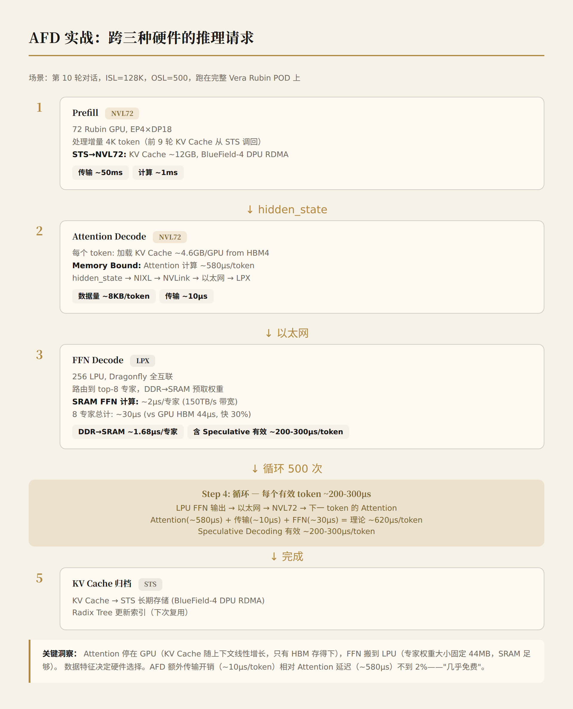
Key insights on AFD:
-
Attention stays on GPU, FFN moves to LPU — the reason isn't "which is faster," but data characteristics. KV Cache grows linearly with context (128K→256GB); only GPU's HBM (288GB/Rubin) can store it. FFN expert weights are fixed size (44MB/expert); LPU's SRAM (0.5GB/LPU) + DDR (256GB/Tray) is sufficient. Data characteristics determine hardware selection, not the other way around.
-
AFD's extra transfer overhead (~10μs/token via Ethernet) is negligible relative to Attention latency (~580μs). This means AFD is "almost free" — overhead is under 2%. But the prerequisite is sufficient network bandwidth and low-latency Ethernet (Spectrum-X).
-
Speculative Decoding is LPU's killer capability. LPU's deterministic execution (no GPU warp divergence or cache thrashing) makes single forward pass time completely predictable, enabling precise prediction of which candidate tokens will be accepted. GPU can't do this — its execution time variance (coefficient of variation CV≈0.3-0.5) makes speculative decoding much less efficient.
Engineering challenges of cross-hardware AFD orchestration: The flow described above requires Dynamo to simultaneously manage two programming models — CUDA (GPU) and Groq compiler (LPU) — dynamically selecting target hardware at runtime and managing cross-hardware data transfers. Dynamo 1.0 supports PD disaggregation and Wide-EP, but AFD cross-hardware orchestration is the capability that can only be truly tested when Vera Rubin enters mass production — this is NVIDIA's biggest software engineering challenge after acquiring Groq.
10. Risks, Challenges, and Counterarguments
10.1 Orthogonal Backplane Is Not a Panacea
Maintainability regression is the biggest problem. In the copper cable architecture, any single link failure can be pinpointed to a specific cable and replaced (time-consuming but feasible). With the orthogonal backplane, a Mezzanine connector solder joint or internal trace failure → entire rack returns to factory. In a 144-package cabinet, this means 144 GPUs simultaneously unavailable until repair is complete.
Whether this is acceptable depends on MTBF. NVIDIA hasn't officially published NVL576 MTBF expectations, but considering the system complexity of 576 Dies + thousands of connectors + 78-layer PCB, industry estimates put first system-level MTBF in the 5,000-10,000 hour range. [Third-party, uncertain] If calculated at 8,000 hours MTBF, a 1,000-rack AI factory would average ~90 rack-return-to-factory failure events per month. Is this magnitude acceptable? That depends on repair time (MTTR) and redundancy design.
Capacity bottleneck: M9 CCL (Shengyi Technology, Tai Guang Electronics) + Q fabric (Feilihua 70% share) + HVLP4 copper foil (Defu Technology, etc.) global capacity is limited. Guojin Securities reports indicate the supply-demand imbalance is expected to persist through 2027. This means Rubin Ultra NVL576 delivery cadence may be determined not by chip capacity but by PCB capacity — a first in NVIDIA's history where a "non-chip factor determines delivery."
10.2 The "8-Year 1000x" Baseline Problem
NVIDIA claims "8-year 1000x compute growth." But decomposing this number:
- Data format changes: FP16→FP8→FP4; each "precision downgrade" nominally doubles compute. But this isn't "same computation faster" — it's "approximating the same result with fewer bits"
- Multi-Die packaging: Blackwell from 1-Die→2-Die (compute doubles but transistors double), Rubin Ultra→4-Die (same logic)
- System scale: NVL72→NVL576, Die count increases 8x
If we look at per-Die, same precision (FP8) actual performance improvement: Hopper→Blackwell approximately 1.5-2x (TSMC 4N→4NP process dividend is limited), Blackwell→Rubin approximately 3-3.5x (TSMC 4NP→N3P + HBM4 + architecture optimization). True per-Die generational improvement is in the 2-3x range, far below the annual growth rate implied by "1000x."
This isn't to say NVIDIA is faking numbers — system-level compute is indeed growing rapidly. But the primary source of growth is shifting from "faster chips" to "bigger systems + lower precision."
Real-world data also confirms this: Of the 100x improvement from H100 to GB300 NVL72, FP4 contributed 2x, NVLink domain expansion contributed ~5x (EP efficiency), Dynamo PD disaggregation contributed ~3x, and HBM capacity/bandwidth contributed ~3x. Hardware and software each account for roughly half the credit.
10.3 Photonics Is the Endgame
Intel's SC25 report clearly states: 2028 is the endgame for copper. NVL576's orthogonal backplane is essentially "using PCB copper traces to replace copper cables" — still copper.
NVIDIA has already introduced 200G silicon photonics CPO (co-packaged optics) in Spectrum-X switches, but hasn't yet extended it to GPU-to-GPU NVLink domains. The Feynman architecture (2028 production) is expected to switch NVLink's LPU C2C bus to CPO architecture. [Third-party, inferred from NVIDIA roadmap]
If this materializes, the orthogonal backplane may exist for only one generation (Rubin Ultra) before being replaced by photonic interconnects. This means the massive investment in 78-layer M9 PCB orthogonal backplanes may have a product lifecycle of only 1-2 years.
But CPO itself carries risks: silicon photonics coupling efficiency, packaging yield, power consumption (laser arrays consume non-trivial power), and cost (current CPO module unit price is far higher than copper interconnects) are all unresolved engineering challenges.
10.4 The Power Wall Remains Unresolved
From NVL72 to NVL576, rack power ~120→400+kW (3.3x). Extrapolating this trend:
- Feynman architecture (~2028): Could reach 1MW/cabinet
- This is already approaching the total power of a mid-sized data center
- North American data center power and site selection bottlenecks are becoming increasingly acute
- Microsoft, Google, Meta have already been investing in nuclear, geothermal, and other non-traditional energy sources
The marginal cost of performance improvement is rising sharply. Power per EFLOPS improved from Blackwell's ~120kW/0.72EFLOPS = 167kW/EFLOPS to Rubin Ultra's ~400kW/15EFLOPS = 27kW/EFLOPS. Efficiency appears to be improving (6x), but absolute power growth rate exceeds most data centers' capacity.
10.5 Software Stack Maturity Risks
Dynamo's performance on GB300 NVL72 has been validated (30x improvement), but AFD (Attention-FFN Disaggregation) cross-GPU+LPU orchestration is still in early stages. Several specific risks:
- Heterogeneous orchestration complexity: GPU and LPU have completely different programming models (CUDA vs Groq compiler); Dynamo must dynamically select target hardware at runtime and manage cross-hardware KV Cache transfers
- AFD's applicable scenarios are limited: Only inference benefits; training doesn't need LPU. This limits LPX rack utilization — if inference workload is insufficient, 256 LPUs sit idle
- Open ecosystem competition: vLLM, SGLang, and other open-source frameworks are also rapidly developing PD disaggregation and Wide-EP capabilities. If community solutions reach 80% of Dynamo's performance in specific scenarios, some customers may choose not to lock into NVIDIA's full stack
11. Conclusions and Judgments
Core Conclusions
-
The copper cable era is in its countdown. NVL72 is copper's peak; NVL576's orthogonal backplane is copper's last large-scale application. The orthogonal backplane is essentially "copper traces replacing copper cables" — still copper. After 2028, photonics will take over core interconnects.
-
Supernode expansion is shifting from "adding racks" to "adding Dies." NVL576's 576 Dies are physically within a single cabinet. NVIDIA's expansion strategy is increasing per-cabinet density rather than adding inter-rack connectivity. This is a fundamental architectural philosophy shift.
-
The GPU+CPU+LPU three-chip architecture has crystallized. GPU handles training + Prefill, CPU handles orchestration + storage management, LPU handles low-latency Decode. This isn't hardware stacking — it's system-level task decoupling. AFD architecture only matters for Agentic inference — training remains pure GPU.
-
The software stack is as important as the hardware. Of the 100x inference improvement from H100 to GB300, software optimizations like Dynamo PD disaggregation, Wide-EP, and Smart Router contributed roughly half. Hardware defines the ceiling; software determines actual performance. NVL72's hardware advantage is coupled with Dynamo — without Dynamo, NVL72 is just a bigger GPU pool.
-
NVL144 was skipped, indicating cross-rack copper cable expansion is uneconomical in the 224G SerDes era. NVIDIA chose to wait for the orthogonal backplane (Rubin Ultra) and CPO (Feynman) to solve Scale-Up expansion. In 2026-2027, NVL72 is the only mature Scale-Up unit.
-
Power and supply chain are bigger challenges than compute. 400+kW/rack cooling, M9 PCB capacity bottlenecks, Q fabric supply constraints — these "non-technical" factors may impact delivery cadence more than chip design.
-
The "8-year 1000x" baseline should be viewed with nuance. System-level compute is indeed growing rapidly, but the primary source is shifting from "faster chips" to "bigger systems + lower precision + better software." Per-Die, same-precision actual generational improvement is 2-3x.
Conditions Under Which These Judgments Would Be Wrong
- If CPO production yield is far below expectations, the orthogonal backplane may extend into the Feynman architecture
- If HBM4e capacity can't support NVL576's 1TB/GPU configuration, Rubin Ultra specs may be scaled down
- If inference-dedicated ASICs (Google TPU, AWS Trainium) achieve better price-performance than LPU in specific scenarios, AFD architecture adoption could be hindered
- If power growth outpaces data center construction speed, NVIDIA may be forced to launch "low-power" supernode variants
- If open-source solutions like vLLM/SGLang catch up too quickly on PD disaggregation and Wide-EP, Dynamo's lock-in advantage could weaken
- If Rubin Ultra's 2+2 modular packaging introduces too many signal integrity issues at the system-level PCB, it may revert to single-package 4-Die (but with higher yield risk)
Next Observation Points
- ✅ 2026-05-20: NVIDIA Q1 FY2027 Earnings Released — Key data:
- Total revenue $81.6B (YoY +85%, QoQ +20%), beating guidance ceiling of $78B
- Data Center $75.2B (YoY +92%): Compute $60.4B + Networking $14.8B (YoY +199%, NVLink explosion validating this article's thesis on interconnect value)
- Q2 guidance $91B ±2%, excluding China Data Center revenue
- Vera Rubin: Jensen called it "off to a tremendous start," expects it to be even more successful than Grace Blackwell, supply-constrained throughout entire lifecycle
- Vera CPU: CFO Kress said it opens a $200B CPU market, targeting $20B CPU revenue this year
- Groq LPU: Jensen explicitly positioned as "niche product" — "throughput is low, use case is not broad" (see Section 4.3 update)
- Reporting restructure: New segments — Hyperscale ($38B) + ACIE ($37B) + Edge ($6.4B), with hyperscalers at ~half of data center revenue
- China embargo: Export license required since April; Q2 guidance excludes China data center revenue
- 2026-06-01~05: Computex / GTC Taipei — more Rubin architecture details, software stack updates
- 2026 H2: Vera Rubin NVL72 mass production delivery — Dynamo 1.0 real-world performance on 260TB/s NVLink domain
- 2027 H2: Rubin Ultra NVL576 expected production — orthogonal backplane solution's first real-world deployment, AFD cross-hardware orchestration validation
Appendix A: Image Index
以下图片来自 NVIDIA 官方或权威技术媒体,对应文章各章节。
图1:GB200 NVL72 机架实物图(NVIDIA 官方)
对应章节:二.1 GB200 NVL72:铜缆的巅峰
来源:NVIDIA 官方产品页
- https://www.nvidia.com/content/dam/en-zz/Solutions/data-center/gb200-nvl2/gb200-nvl72-datacenter-vid-thumb.jpg
- NVIDIA 开发者博客:https://developer.nvidia.cn/zh-cn/blog/nvidia-gb200-nvl72-delivers-trillion-parameter-llm-training-and-real-time-inference/
官方图中可清晰看到18个计算托盘(前部蓝色区域)、9个NVLink交换托盘(中部)和后部Cable Cartridge铜缆托盘。
图2:GB200 NVL72 计算托盘内部(ServeTheHome 拍摄)
对应章节:二.1 计算托盘结构
来源:知乎用户 @Matebook X Pro 解析文章
- https://picx.zhimg.com/v2-15513f7406545571338eb762587f3c9e6_r.jpg (计算托盘实物标注)
- https://pic3.zhimg.com/v2-38d1bb74f556fa9268b25ff1bf05d428_r.jpg (NVL72 整体架构)
可以看到每托盘2×Grace CPU + 4×Blackwell GPU的布局,以及液冷板接口。
图3:NVLink 5 互连拓扑(NVIDIA 官方 GTC 2024)
对应章节:三.1 NVLink 5(Blackwell 架构)
来源:知乎分析
展示72 GPU与18 NVSwitch构成的完全二分图拓扑。
图4:GB300 NVL72 架构(NVIDIA 官方)
对应章节:二.2 GB300 NVL72
来源:NVIDIA 官方产品页
图5:Vera Rubin NVL72 机架(NVIDIA GTC 2026)
对应章节:二.3 Vera Rubin NVL72:无缆化开端
来源:ServeTheHome / NVIDIA GTC 2026
- https://xqimg.imedao.com/19cf90941087c72a3f826a4c.jpeg!800.jpg
- 图中左侧为Vera Rubin计算托盘(带4颗黄色HBM),右侧灰色板为正交背板(Midplane)
图6:Rubin Ultra NVL576 正交背板实物(NVIDIA GTC 2026 黄仁勋展示)
对应章节:二.4 Rubin Ultra NVL576:正交背板革命
来源:雪球用户 ServeTheHome 转载 NVIDIA GTC 2026 照片
- 正交背板(Midplane)实物:黄仁勋在 GTC 2026 上展示的灰色巨大PCB板
- NVL576 Kyber 机架前视图:4个Canister区域,每区域18个计算节点
- ServeTheHome 原文:https://www.servethehome.com/the-nvidia-rubin-nvl576-kyber-midplane-is-huge/
来源:CSDN 架构解析(含NVIDIA官方架构图)
- NVL576 正交架构对比图:https://i-blog.csdnimg.cn/img_convert/25b6718085d5175faeea5f3cf500e9de.jpeg
- NVL576 计算节点内部结构:https://i-blog.csdnimg.cn/img_convert/6ceb7109ff9bfc226556b904390b2bbd.jpeg
- NVL72 vs NVL576 互联方式对比:https://i-blog.csdnimg.cn/img_convert/86a37cf8ccba7b2b2b23fecdc64081d3.jpeg
图7:NVLink 历代性能参数(NVIDIA 官方)
对应章节:三.1 / 三.2 NVLink 演进
来源:腾讯云开发者社区 GTC 2026 解析
- NVLink 历代带宽对比:https://developer.qcloudimg.com/http-save/yehe-1383182/576dcf834fbf322c22d661b4ffeaba34.png
图8:NVL576 Scale-Up 光铜混合架构(NVIDIA/供应链分析)
对应章节:三.3 拓扑扩展 / 十.3 光子学才是终局
来源:雪球技术分析
- NVL576 Scale-Up 光铜混合架构图:https://xqimg.imedao.com/19ca77f6efb640b23fe68620.png!800.jpg
- 正交背板 + CPO 两层互联:https://xqimg.imedao.com/19ca781fffd640bd3fea66a2.png!800.jpg
展示NVL576的第一层PCB正交背板(铜)+ 第二层CPO(光)的Hybrid架构。
图9:Rubin Ultra 封装调整(4-Die → 2+2 模块化)
对应章节:四.1 GPU Die数量悖论
来源:雪球机构分析
- 4-Die → 2+2 封装路径对比:https://xqimg.imedao.com/19d4778da8ad37b63feb101a.png!800.jpg
- 计算板内部布局变化:https://xqimg.imedao.com/19d4778db43d37b73fd78f60.png!800.jpg
2026年3月末供应链反馈:Rubin Ultra从"单封装4-Die"调整为"2-Die基础单元 + PCB/CoWoP 2+2拼接"。总算力不变,但封装复杂度下降,系统级PCB复杂度上升。
图10:GB200 NVL72 液冷系统(NVIDIA 官方/行业分析)
对应章节:七 功耗与散热
来源:网易行业深度分析
图11:NVIDIA Dynamo架构图(NVIDIA 官方)
对应章节:六.2 Dynamo架构
来源:NVIDIA 开发者博客
展示Dynamo的Planner、Smart Router、KV Cache Manager、NIXL四个核心组件及其与推理Worker的关系。
图12:Dynamo 30倍性能提升实测(NVIDIA 官方)
对应章节:五.3 SemiAnalysis基准
来源:NVIDIA 开发者博客
DeepSeek-R1 671B在GB200 NVL72上,Dynamo解耦推理vs传统批处理的吞吐对比曲线。
图13:PD分离 vs 传统推理对比(NVIDIA 官方)
对应章节:六.1 从Triton到Dynamo
来源:NVIDIA 开发者博客
左侧为传统推理(Prefill+Decode同一GPU),右侧为解耦推理(Prefill和Decode分配到不同GPU组)。
Note: The image links above are from the public internet and may expire. If links are broken, visit the original articles for current images. NVIDIA official images are best accessed directly from nvidia.com product pages or the developer blog.
Appendix B: Data Source Summary
| Data Point | Source | Credibility |
|---|---|---|
| NVL72 130TB/s bandwidth | NVIDIA Official | High |
| NVL576 78-layer PCB | NVIDIA GTC 2026 | High |
| DeepSeek-R1 75 tok/s/GPU (GB200) | SemiAnalysis/Signal65 | Medium-High |
| DeepSeek-R1 226 tok/s/GPU (GB300) | SGLang/NVIDIA joint test | Medium-High |
| MLPerf v6.0 8,064 tok/s/GPU | MLCommons Official Benchmark | High |
| GB300 vs H100 100x (FP4) | SemiAnalysis InferenceX v2 | Medium-High |
| GB300 vs AMD MI355X 28x | Signal65 report | Medium-High |
| Dynamo 30x improvement (DeepSeek-R1) | NVIDIA Developer Blog | Medium (official data) |
| Rubin Ultra 2+2 modular packaging | Supply chain feedback 2026.03 | Medium (not officially confirmed) |
| NVL576 MTBF 5,000-10,000h | Industry estimate | Low (estimated) |
| M9 PCB yield 60-70% | Supply chain estimate | Medium |
| Rubin Ultra power 400+kW | Estimated | Medium-Low |