
Intro
The first bottleneck of agent workflows has landed on the CPU. Every stretch of model output passes through a serial chain: Python interpretation, sandbox scheduling, tool calls, multi-turn control flow, where each step's output is the next step's input. However abundant GPU capacity is, it still waits for the CPU to prepare the next round of prompts — the fleet's effective compute (duty cycle) sits on that chain. NVIDIA's official workload decomposition says it plainly: orchestration lands on the CPU, memory spans CPU, DPU, CUDA, LLM, and network, and security lands on CPU and DPU.
The overview piece set up four directions, and the CPU orchestration layer is the only one not yet covered. This year's six CPU talks gave the answers directly: five server CPUs answering one question, what the server control plane should look like in the inference era. Those answers are already highly market-driven: the pitch has shifted from clock frequency to cores per rack, bandwidth per core, and deployment cost. The sixth chip, Wildcat Lake, is an entry-level client SoC answering a different question (cost democratization, detailed in the Intel piece).
Pull the five answers apart and you get four questions: serial, power, area, and ecosystem. How to solve the serial bottleneck, how to allocate memory power, how to spend advanced-node area, and how to break the ecosystem barrier; the four questions each stand as a chapter and interlock.
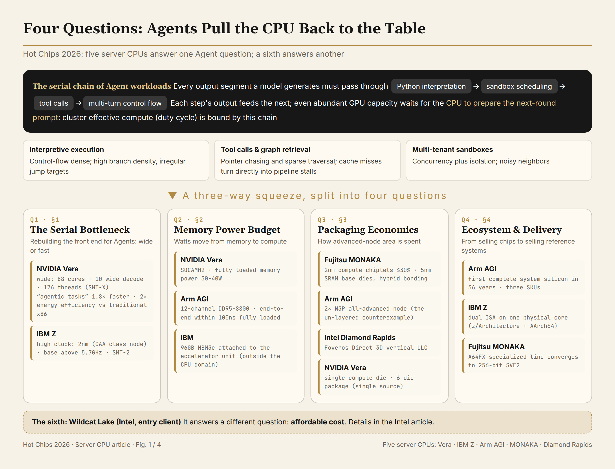
One. The Serial Bottleneck: Two Ways to Rebuild the Front End for Agents
Agent workloads squeeze CPU microarchitecture from three sides. Interpreted execution is control-flow-dense, with high branch density and irregular targets; tool calls and graph retrieval bring pointer chasing and sparse traversal, and once cache hit rates fall, the pipeline starts waiting for data; multi-tenant sandboxes add an isolation requirement on top. Against such workloads the answers split into two routes: widen the front end, or raise the clock.
Vera is the complete answer on the wide route, and the only CPU that says out loud it was designed for agents. It has 88 self-designed Olympus cores (Armv9.2, not the stock Neoverse) and 176 threads (SMT-X). At the microarchitecture level, the 10-wide physical decode front end swallows the control-flow-dense instruction stream; the homegrown neural branch predictor calls the branches right amid the irregular jumps; the graph prefetcher watches array-indirection access patterns and moves graph nodes into the cache ahead of time — graph traversal and pointer chasing are precisely the memory accesses that hurt pipelines most in agent workloads. Each core also carries six 128-bit SVE2 vector pipelines (with dual crypto units), supporting FP8. For microarchitecture numbers we accept only two kinds of sourcing: the July whitepaper, and what Hot Chips itself disclosed (the latter amounts to two or three items, one being the SPEC 2017 comparison for Spatial SMT).
Spatial SMT is the most distinctive design in this CPU. Conventional SMT has two threads dynamically contending for the same front end and issue queues; multi-tenant agent sandboxes become noisy neighbors, and tail latency wobbles. As an analogy: conventional SMT is two families sharing one kitchen and bathroom; Spatial SMT walls it off, each with its own set. In single-thread mode, all resources go to one thread for peak single-core performance; in dual-thread mode, the decode front end, issue queues, and execution units are physically partitioned, each thread with its own path. The other half of isolation is security: Vera is the industry's first confidential-computing CPU to enable TDISP for coherent devices (official claim), with the hardware trust boundary extending from the CPU to GPUs on NVLink. Wherever the orchestration layer extends, the security boundary follows.
NVIDIA's scorecard: "agentic tasks" complete 1.8x faster with 2x the efficiency versus traditional x86; in the SPEC CPU 2026 official proxy estimate, 2P scores 925 against 898 for AMD Turin. These are marketing figures; independent verification is still pending.
IBM takes the other route: frequency. It pushes the base clock above 5.7GHz on 2nm (a GAA-class node), with SMT-2. Wide bodies trade area for instructions per cycle, high clocks trade per-cycle work for cycles per second. The two routes point to one judgment: the serial chain is once again the server CPU's first constraint.
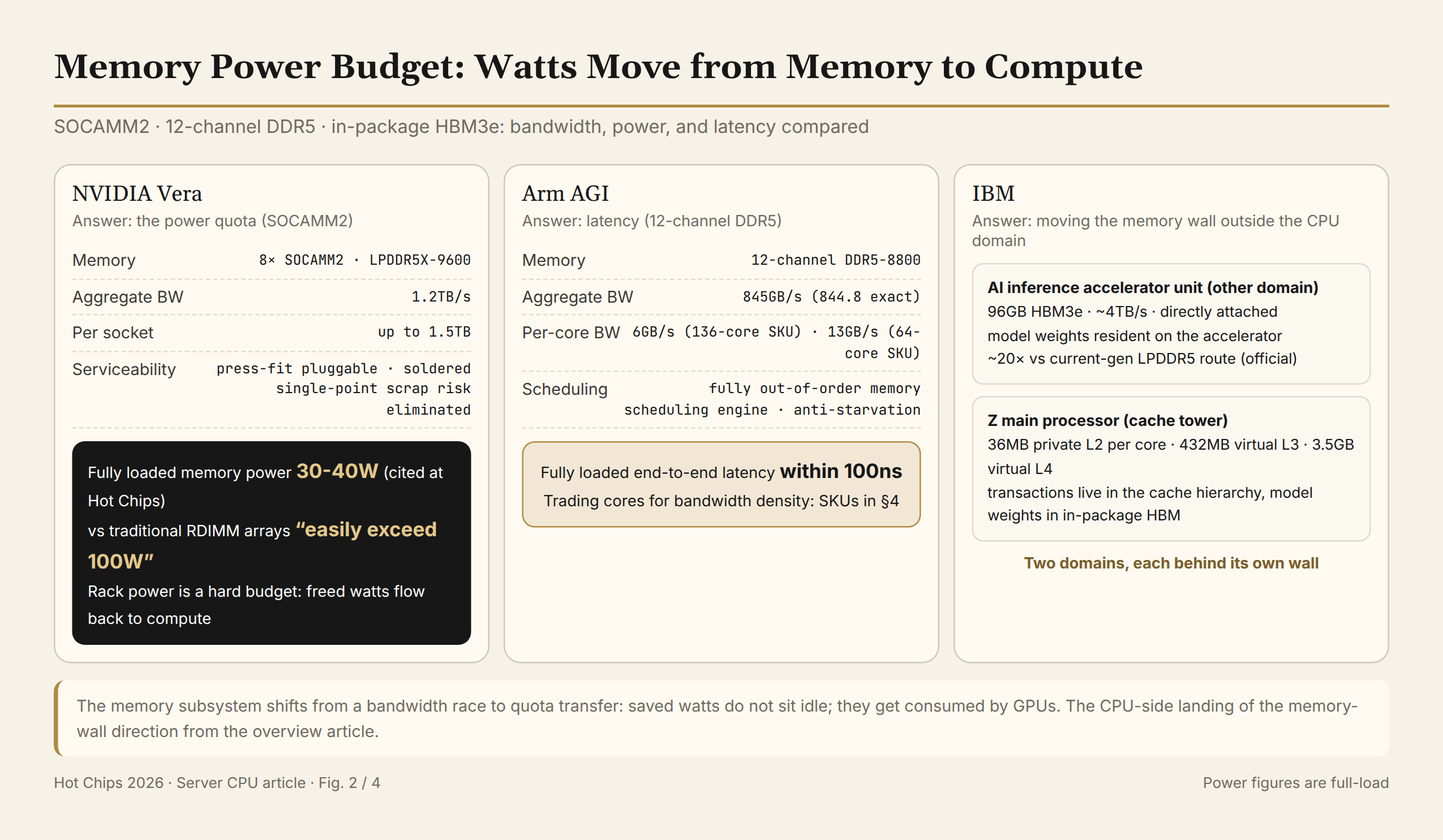
Two. The Memory Power Budget: Power Moves from Memory to Compute
In Vera's memory design, what matters more than capacity and bandwidth is power. Eight SOCAMM2 modules running LPDDR5X-9600 deliver 1.2TB/s of aggregate bandwidth and up to 1.5TB per socket, at a full-load memory power of just 30-40W (as quoted at Hot Chips); a conventional RDIMM array typically exceeds 100W by comparison. Rack power is a hard budget, and saved power does not sit idle; the GPUs take it directly. The socketed, field-replaceable design closes the remaining operations gap: LPDDR efficiency and server-memory maintainability are finally attainable together, and the single-point scrap risk of board-mounted soldering is eliminated.
Arm's answer is latency. Twelve channels of DDR5-8800 deliver a total of 845GB/s of aggregate bandwidth (844.8 exact), with loaded end-to-end access latency held under 100ns, backed by a fully out-of-order memory scheduling engine and anti-starvation mechanisms. The 6GB/s per core is the 136-core SKU number; the 64-core SKU trades core count for bandwidth density, reaching 13GB/s per core.
Intel's Diamond Rapids offers a fourth approach: push the conventional route to its limit. With 16 memory channels, it stacks bandwidth and capacity to the scale rack orchestration demands. Vera left this route to save power; Intel stayed on it for bandwidth: the two choices run in opposite directions (the deployment details of Diamond Rapids are in the Intel piece).
IBM moves this constraint outside the CPU domain. 96GB of HBM3e at roughly 4TB/s sits directly attached to the second-generation AI inference accelerator chipset, with model weights resident on the accelerator — officially, roughly 20x the bandwidth of the current generation's LPDDR5 route. Those figures belong to the accelerator chipset, not with the Z processor's own memory; the processor side keeps its own high-bandwidth cache hierarchy: 36MB of private L2 per core, 432MB of virtual L3, 3.5GB of virtual L4. Transaction data turns inside the cache hierarchy while model weights sit in in-package HBM: two domains, each independent.
The memory subsystem's competitive dimension has therefore changed: no longer peak bandwidth, but bandwidth per watt. The memory-wall direction from the overview reaches this point on the CPU side.
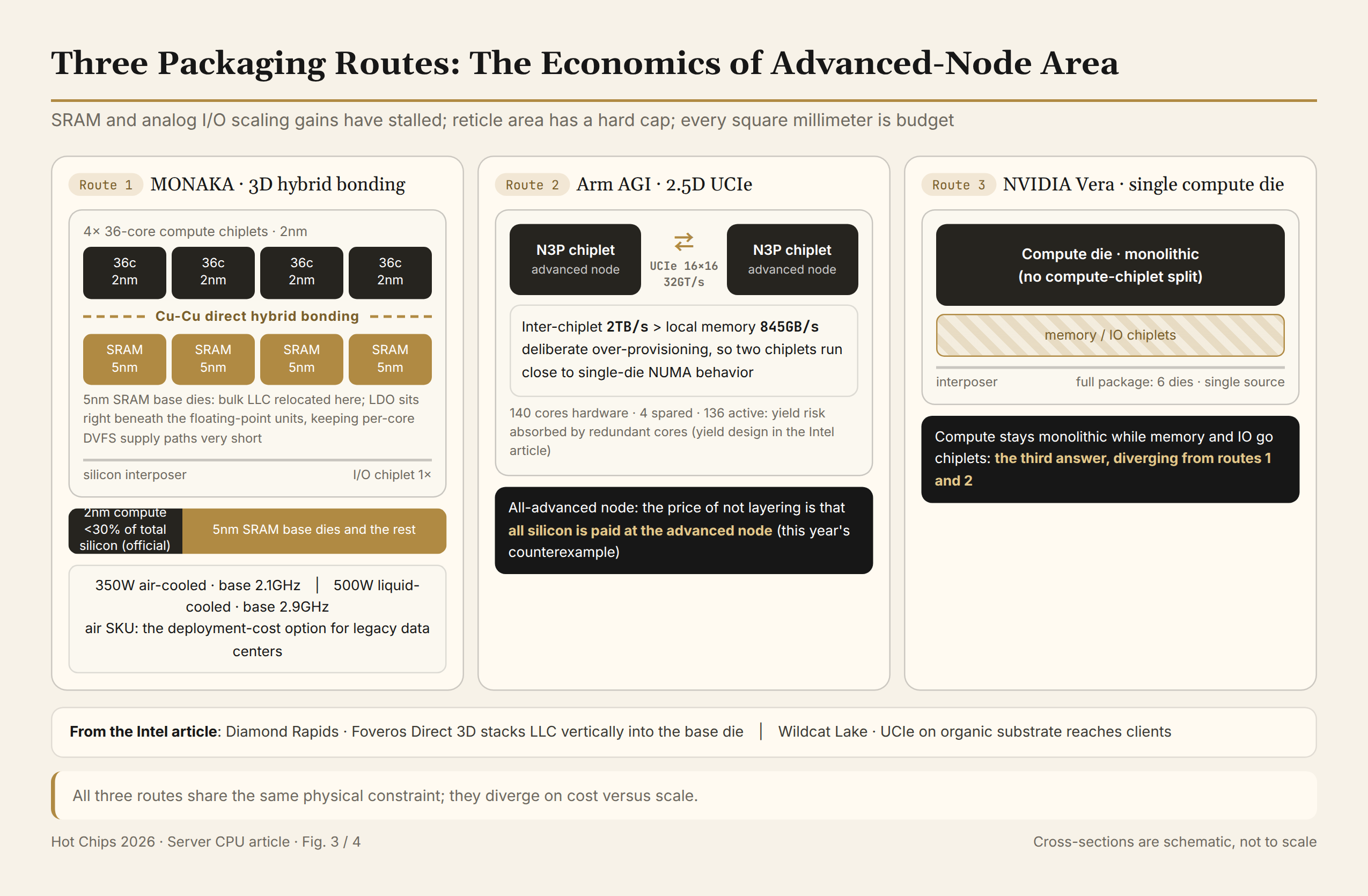
Three. Packaging: Three Ways to Spend Advanced-Node Area
The physical constraints on packaging are clear: SRAM and analog I/O scaling gains have stalled at advanced nodes, and reticle area is capped. Every square millimeter of advanced process is budget, and three companies spend it three ways.
MONAKA does this math in public. The 2nm compute chiplets are held under 30% of total silicon area (official figure), the bulk LLC is carved out entirely onto 5nm SRAM base dies, and Cu-Cu hybrid bonding stacks them in 3D. The structure: four 36-core compute chiplets bonded onto four SRAM base dies, plus one I/O die on a silicon interposer. Tucked into the layout is a detail worth noting: LDOs, the analog circuits that scale worst at 2nm, sit in the SRAM base die directly beneath the floating-point units, keeping per-core DVFS supply paths extremely short. MONAKA offers two SKUs: a 350W air-cooled version at a 2.1GHz base clock and a 500W liquid-cooled version at 2.9GHz; the air version is the deployment-cost option for existing machine rooms.
Arm's AGI is the counter-example that doesn't layer. Both N3P chiplets are all advanced node, no process split, with yield risk absorbed by redundant cores (140 cores in hardware, 4 held back, 136 delivered; the yield design is in the Intel piece). The inter-chiplet link is deliberately generous: a UCIe 16x16 macro array running at 32GT/s, 2TB/s aggregate, intentionally above local memory bandwidth (845GB/s), letting the dual chiplets deliver near-monolithic NUMA performance. Flattening cross-die overhead with interconnect above local bandwidth; over-provisioning is itself the design language.
Vera takes the third route: a monolithic compute die with no compute-chiplet split (the full package is six dies on an interposer; so far only one outlet has recorded this detail).
Intel's two parts cover the other two routes. Diamond Rapids pushes the 3D route onto the server mainline: Foveros Direct 3D direct bonding lifts per-unit-area die-to-die bandwidth an order of magnitude above conventional bumps, with compute dies and cache/IO dies each built on the fitting process, then vertically composed into 256 cores and 1.28GB of LLC; loading the LLC into a mature-process base tile is precisely the Intel edition of the layered route. Wildcat Lake covers the low-cost end: UCIe organic substrate into clients, the open interconnect serving both high-bandwidth advanced packaging and cost-sensitive traditional substrates, with an entry-level 2P+4E configuration (NPU 17 TOPS, official claim) aimed at a different need. The full details of both are in the Intel piece.
All three routes face the same physical constraint and diverge on cost-versus-scale trade-offs. AGI shows the price of not layering: every square millimeter pays advanced-node rates.
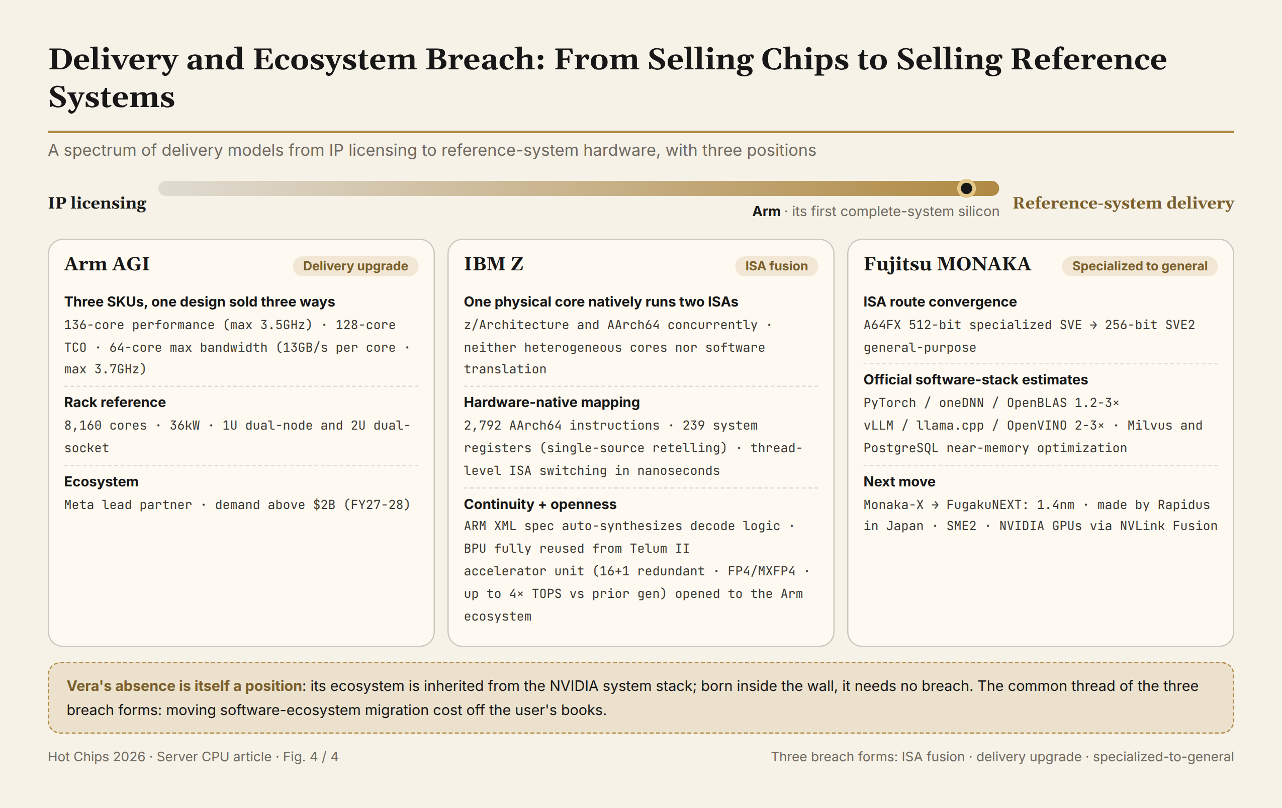
Four. Delivery and the Ecosystem Wall: From Selling Chips to Selling Reference Systems
For the first time, Arm builds its own whole-machine chip, and the delivery form changes with it: from selling IP licenses to delivering a reference system validated on N3P and UCIe packaging. The SKU sheet is itself a market judgment: 136 cores for performance, 128 for TCO, 64 for maximum bandwidth at 13GB/s per core, one design covering three market segments. "Arm AGI, 136 cores at 3.7GHz," a widely circulated reading, we checked against Arm's official SKU sheet: it splices two SKUs. The 136-core SKU tops out at 3.5GHz, and 3.7GHz belongs to the 64-core SKU. On the ecosystem side, Meta is the lead partner, and Arm management disclosed demand above $2 billion (FY27-28 basis); the official rack reference is 8,160 cores in a 36kW rack, in both 1U dual-node and 2U dual-socket chassis.
The most thorough form of ecosystem breakthrough appears at IBM. A single physical core natively executes two instruction sets, with z/Architecture and AArch64 running concurrently, not big.LITTLE and not software translation. The ARM XML specification is automatically synthesized into decode logic, with 2,792 AArch64 instructions and the 239-system-register mapping executed natively in hardware (the 239 figure has appeared in only one outlet's account), and thread-level ISA switching completes in nanoseconds. There is direct evidence of engineering continuity: the branch prediction unit is reused wholesale from Telum II. So CICS and DB2 transaction code that has run on z/OS for decades, and cloud-native Arm containers, can execute in the same physical core, sharing the same 36MB of L2 — keeping the Z assets or entering the Arm ecosystem, that either/or choice has been canceled by hardware. The AI accelerator chipset (16+1 redundant, FP4/MXFP4, up to 4x the TOPS of the previous generation) opens to the Arm ecosystem as a Linux platform device, with latency close to native Z.
Fujitsu's approach is contraction. A64FX's 512-bit special-purpose SVE converges to the general 256-bit SVE2 route, and the supercomputer special becomes an enterprise generalist. Official software-stack estimates: PyTorch, oneDNN, and OpenBLAS gain 1.2 to 3x; vLLM, llama.cpp, and OpenVINO gain 2 to 3x; Milvus and PostgreSQL get near-memory optimization; the CCA sovereignty platform shapes confidential computing into what the European market needs. The follow-on roadmap is already announced: Monaka-X points to FugakuNEXT, on a 1.4nm process, built by Rapidus in Japan, adding SME2, and connecting to NVIDIA GPUs via NVLink Fusion.
Vera's name is absent from the delivery list. The absence itself explains its position: its ecosystem comes directly from the NVIDIA system stack; it faces no ecosystem wall, so no breakthrough is needed.
ISA fusion, delivery upgrade, special-to-general: the three forms of breakthrough share exactly one thing, moving software-ecosystem migration cost off the user's side.
Five. Summary and Judgments
Five server CPUs face the same agent workload. The serial bottleneck makes them rebuild the front end, the memory power budget makes them re-allocate power, advanced-node area makes them re-price packaging, and the ecosystem barrier makes them redraw delivery boundaries. With this, all four directions from the overview are complete. The key specs and question placements of the six chips are summarized below.
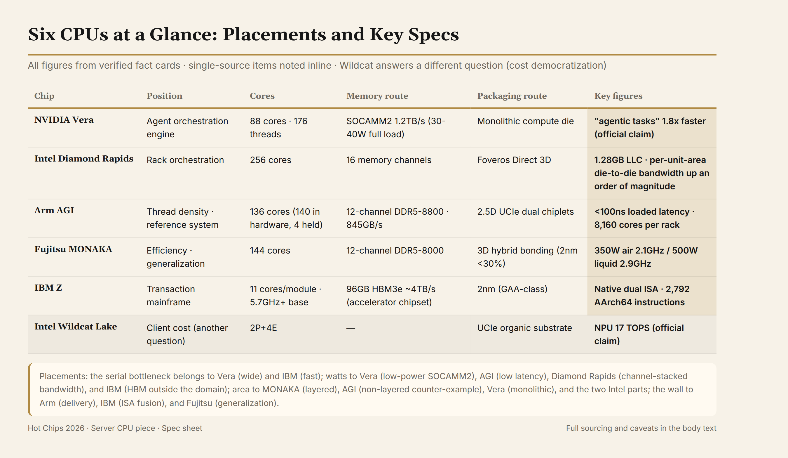
Judgment one: agent workloads re-diverge CPU microarchitecture, wide versus fast, but only Vera is designed end to end for agents, from microarchitecture to security boundary; the rest are partial answers. Verification points: Arm AGI's actual deployment announcements and the first shipment figures once Vera CPUs are sold standalone, the same events that verify the Intel piece's triangle judgment; the microarchitecture-specific points are IBM's dual-ISA rollout pace and whether second-generation products continue the divergence.
Judgment two: the memory power budget transfer will become the design language of AI-factory servers within one to two generations. SOCAMM2 presses full-load memory power to the 30-40W class, and the freed hundred-odd watts flow straight back to compute. Verification point: whether the next-generation Xeon and AGI's follow-on SoC (roadmap committed, no timeline given) follow the LPDDR route.
Judgment three: packaging layering will move from engineering practice to industry discipline. MONAKA's "advanced-node area under 30%" is the only explicitly stated official figure this year, and Diamond Rapids' 3D stacking walks the same road; AGI's all-advanced-node is the ready counter-example and its own verification point — if its second generation is forced into layering, the discipline holds. Verification point: node-area ratios of chips announced in 2027.
The four questions are answered, and the CPU is back at the table. What comes next is each vendor's second-generation parts. We will keep watching four things: the AGI deployment announcement, Vera CPU shipment figures, whether IBM's dual ISA reaches the LinuxONE line, and the final specs of Monaka-X and FugakuNEXT (FugakuNEXT slated to run around 2030).