June 23, 2026, ISC 2026, Hamburg — the new TOP500 list drops: China's LineShine (灵晟) hits 2.19 EFLOPS FP64, becoming the world's first supercomputer to sustain over 2 EFLOPS. 47,000 CPUs, zero GPUs, and a fully domestic stack from processor to interconnect.
Meanwhile, the four other Exascale systems in the TOP500 top ten — El Capitan, Frontier, Aurora, and JUPITER — all run CPU+GPU heterogeneous architectures. Fugaku, the previous pure-CPU champion, has fallen to sixth place, and Japan has announced that its next-generation Fugaku-NEXT will pivot to ARM CPU + NVIDIA GPU heterogeneity.
Is the pure CPU route at a dead end, or has a new door just opened?
LineShine offers an unprecedented analytical sample: it is the most powerful pure-CPU supercomputer ever built, and three arXiv papers document real-workload performance data in detail. By tearing it down — CPU microarchitecture, interconnect network, end-to-end software path, and the empirical evidence from those three papers — we can assess where this route stands today and how much room it has left to scale.
I. The LX2 Processor: Fitting 304 Cores Into a Known Die Area
1.1 Process Node and Die Area Estimation
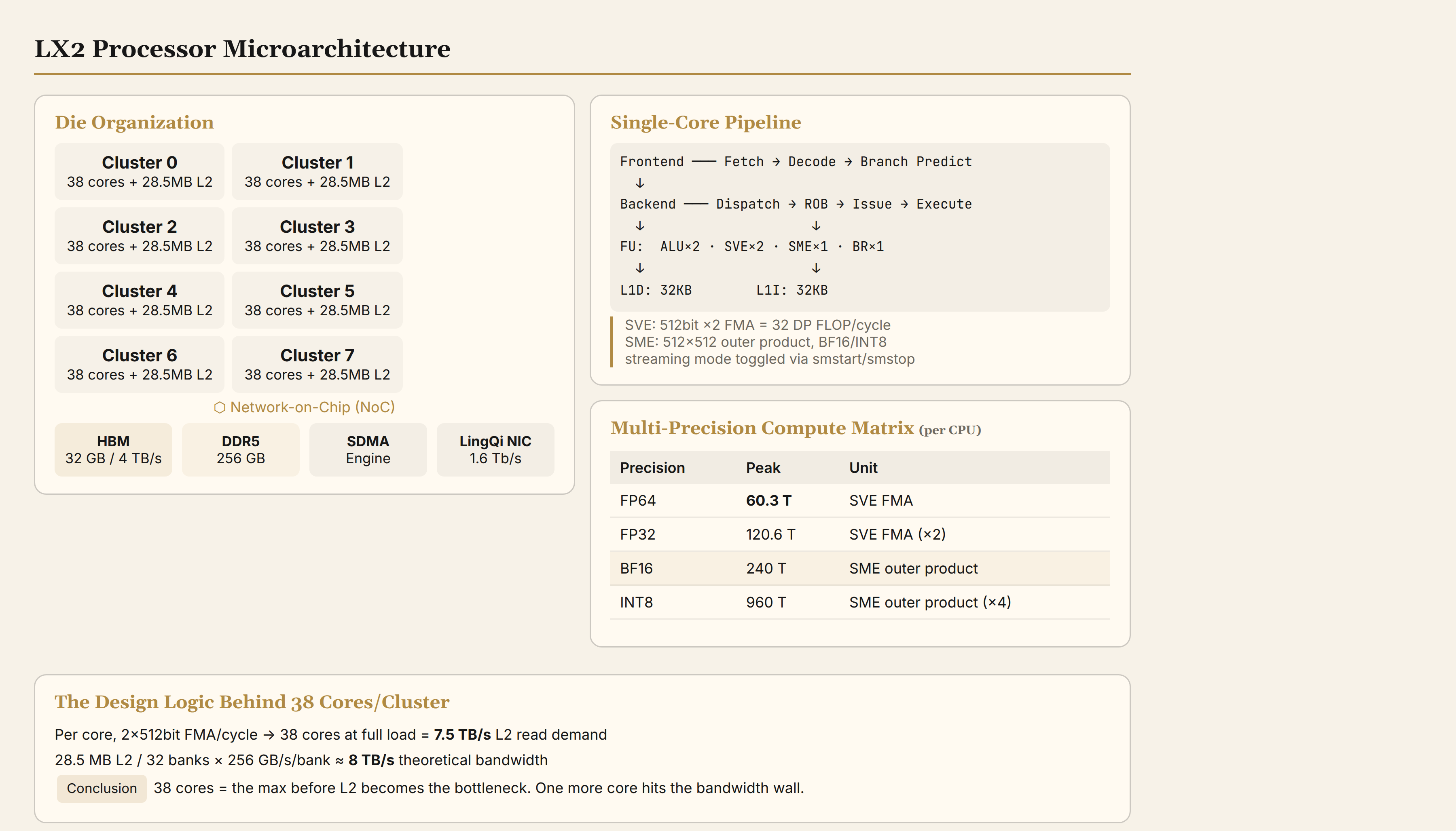
The heart of LineShine is the LX2 processor: 304 cores, ARMv9 architecture, 1.55 GHz base frequency, and 32 GB of integrated HBM per CPU (4 TB/s).
The process node is not publicly disclosed. Working from available public information, we can constrain the estimate:
Reference point 1: Fujitsu A64FX. TSMC 7nm, 48 cores (including 4 helper cores) + 4 HBM2 controller groups, die area approximately 480 mm², 8.786 billion transistors. That works out to roughly 10 mm² per core (including prorated L2 and controllers).
Reference point 2: ARM Neoverse V2. Physical implementation on TSMC 5nm yields approximately 2–3 mm² per core (including 1 MB private L2). On 7nm, Neoverse N2 is about 3–4 mm² per core.
LX2's area constraint. If built on SMIC 7nm (the most likely node for domestic HPC silicon), the transistor density is approximately 90–100 MTr/mm² (N+1 tier), below TSMC N7's 91 MTr/mm² and N5's 173 MTr/mm². LX2's 304 cores on a single die, at 3–4 mm² per core (7nm-class core + prorated L2), would require 900–1200 mm² for core logic alone. Add 8 HBM controller groups, the LingQi NIC, DDR5 controllers, SDMA engines, and I/O PHYs, and total die area reaches 1400–1800 mm².
The reticle limit for 7nm lithography is 858 mm². A single die cannot hold this.
Conclusion: LX2 is almost certainly a chiplet design. The most likely configuration is 2 compute chiplets (each with 4 clusters × 38 = 152 cores, approximately 600–700 mm²) plus 1 I/O die (HBM controllers, DDR5 controllers, NIC, SDMA). This mirrors the AMD Zen chiplet strategy — advanced process for compute dies, mature and cheaper process for the I/O die.
The chiplet design has direct performance implications. Communication between the 4 clusters within the same chiplet has low latency (shared L2 or ring), while cross-chiplet communication between the other 4 clusters must traverse the I/O die, incurring higher latency. This creates a two-level NUMA hierarchy:
| Level | Scope | Latency Characteristic |
|---|---|---|
| L2 local | Same cluster, 38 cores | ~15–20 cycles |
| Die local | Same chiplet, 4 clusters | ~30–50 cycles |
| Cross-die | Across chiplets, 4 clusters | ~80–150 cycles |
| Cross-CPU | Other LX2 in the node | ~200–400 ns |
| Cross-node | LingQi network | ~1–5 μs |
This NUMA hierarchy directly affects MPI process pinning strategy — communication-intensive processes should be co-located on the same chiplet.
1.2 Microarchitecture: Benchmarked Against ARM Neoverse V2
LX2's microarchitecture parameters are undisclosed. But the ARMv9 architecture specification and ARM's in-house reference cores (Neoverse V2/V3) provide a reasonable basis for inference. Neoverse V2 is ARM's flagship core targeting HPC and cloud, and it is the closest publicly known ARMv9 core to LX2's positioning.
| Parameter | Neoverse V2 (public) | LX2 (inferred) |
|---|---|---|
| Decode width | 5–6 instructions/cycle | Same class |
| ROB depth | 320+ | Same class |
| Physical registers (INT/FP) | 288/256 | Possibly larger (HPC workloads) |
| SVE vector width | 128/256/512 bit | 512 bit (confirmed) |
| SME | None | Yes (key LX2-exclusive extension) |
| L2 cache | 1–2 MB private per core | 28.5 MB shared per cluster (different design) |
The two most significant divergences between LX2 and Neoverse V2:
Difference 1: Fundamentally different L2 architecture. Neoverse V2 uses private per-core L2 (1–2 MB). LX2 uses a shared L2 per cluster of 38 cores (28.5 MB). Shared L2 provides large aggregate capacity (8 × 28.5 = 228 MB vs. 304 × 1 = 304 MB — comparable totals, but the shared model lets cores within a cluster reuse data loaded by their neighbors). The tradeoff: 38 cores contending for the same L2 banks and bandwidth. Earlier analysis showed that 38 cores at full FMA utilization demand approximately 7.5 TB/s of L2 bandwidth, while 28.5 MB / 32 banks × 256 GB/s/bank ≈ 8 TB/s — right at the limit. 38 cores is the maximum this L2 configuration can sustain.
Difference 2: SME integration. Neoverse V2 does not include SME (ARM plans to integrate it in the V3 generation). LX2 integrates SME independently — requiring a dedicated matrix execution pipeline in the core microarchitecture, a 2D accumulator register file (ZA tile), and streaming mode state-switching logic. This additional hardware occupies roughly 15–25% of the core area.
If LX2 derives from a V2 base, the single-core area with SME integrated would be approximately 3.5–5 mm² (7nm). If designed from scratch, the area difference depends on how the design team rebalanced the front-end and back-end — they might reduce integer ALU count to free area for SME.
1.3 SME: Matrix Acceleration on a CPU
SME (Scalable Matrix Extension) is an instruction set extension in the ARMv9 architecture designed for matrix computation. It introduces a new execution mode — streaming SVE mode — in which the processor uses a dedicated 2D accumulator (ZA tile) to perform outer product operations, completing a partial matrix multiply in a single cycle.
Each LX2 core's SME pipeline can complete one 512×512 bit outer product accumulation per cycle in BF16. At 304 cores × 1.55 GHz, this yields 240 TFLOPS BF16. By comparison, Neoverse V2 at the same frequency has no SME — its BF16 compute capability is zero without SME (it can only do BF16 FMA via SVE, which is 4–8× less efficient).
The SME programming model requires care. Entering streaming mode uses the smstart instruction; exiting uses smstop. The switching cost is undisclosed, but from ARM architecture specifications we can infer approximately 20–100 cycles. This makes frequent switching between SVE and SME within a single kernel uneconomical — ideally, a kernel runs entirely in SME mode (GEMM) or entirely in SVE mode (element-wise operations). The "asymmetric SME-GEMM" scheduling strategy described in the D2AR paper confirms this: SME and SVE usage is not a balanced mix, but rather SME-primary with SVE filling gaps in the SME pipeline's schedule.
1.4 Memory Hierarchy
LX2's memory subsystem has three physical tiers:
L1/L2 cache. Each core has 32 KB L1-I + 32 KB L1-D; each cluster has 28.5 MB shared L2. The 228 MB total L2 (across 8 clusters) sits in the mid-range for HPC CPUs — Intel Sapphire Rapids has 2 MB L2 per core (56 cores = 112 MB), AMD Genoa has 256–384 MB shared L3. LX2's shared L2 design achieves high reuse within a cluster, but cross-cluster cache coherence requires cross-chiplet communication.
HBM. 32 GB, 4 TB/s bandwidth. The bandwidth density is 125 GB/s per GB — far higher than H100's 42 GB/s per GB (80 GB / 3.35 TB/s). This "small but fast" design suits scientific computing with frequent access to modest-sized data batches, but 32 GB is a hard constraint for AI training (a 6.3B parameter model's training state requires approximately 50 GB).
DDR5. Up to 256 GB, bandwidth approximately 200–400 GB/s. Used as an overflow tier for HBM — the SDMA engine shuttles data between HBM and DDR5 on demand.
SDMA (Software-defined DMA) engine. Located in the I/O die, responsible for data movement between HBM and DDR5. The D2AR paper describes its operation: based on operator type (compute-bound vs. memory-bound) and the lifetime of intermediate results, the runtime dynamically decides which data resides in HBM and which gets evicted to DDR5. The scheduling granularity is page-level (4 KB). This is a hardware-assisted tiered memory management mechanism — not transparent OS-level swap, but explicit application control through a driver interface.
1.5 What Multi-Precision Compute Physically Means
| Precision | Per-CPU Peak | Compute Unit | Use Case |
|---|---|---|---|
| FP64 | 60.3 TFLOPS | SVE FMA | Scientific computing (CFD, weather, molecular dynamics) |
| FP32 | 120.6 TFLOPS | SVE FMA | uMLIP training (quantum accuracy required) |
| BF16 | 240 TFLOPS | SME outer product | AI training |
| INT8 | 960 TOPS | SME outer product | AI inference |
Compared to H100: FP64 34 TFLOPS (excluding Tensor Cores), BF16 989 TFLOPS. LX2 dominates H100 in FP64 (1.8×) but reaches only 24% of H100's BF16.
The physical implication: LX2's die area allocates heavily to SVE vector units and lightly to SME matrix units. This is a scientific-computing-first silicon allocation — more area for FP64 vector operations, less for matrix multiply. The exact opposite of GPU area allocation (GPUs devote most die area to Tensor Cores).
If AI workloads continue to grow and scientific computing's share declines, this allocation would need to flip — but a flipped LX2 becomes "a GPU with an ARM CPU attached," losing the programming simplicity that defines the pure CPU route.
II. From Node to System
2.1 Compute Node
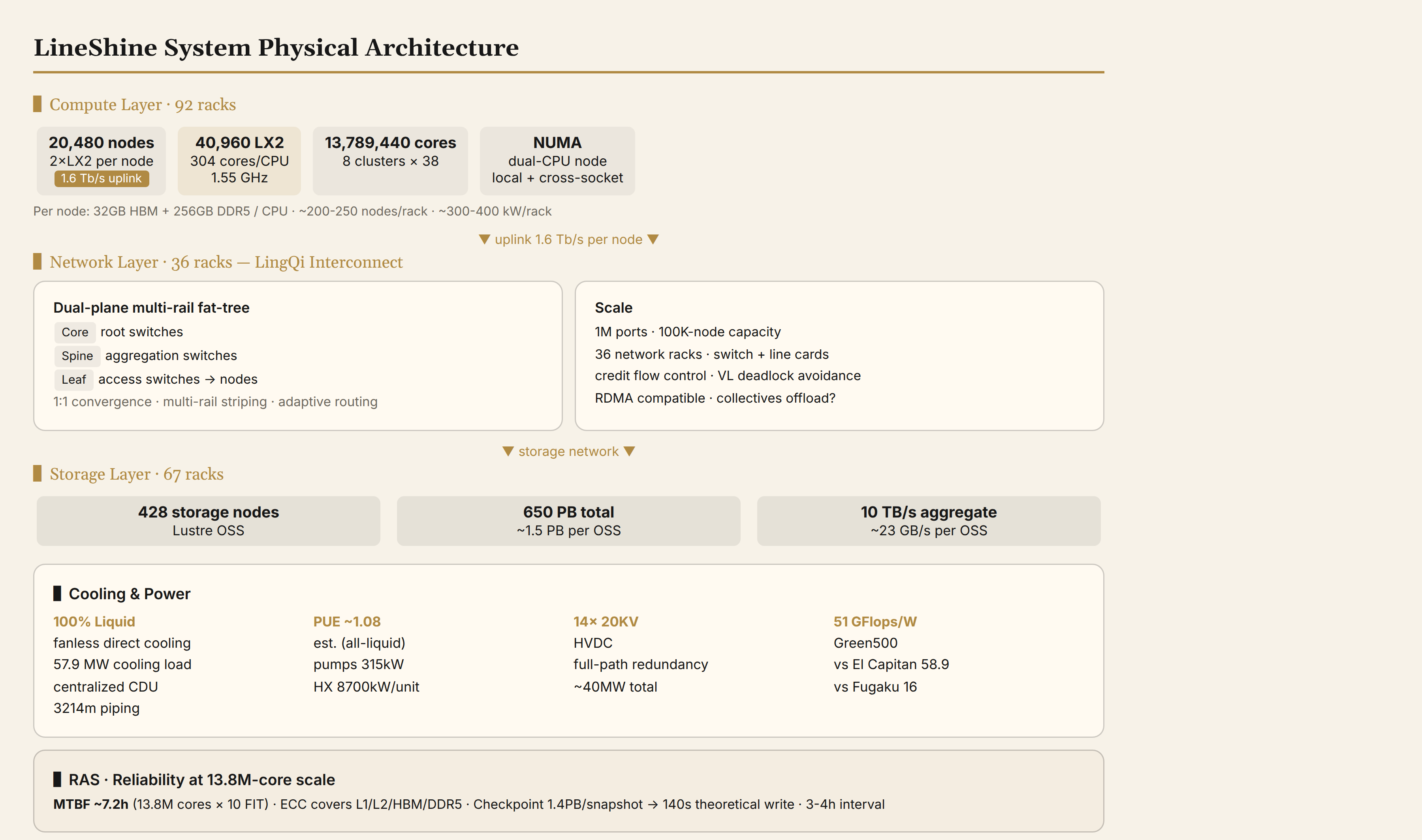
Each compute node carries 2 LX2 processors. The coherence interconnect between the two CPUs is undisclosed — it could be an ARM CMN (Coherent Mesh Network) based mesh, or Huawei's UB (Universal Bus) technology — analyzed below.
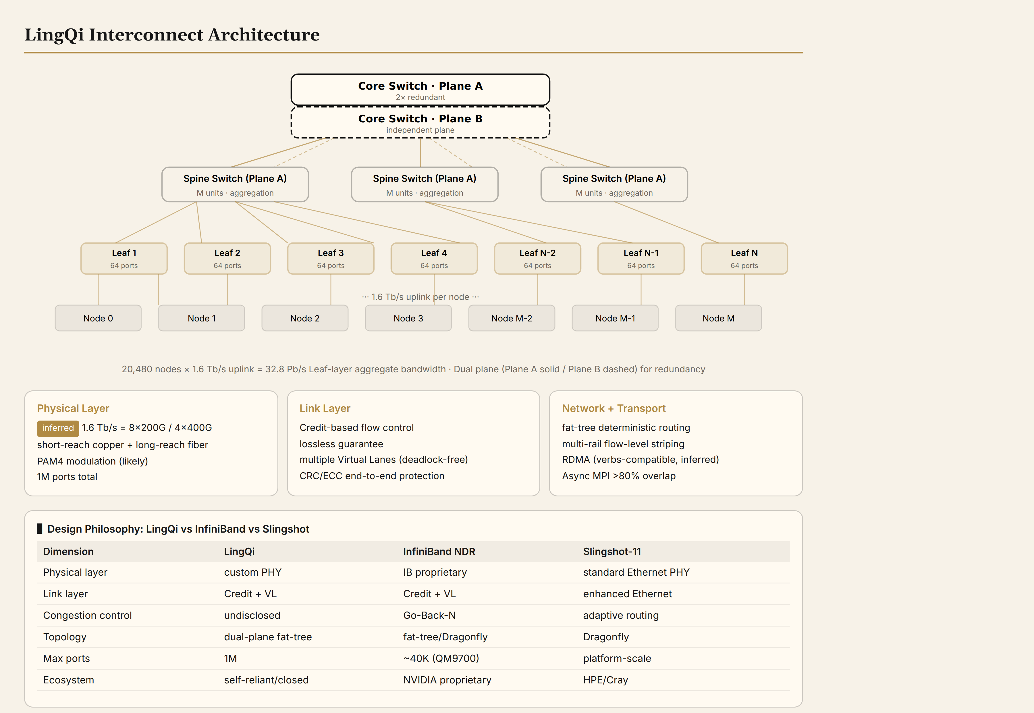
The node's uplink bandwidth is 1.6 Tb/s. This means both LX2 processors share a single network egress — even though internal HBM bandwidth is abundant, cross-node communication is bottlenecked by this 1.6 Tb/s uplink.
2.2 Rack and Physical Scale
| Component | Quantity | Key Parameters |
|---|---|---|
| Compute racks | 92 | ~200–250 nodes/rack, estimated 300–400 kW/rack |
| Network racks | 36 | LingQi switches, line cards |
| Storage racks | 67 | 428 storage nodes, 650 PB, 10 TB/s aggregate bandwidth |
| Cores | 13,789,440 | Used for HPL benchmark |
| Power | ~40 MW | |
| Cooling | 100% liquid-cooled | 57.9 MW cooling load, estimated PUE 1.05–1.15 |
| Efficiency | 51 GFLOPS/W | vs. El Capitan 58.9, vs. Fugaku 16 |
51 GFLOPS/W means each watt of electrical power produces 51 GFLOPS of sustained FP64 compute. El Capitan's 58.9 GFLOPS/W is 15% higher — the gap stems primarily from process technology (TSMC 5nm vs. domestic 7nm-class) and architecture (MI300A APU's higher GPU compute density).
The liquid cooling system was designed by China Zhongyuan, using a centralized CDU architecture with 3,214.7 meters of secondary piping, 315 kW circulating pumps, and 8,700 kW per-plate heat exchangers. 14-route 20 kV high-voltage DC power distribution.
2.3 LingQi Interconnect: The Huawei UB Hypothesis
LingQi (灵启) is LineShine's self-developed interconnect network: a dual-plane multi-rail fat-tree topology, 1.6 Tb/s per node, with stated scaling capability to 1 million ports.
Public materials do not describe LingQi's protocol stack details. But from known information, there is a high probability that LingQi is technically linked to Huawei's UB (Universal Bus) high-speed interconnect technology:
Clue 1: LineShine's LX2 is closely related to the Huawei Kunpeng ecosystem. Launch events mentioned Huawei's participation, and LineShine's software stack interfaces with Kunpeng. Huawei has mature supernode interconnect technology internally — LingQu software (kernel layer) + hardware interconnect (including UB physical layer). LineShine's "LingQi" and "LingQu" naming even aligns with Huawei's LingQu system.
Clue 2: The 1.6 Tb/s per-node bandwidth matches the order of magnitude of Huawei's supernode solution's node-level interconnect bandwidth. Huawei's HCCS (Huawei Cache Coherent System) interconnect used in Ascend clusters operates at similar bandwidth levels.
Clue 3: LineShine's design-to-deployment timeline (approximately 3–4 years) overlaps with the maturation period of Huawei's UB technology. Designing LingQi entirely from scratch within this timeframe would be insufficient.
Hypothesis: LingQi is likely a hybrid of Huawei's UB physical layer plus a custom upper-layer protocol (MPI adaptation, collective communication optimization) developed by the Shenzhen Supercomputing team. The physical and link layers reuse Huawei technology; the network and transport layers are customized for HPC workloads.
Analytical implication: If this holds, LingQi is not "a network built from zero by one team" but "a supercomputing-scale extension of Huawei's commercial interconnect technology." This means LingQi's reliability benefits from Huawei's large-volume hardware validation, while the custom protocol layer's maturity needs to be assessed through operational data.
Port count estimation: 20,480 nodes × multiple ports per node (assuming 4 rails, each at 400 Gb/s = 1.6 Tb/s). Two-layer fat tree: the Leaf layer needs 20,480 access ports; assuming 64-port Leaf switches → 320 Leaf switches. The Spine layer provides uplinks for 320 Leaf switches → approximately 160–320 Spine switches. The Core layer connects the dual planes → approximately 80–160 Core switches. Total switches: approximately 560–800, total ports: approximately 700,000–1,000,000 — consistent with the publicly stated "1 million ports."
2.4 Storage
67 storage racks, 428 storage nodes, 650 PB total capacity, 10 TB/s aggregate bandwidth. Each storage node carries approximately 1.5 PB capacity and 23 GB/s bandwidth — a typical Lustre OSS (Object Storage Server) configuration. Whether burst buffers (NVMe caching layers) are deployed is undisclosed.
III. Software: From Code to SME Instructions
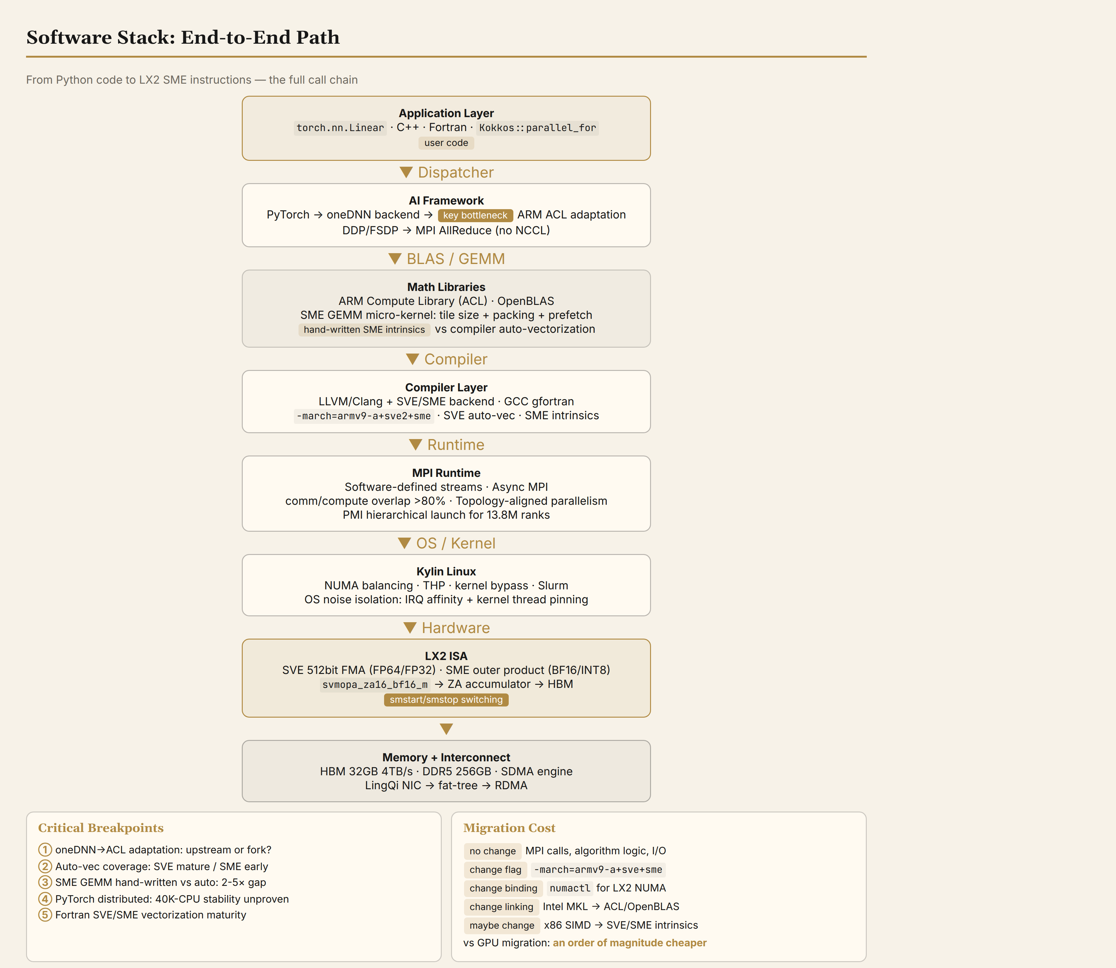
3.1 Compiler
LX2's compiler selection is undisclosed. The ARM HPC ecosystem offers LLVM/Clang or GCC, both supporting SVE auto-vectorization. SME compiler support is newer — LLVM mainline's full support for SME intrinsics and streaming mode was merged progressively during 2024–2025.
If LX2's toolchain is based on an earlier LLVM fork, SME auto-vectorization coverage will lag behind the latest mainline. In practice, high-performance kernels almost certainly require hand-written SME intrinsics — compiler-generated code on complex kernels may run 2–5× slower than hand-tuned code.
A typical SME outer product matrix multiply kernel:
// SME outer product: C += A × B (BF16 → FP32 accumulate)
__arm_new("za")
void sme_gemm(bfloat16_t *A, bfloat16_t *B, float *C, int M, int N, int K) {
    svbool_t pg = svptrue_b16();
    for (int k = 0; k < K; k++) {
        svbfloat16_t va = svld1_hor_bf16(pg, &A[k * M]);
        svbfloat16_t vb = svld1_ver_bf16(pg, &B[k * N]);
        svmopa_za16_bf16_m(pg, ZA0, va, vb);  // 外积累加到 ZA
    }
    svst1_hor_bf16(pg, C, svread_hor_za16_bf16(ZA0));  // 写回
}
svmopa_za16_bf16_m is the core instruction: it completes a 512×512 bit outer product accumulation in a single cycle. ZA is SME's dedicated 2D register array, managed separately from SVE's 1D vector registers z0–z31. After entering streaming mode, some of SVE's predicate functionality is restricted.
3.2 AI Framework Invocation Chain
The path from PyTorch to LX2 hardware:
torch.nn.Linear → PyTorch dispatcher → oneDNN ARM backend
→ ARM Compute Library (ACL) GEMM kernel → SME intrinsic/assembly
→ ZA accumulator → L2 → HBM
ARM Compute Library (ACL) is ARM's official open-source compute library, providing BLAS, CNN, and other kernels for ARM CPUs. Upstream ACL's optimized SME kernels were added progressively during 2024–2025. Whether LX2 uses upstream ACL directly or a custom fork is undisclosed — but the D2AR paper team implemented their own SME-GEMM optimization ("reuse-directed asymmetric" scheduling), suggesting that upstream ACL performance on LX2 was not ideal.
PyTorch can run training on ARM CPUs, but distributed training (DDP/FSDP) across 40,000+ CPUs is an open question — PyTorch's Gloo backend has known scalability bottlenecks at very large cluster sizes, making the MPI backend more viable but requiring customization.
3.3 MPI and Software-Defined Streams
LineShine's MPI implementation is most likely a customized version based on MPICH or OpenMPI, with the underlying transport adapted to the LingQi network via libfabric or UCX.
At 13.8 million ranks, collective communication algorithm choice directly impacts efficiency:
- AllReduce: Recursive doubling requires log₂(13.8M) ≈ 24 steps, each with global synchronization. The ring algorithm rotates data and is more bandwidth-friendly but higher latency. Under LineShine's fat-tree topology, ring physical paths can be optimized for minimum hop count.
- AlltoAll: The core operation in MoE routing. O(P²) messages across 40,000 ranks is the primary communication bottleneck. The "atom-type-aware communication compression" in the MatRIS-MoE paper directly compresses AlltoAll data volume.
Software-defined streams. Mentioned multiple times across the papers but never formally defined. From context, this models MPI communication operations as nodes in a directed acyclic graph (DAG), with the runtime executing independent communications in parallel according to topological order while CPU cores simultaneously execute compute kernels. The effect: compute-communication overlap exceeds 80% — meaning 80% of communication time that was originally serialized is now asynchronously hidden.
3.4 OS and Large-Scale Operations
Kylin Linux kernel. At the scale of 304 cores/CPU × 40,000 CPUs:
OS noise. Random scheduling of kernel threads (kworker, kswapd, timer interrupts) produces microsecond-level latency spikes. In globally synchronized MPI operations, the slowest process determines global performance. Mitigation requires interrupt affinity binding (routing all interrupts to dedicated cores) and kernel thread pinning.
Job launch. Launching an MPI job across 13.8 million cores via standard SSH-based startup takes minutes. HPC systems use PMI (Process Management Interface) hierarchical launch trees to keep latency in the seconds range.
Checkpointing. A full-system job's checkpoint data volume can reach PB scale. At 10 TB/s storage bandwidth, writing 1 PB takes approximately 100 seconds in theory — longer in practice due to concurrency contention and metadata operations. Checkpoint frequency must balance data safety against productive compute time.
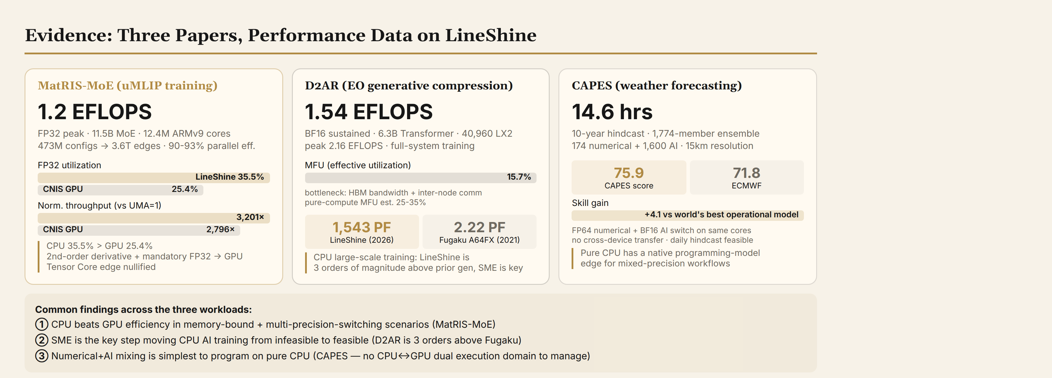
IV. Empirical Evidence: Probing the Limits of Pure CPU Clusters Through Three Case Studies
These three cases are not isolated paper validations — they are three probes, each testing the efficiency boundary of pure CPU architecture under different workload profiles. Read together, they reveal where LineShine's capability ceiling lies.
4.1 MatRIS-MoE: Why CPU Won Over GPU on Second-Derivative Training
MatRIS-MoE is a universal machine learning interatomic potential (uMLIP) model designed by the Institute of Computing Technology, Chinese Academy of Sciences. It uses neural networks to replace DFT (Density Functional Theory) for computing interatomic interaction forces. 11.5B parameter MoE architecture, 473 million configurations, 3.6 trillion interaction edges.
Understanding why CPU beats GPU on this workload requires unpacking three specific properties of uMLIP training:
Property 1: Second derivatives. LLM training only needs first-order gradients (∂L/∂θ). uMLIP training requires force matching — force is the negative of energy's first derivative with respect to coordinates (F = −∂E/∂X). The automatic differentiation framework must run backpropagation twice: first from energy to force, then from force to parameter gradients. This second pass computes "the gradient of the gradient" on the computation graph, with intermediate activations and memory consumption more than double that of first-order training.
GPU Tensor Cores are deeply optimized for first-order dense matrix multiplication — fixed tile shapes (16×16 or 32×32), predictable data prefetch patterns, highly regular pipeline scheduling. Second-order automatic differentiation produces entirely irregular computation graphs: each atom's force contribution depends on its neighbors' coordinates and energy, and neighbor counts and topology vary with the molecular system. This irregularity defeats Tensor Core tile prefetching, causing utilization to plummet.
CPU's SVE vector units have no tile shape constraint. Second-derivative intermediate activations are allocated directly in HBM and pulled into L2 by SDMA on demand. The programming model is identical to first-order training — just one more backward pass. This flexibility is an inherent advantage of CPU architecture.
Property 2: FP32 is a hard requirement. Quantum-accuracy simulation drops to BF16 would cause force prediction errors to accumulate until the molecular dynamics trajectory diverges. So uMLIP training must use FP32.
GPU FP32 compute comes in two tiers: "regular" FP32 (CUDA Cores, H100 approximately 67 TFLOPS) and Tensor Core FP32 (approximately 330 TFLOPS, but with strict tile constraints). The irregular graphs of second derivatives can only use the "regular" FP32 path, peaking at 67 TFLOPS.
LX2's SVE runs FP32 at native full speed: each core does 2 × 512-bit FMA per cycle = 16 FP32 operations. 304 cores × 1.55 GHz = 120.6 TFLOPS, which is 1.8× H100's "regular" FP32. This compute gap translates directly into a utilization gap.
Property 3: Edges are tokens, 3.6 trillion of them. GNN (Graph Neural Network) message passing operates along edges — edges are the fundamental compute unit. The memory access pattern of 3.6 trillion edges is completely irregular: adjacency lists are variable-length, and distance/angle triplets cannot be aligned and packed. This stands in sharp contrast to LLM tokens (fixed dimension, contiguous memory, regular batches). GPU Tensor Cores need regular batches to hit peak performance; irregular memory access severely degrades efficiency. CPU's out-of-order execution and hardware prefetching tolerate irregular access patterns far better.
Measured data. LineShine: 12.4M ARMv9 cores, FP32 peak 1.2 EFLOPS, utilization 35.5%. CNIS GPU cluster: 45K GPU cores, FP32 peak 1.0 EFLOPS, utilization 25.4%. A 10.1 percentage point gap. Normalized throughput: 3,201× the previous SOTA (UMA, 256 H200 GPUs training for 21 days).
Capability ceiling analysis. CPU's advantage here is structural — as long as uMLIP training requires second derivatives + FP32 + irregular data, CPU architecture is naturally matched to this workload. But this advantage has a precondition: sufficient HBM bandwidth. MatRIS-MoE's per-configuration data footprint is modest (local graphs of a few hundred atoms), so 32 GB HBM easily accommodates intermediate activations for multiple configurations. If future uMLIP models scale up — say from 11.5B to 50B+ — single-configuration activations may exceed HBM capacity, and SDMA scheduling becomes a bottleneck, eroding CPU's utilization advantage.
A second boundary: 35.5% FP32 utilization means 64.5% of time goes to non-compute work — communication, memory access, scheduling. At 12.4M core scale, communication overhead grows sub-linearly with core count (AllReduce's log steps, AlltoAll's O(P²) message count). If LineShine's scale doubled to 25M cores, communication's share could rise from the current ~10% to 15–20%, dropping FP32 utilization below 30%. LineShine's scale is near the sweet spot for pure-CPU uMLIP training — any larger, and communication overhead begins eroding efficiency.
4.2 D2AR: 32 GB HBM Is the AI Training Ceiling
D2AR is a remote sensing generative compression model from Tsinghua/Sun Yat-sen University. It trains a generative compressor on historical satellite archives to achieve 100× to 10,000× data compression. 6.3B parameter Dense Transformer, BF16 precision, trained across all 40,960 LX2 CPUs in the system.
Sustained performance: 1.54 EFLOPS. Peak: 2.16 EFLOPS. MFU: 15.7%.
The D2AR paper's Table 1 provides an excellent cross-comparison anchor. Placing it alongside large-scale GPU training data:
| System | Model | Scale | Precision | MFU | Sustained PFLOPS |
|---|---|---|---|---|---|
| MegaScale (A100) | 175B LLM | 12,288 GPU | BF16 | 55% | 2,166 |
| AxoNN (H100) | 60B LLM | 6,144 GPU | BF16 | 23% | 1,423 |
| ORBIT-2 (MI250X) | 10B Climate | 65,536 GPU | FP32 | ~16% | 4,100 |
| Fugaku (A64FX) | 7M Cosmology | 16,384 CPU | FP64 | ~2.0% | 2.22 |
| LineShine (LX2) | 6.3B EO | 40,960 CPU | BF16 | 15.7% | 1,543 |
This table is information-dense. Several numbers demand a pause:
LineShine's 1,543 PFLOPS is the all-time record for a CPU platform. Second-place Fugaku sits at 2.22 PFLOPS — a 695× gap. But Fugaku's model had only 7M parameters, FP64 precision, and no matrix acceleration. LineShine's 1,543 PFLOPS comes almost entirely from SME's BF16 matrix multiplication. Swapping Fugaku's A64FX for LX2 on the same model would yield an estimated 500–800 PFLOPS — the same order of magnitude.
15.7% MFU is low among large-scale training runs. MegaScale achieves 55% on GPUs — a 3.5× gap. But ORBIT-2 (climate simulation, FP32, GPU) also only reaches ~16% — nearly identical to LineShine. This tells us that 15.7% MFU is not solely a CPU architecture problem; it also reflects workload type (non-LLM vision model), precision choice, and communication patterns.
Decomposing the 15.7%. D2AR's end-to-end time breaks into four buckets:
-
SME compute (GEMM + attention): estimated 40–50% of time. Pure SME GEMM hardware utilization is limited by HBM bandwidth — at 4 TB/s bandwidth and 240 TFLOPS SME peak, each byte of data can only support ~60 GFLOPS of compute. If an operator's arithmetic intensity falls below 60 FLOP/byte, SME is memory-bound. Transformer attention layers at long sequence lengths have high compute density, but embedding and normalization layers have extremely low compute density, dragging down overall utilization.
-
Communication (AllReduce + AlltoAll): estimated 15–20%. The paper reports compute-communication overlap exceeding 80%, but the remaining 20% of serialized communication directly reduces MFU. Across 40,960 CPUs, one AllReduce takes approximately 24 steps (log₂(40960) ≈ 15, but effectively 20–25 steps due to fat-tree topology), each step hundreds of microseconds. AlltoAll's message count is O(P²) = O(1.7B); even at a few KB per message, total volume is in the terabytes.
-
SDMA memory scheduling: estimated 15–20%. The 6.3B parameter training state is approximately 50 GB (parameters 12.6 GB + Adam optimizer 37.8 GB + activations), exceeding a single LX2's 32 GB HBM. SDMA shuttles optimizer states between HBM and DDR5, where each DDR5 access bandwidth (200–400 GB/s) is only 5–10% of HBM — every SDMA miss is an order-of-magnitude bandwidth penalty.
-
Data preprocessing and other: estimated 15–25%. Satellite image decompression, cropping, normalization, multispectral alignment.
The four buckets sum to 85–115% (with uncertainty), but the denominator is end-to-end time — non-compute overhead accounts for roughly 60%, which explains how MFU decays from ~35% for pure compute to 15.7% end-to-end.
32 GB HBM is the biggest constraint. If LX2 had 80 GB HBM (matching H100), the 6.3B model's training state could fully reside in HBM, reducing SDMA overhead to near zero. MFU could rise to 25–30% — comparable to ORBIT-2's GPU level. But domestic HBM capacity constraints make this path unavailable for now.
Capability ceiling analysis. Pure-CPU BF16 training capability is constrained by three factors:
-
Model size ceiling: A single LX2's 32 GB HBM can hold approximately 32 GB of training state. After accounting for activations, model parameters + optimizer come to about 25 GB. At BF16 + Adam (parameter:optimizer = 1:3), the maximum model size is approximately 6–7B parameters (D2AR's 6.3B sits right at this boundary). Models exceeding this size must either use more CPUs for model parallelism (introducing more communication overhead) or rely on frequent SDMA scheduling (depressing MFU). 70B+ LLM training is infeasible on this architecture — not for lack of compute, but for lack of memory.
-
MFU ceiling: Under current HBM capacity constraints, the BF16 training MFU ceiling is approximately 25–30%. Breaking through requires either larger HBM capacity (waiting for domestic HBM process advancement), reduced communication (smaller system or optimized topology), or more aggressive memory management (activation checkpointing at the SDMA layer).
-
System scale efficiency: D2AR used the full system's 40,960 CPUs. Weak scaling efficiency is not explicitly reported, but from sustained/peak ratio (1.54/2.16 = 71%) we can infer approximately 70–75%. If the system were halved to 20,000 CPUs, per-CPU effective utilization might rise to 20–25% — because communication overhead drops. But total compute time would double. The sweet spot for full-system BF16 training is likely 20,000–30,000 CPUs, not the full 40,960.
4.3 CAPES: Pure CPU's Structural Advantage in Mixed-Precision Workflows
CAPES is an East Asian summer monsoon precipitation forecasting system from Tsinghua/Shenzhen Supercomputing Center. The problem: predict summer precipitation 3–6 months in advance, a timescale where the "spring predictability barrier" renders traditional numerical models largely ineffective.
The method: a 1,774-member hybrid ensemble — 174 numerical model members (different initial conditions, different physics parameterization schemes) + 1,600 AI forecast members (initial and physics perturbations). The numerical models solve coupled atmosphere/ocean/land PDEs (FP64); the AI members produce data-driven seasonal forecasts (BF16). 15 km resolution, 10-year hindcast (2016–2025).
Result: the full system completes the 10-year hindcast in 14.6 hours. Forecast skill score: 75.9 ACC, surpassing ECMWF's 71.8.
Why does pure CPU have a structural advantage here?
The defining characteristic of this workflow: within a single forecast cycle, FP64 numerical models and BF16 AI models execute alternately, with a closed-loop data path.
Numerical model steps forward (FP64 PDE solve) → outputs intermediate atmospheric fields → AI model reads in the fields and does one inference step (BF16 matrix multiply) → AI outputs corrected fields → fed into the next numerical model step → loop.
On a GPU heterogeneous system, each cycle's data path:
CPU memory (numerical model state)
  → PCIe/NVLink transfer → GPU memory
    → GPU computes AI step → GPU memory (AI output)
  → PCIe/NVLink transfer back → CPU memory
    → CPU numerical model next step
Data volume per transfer: a 15 km resolution global atmospheric field (temperature, humidity, wind, pressure, and other variables) is approximately 1–5 GB. Across 1,774 members × multiple time steps × many cycles — total transfer volume reaches petabyte scale. PCIe Gen5 x16 bidirectional bandwidth is approximately 64 GB/s; each 1 GB transfer takes about 15 ms. Sounds small, but compounded across millions of cycles, the overhead becomes substantial.
MI300A APU (El Capitan's processor) mitigates this with unified package memory — CPU and GPU share 128 GB HBM3, eliminating PCIe transfers. But the programming model remains heterogeneous: the numerical model runs x86 code on CPU cores, the AI model runs HIP kernels on the GPU, and data handoff between them requires explicit device synchronization.
LineShine's path is far shorter:
LX2 HBM (numerical model state, FP64)
  → same core switches to SME instructions → AI compute (BF16)
  → same core switches back to SVE → numerical model next step
Data never leaves HBM. Precision switching is just a change of instruction stream. No cross-device DMA, no device synchronization, no programming model switch. This is pure CPU architecture's structural advantage in mixed-precision workflows.
What 14.6 hours for a 10-year hindcast means. A meteorological operations center could run a complete 1,774-member ensemble hindcast daily — this meets the time window requirement for operational forecasting. The paper is no longer just academic validation; it's a production-ready system that could be delivered to a national weather service.
Capability ceiling analysis. CAPES's workflow characteristics (mixed precision + large numbers of independent members) happen to sidestep both of LineShine's weaknesses:
-
Avoids the HBM capacity bottleneck: individual ensemble member models are small (AI members are likely 1–3B parameters), so 32 GB HBM is sufficient. 1,774 members distributed across 40,960 CPUs means each CPU runs fewer than 0.05 members — negligible memory pressure.
-
Avoids large-scale communication bottlenecks: ensemble members barely need to communicate — each member runs a complete forecast independently, with a single AllReduce at the end to aggregate statistics. Communication volume is minimal.
So CAPES barely touches LineShine's capability ceiling. If scaled up — say, 10,000 ensemble members, resolution improved from 15 km to 5 km — LineShine still has substantial headroom. The paper also validated that 1 km resolution typhoon simulation is feasible.
This case demonstrates: in "mixed precision + embarrassingly parallel" workflows, pure CPU architecture is not merely competitive with GPU — it is structurally superior.
4.4 HPCG: What the 1% Ratio Exposes
In the TOP500 listing, LineShine's HPCG score is 22 PFLOPS against an HPL of 2,198 PFLOPS. HPCG/HPL = 1.0%.
HPCG (High Performance Conjugate Gradient) measures sparse iterative solvers and is highly sensitive to memory bandwidth, communication latency, and irregular memory access. LineShine's 1.0% is the lowest among the TOP500 top ten:
| System | HPL (PFLOPS) | HPCG (PFLOPS) | HPCG/HPL |
|---|---|---|---|
| LineShine | 2,198 | 22 | 1.0% |
| Fugaku | 442 | 13 | 2.9% |
| Frontier | 1,353 | 14 | ~1.0% |
| El Capitan | 1,809 | ~38 | ~2.1% |
Interestingly, Frontier also sits at approximately 1.0%. This tells us that a low HPCG/HPL ratio is not solely a pure CPU problem — GPU architectures also struggle with sparse workloads. The root cause is that HPCG's sparse matrix-vector multiplication (SpMV) has inherently irregular memory access patterns that defeat prefetching and caching on any architecture.
But LineShine's problem is more acute — because HBM is only 32 GB. HPCG's global sparse matrix needs to reside in fast memory as much as possible, and 32 GB cannot hold the complete matrix for large-scale problems. After matrix partitioning, some data spills to DDR5, where SpMV access latency kills efficiency.
What this tells us: LineShine's optimal domain is dense computation (HPL, GEMM, Transformer attention), not sparse computation (HPCG, SpMV, graph analytics). If we map HPC workloads along a compute density spectrum:
High compute density ←────────────────────→ Low compute density
Dense GEMM · CFD · Transformer · MD · Sparse iterative · Graph analytics
   ████████████ ██████████ ██████████ ░░░░░░░░░░ ░░░░░░░░░░
              LineShine efficient zone        LineShine inefficient zone
LineShine's sweet spot covers most scientific computing scenarios (CFD, weather, materials simulation) but does not extend to big data analytics and graph computation.
4.5 Cross-Comparison: The Full Capability Boundary
Placing the key data from all three cases together reveals LineShine's capability boundary with clarity:
| Dimension | MatRIS-MoE | D2AR | CAPES | Capability Assessment |
|---|---|---|---|---|
| Precision | FP32 | BF16 | FP64+BF16 | Full precision coverage ✓ |
| Model size | 11.5B | 6.3B | Small models | ≤7B is the sweet spot |
| Compute graph | 2nd derivatives + irregular | Standard Transformer | Numerical+AI alternating | Mixed precision is strongest |
| Communication pattern | Heavy MoE AlltoAll | Standard AllReduce | Near-zero communication | Efficiency drops under heavy comm |
| Memory pressure | Moderate (local graphs) | High (exceeds 32 GB) | Very low | 32 GB HBM is a hard wall |
| MFU/utilization | 35.5% (FP32) | 15.7% (BF16) | Not reported | FP32 efficiency > BF16 |
| Suited for GPU? | GPU less efficient | GPU more efficient | GPU incurs transfer overhead | Workload-dependent |
Conclusions drawn from this table:
-
LineShine is structurally superior to GPUs in FP32 scientific computing training (MatRIS-MoE), but this advantage holds only under specific conditions: second derivatives + FP32 + irregular data. Standard BF16 LLM training (first-order derivatives + low precision + regular batches) is more efficient on GPUs.
-
32 GB HBM is the ceiling for LineShine's AI training capability. Once training state (parameters + optimizer + activations) exceeds 32 GB, SDMA scheduling shuttles data between HBM and DDR5 with increasing frequency, significantly depressing MFU. At BF16 + Adam, the ceiling is approximately 6–7B parameters — low by 2026's AI model size standards, where mainstream LLMs are already 70B+ and the next generation will be larger.
-
LineShine has an irreplaceable advantage in "mixed precision + embarrassingly parallel" workflows. CAPES's 1,774-member ensemble with alternating numerical/AI execution is naturally efficient on pure CPU. This advantage is not a performance delta but a programming model simplification — no cross-device synchronization, no heterogeneous code management.
-
HPCG/HPL = 1% means LineShine should not be used for sparse workloads. It is a dense-compute machine.
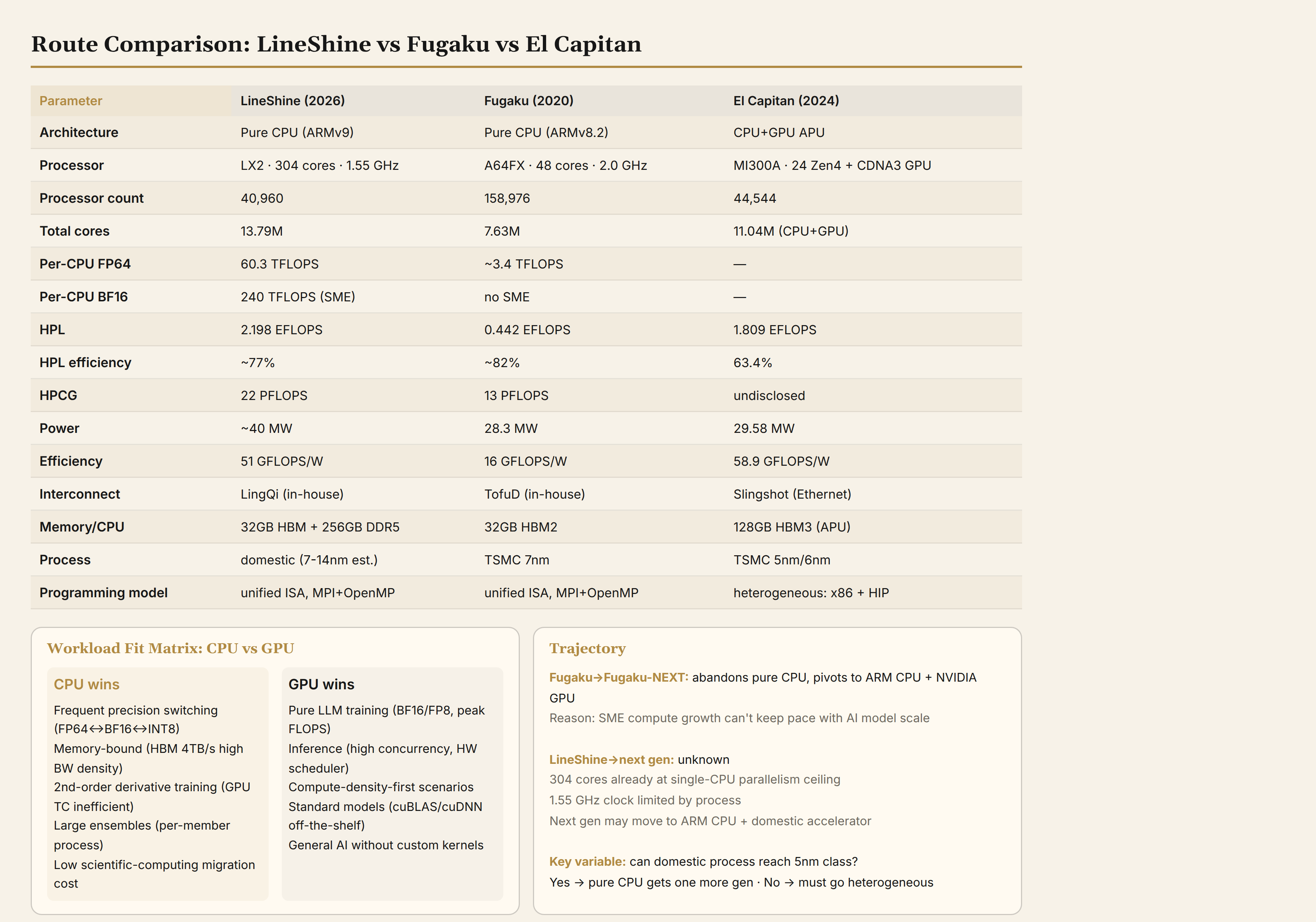
V. Does the Pure CPU Architecture Route Still Have Hope for HPC Clusters?
5.1 The Route's Current Position in Data
The current state of the pure CPU route: LineShine is the most powerful pure-CPU supercomputer ever built, structurally superior to GPU heterogeneous systems in specific domains (scientific computing training, mixed-precision workflows, dense computation). But in mainstream AI training (LLM) and inference, the gap with GPUs is widening, not narrowing.
Comparing LineShine against two reference points:
vs. Fugaku (same route, previous generation):
| Parameter | Fugaku (A64FX, 2020) | LineShine (LX2, 2026) | Change |
|---|---|---|---|
| ISA | ARMv8.2 + SVE | ARMv9 + SVE2 + SME | SME is the watershed |
| Cores/CPU | 48 | 304 | 6.3× |
| FP64/CPU | 3.4 TFLOPS | 60.3 TFLOPS | 18× |
| BF16/CPU | No matrix acceleration | 240 TFLOPS | From zero to exists |
| HPL | 442 PFLOPS | 2,198 PFLOPS | 5× |
| HPCG/HPL | 2.9% | 1.0% | Regressed |
| Efficiency | 16 GFLOPS/W | 51 GFLOPS/W | 3.2× |
| Process | TSMC 7nm | Domestic (estimated 7nm) | From external to self-sufficient |
In six years, the pure CPU route: FP64 up 18×, BF16 from zero to 240 TFLOPS, energy efficiency up 3.2×. The route is still iterating — it has not stagnated.
But HPCG/HPL regressed from 2.9% to 1.0%. More cores, larger shared L2, higher aggregate bandwidth — these design choices optimized for dense computation at the cost of sparse workload efficiency. The route is increasingly specializing toward "dense compute only," with generality narrowing.
vs. El Capitan (heterogeneous route, current benchmark):
| Parameter | LineShine | El Capitan |
|---|---|---|
| Architecture | Pure CPU | CPU+GPU APU (MI300A) |
| HPL | 2.198 EFLOPS | 1.809 EFLOPS |
| HPL efficiency | ~77% | 63.4% |
| Efficiency | 51 GFLOPS/W | 58.9 GFLOPS/W |
| Memory/unit | 32GB HBM + 256GB DDR5 | 128GB HBM3 (APU unified) |
| BF16 compute/CPU | 240 TFLOPS | ~1300 TFLOPS (GPU portion) |
| Programming model | Unified ISA, MPI+OpenMP | x86 + HIP heterogeneous |
HPL efficiency: LineShine 77% vs. El Capitan 63.4% — pure CPU avoids cross-device synchronization overhead, making it naturally more efficient for dense computation.
The BF16 compute density gap is enormous: LX2's 240 TFLOPS vs. MI300A's approximately 1,300 TFLOPS (GPU portion). In the face of AI training's insatiable demand for absolute compute, this 5.4× gap means a GPU cluster can match the same training throughput with far fewer compute units.
The memory capacity gap is equally critical: MI300A's 128 GB HBM3 vs. LX2's 32 GB HBM. El Capitan can hold a 70B LLM's training state in a single APU's HBM; LineShine cannot.
5.2 Why Japan Pivoted to Heterogeneous
Japan's Fugaku-NEXT will adopt a Fujitsu Monaka ARM CPU + NVIDIA GPU heterogeneous architecture. The logic of this decision lies not in technology itself — Fugaku was unequivocally the world's #1 in 2020–2021 — but in workload shifts.
When Fugaku was designed circa 2020, HPC's dominant workloads were scientific simulations (CFD, weather, seismology, materials) — FP64 dense compute, perfectly suited to pure CPU architecture. By 2024–2026, AI training workloads had exploded in both scale and proportion — LLM parameters grew from tens of billions to trillions, and training compute requirements multiplied several-fold each year. CPU SME units cannot scale at this pace:
- Core count is bounded by L2 bandwidth: 38 cores/cluster × 8 = 304, already at the current L2 configuration's limit
- Clock frequency is bounded by process: 1.55 GHz on domestic 7nm-class technology
- Power at 700W/CPU is already near the limit of direct liquid cooling
- Adding more SME pipelines requires more die area, but the reticle limit forces chiplets, which introduce cross-die latency
Every dimension has reached the point of sharply diminishing marginal returns. Next-generation GPUs (NVIDIA Rubin, AMD MI450) will push BF16 into the 3,000–5,000 TFLOPS range. To push LX2's SME to 1,000 TFLOPS BF16 would require quadrupling the SME pipeline count — 4 SME pipelines per core, increasing die area by 40–60%, pushing power beyond 1,000 W/CPU. Under current packaging and cooling technology, this is unrealistic.
Japan's pivot to heterogeneous was not because pure CPU "failed," but because AI workloads' growth curve vastly outpaces the CPU matrix unit's scaling curve. When the gap between these two curves exceeds 10×, the route choice is no longer a matter of preference.
5.3 Quantitative Capability Boundaries of the Pure CPU Route
Drawing from the three cases in Section IV and the architectural analysis above, the pure CPU route's capability boundaries can be quantitatively stated:
Model size ceiling: approximately 6–7B parameters (BF16 + Adam). Determined by 32 GB HBM capacity. This reflects current domestic HBM production constraints. If domestic HBM3 capacity rises to 64–96 GB per stack, the ceiling could reach 15–20B. But mainstream LLMs have already surpassed this scale.
MFU ceiling: approximately 25–30% (BF16). Determined by HBM bandwidth and SDMA scheduling overhead. Breaking through requires larger HBM bandwidth (>8 TB/s) or more aggressive memory management. GPUs achieve approximately 50–55% MFU on equivalent workloads.
FP32 training efficiency advantage zone: second derivatives + irregular compute graphs. Within this zone, CPU utilization is structurally higher than GPU (MatRIS-MoE: 35.5% vs. 25.4%). But this zone represents a small fraction of the overall AI training market — most training is first-order LLM, where GPUs are more efficient.
Mixed-precision workflows: an irreplaceable structural advantage. Numerical+AI hybrid (the CAPES pattern) is simplest to program and most efficient on pure CPU. But this class of workflow is also not mainstream in the overall HPC market.
System scale sweet spot: 20,000–40,000 CPUs. Below this range, compute time is too long; above it, communication overhead begins eroding efficiency. LineShine's 40,960 CPUs is near the upper bound.
Mapping these boundaries visually:
Workload type              Pure CPU route position
──────────────────────────────────────────────────────
uMLIP / scientific training  ██████████ CPU structural advantage
Mixed precision (num+AI)    ██████████ CPU irreplaceable
CFD / weather simulation    ███████░░░ CPU efficient, GPU also viable
Standard BF16 AI training   ███░░░░░░░ GPU 5× compute density advantage
LLM training (>20B)         ░░░░░░░░░░ HBM capacity insufficient
LLM inference               ░░░░░░░░░░ GPU overwhelming advantage
Sparse / graph computing    ░░░░░░░░░░ HPCG = 1%
5.4 How Many Generations Does This Route Have Left?
LineShine's LX2 has hit four physical boundaries of pure CPU architecture: L2 bandwidth (38 cores/cluster limit), power density (700 W/CPU), HBM capacity (32 GB), and clock frequency (1.55 GHz).
The next generation on the same process node has limited room for improvement — core count cannot increase (L2 bandwidth is saturated), clock frequency cannot rise (process unchanged), and power is already at the ceiling. The only path forward is a process node transition.
If domestic process migrates from 7nm to 5nm:
- Core density increases approximately 70–80% (5nm vs. 7nm logic density ratio) → single die could hold ~250 cores (currently ~150 cores/die at 7nm)
- Clock frequency increases 30–50% → 2.0–2.3 GHz
- Same-performance power drops 30% → or same-power performance increases 40–50%
- Room for larger SME units or more cores
- Estimate: a 5nm next-gen LX2 could reach FP64 ~100 TFLOPS, BF16 ~400 TFLOPS, approximately 60 cores/cluster × 8 = 480 cores
If reaching 3nm (likely 3–5 years out):
- Core density doubles → ~500–600 cores/CPU (requires redesigning the L2 hierarchy, likely 12–16 clusters)
- Clock frequency 2.5–3.0 GHz
- FP64 ~200 TFLOPS, BF16 ~800 TFLOPS
- This approaches current H100's BF16 compute, but still falls far short of next-generation GPUs (Rubin expected at 3,000+ TFLOPS BF16)
How many generations does the pure CPU route have left?
At 5nm, the pure CPU route has one more strong iteration — BF16 rising from 240 to ~400 TFLOPS, FP64 from 60 to ~100 TFLOPS, efficiency from 51 to ~70 GFLOPS/W. This generation would maintain structural advantages in scientific computing training and mixed-precision workflows, while narrowing the gap in standard AI training from 5.4× to ~3×.
At 3nm — if domestic 3nm reaches mass production in a reasonable timeframe — the pure CPU route has one final generation. Beyond that, the compute density gap between CPU and GPU will widen again, because GPU specialization extracts more FLOPS per square millimeter of silicon.
Final assessment: the pure CPU route still has hope in HPC clusters, but the window is narrowing. In scientific computing training, mixed-precision workflows, and dense FP64 computation, it remains the optimal choice — not a runner-up, but structurally optimal. In the mainstream AI training and inference market, however, the GPU heterogeneous route's compute density advantage continues to widen.
The most likely evolutionary path after LineShine is not a continuation of pure CPU, but a move toward "ARM CPU + domestic accelerator" heterogeneity — using an LX2 successor for general-purpose and FP64 scientific computing, paired with a domestic AI accelerator (possibly based on the Ascend architecture or an entirely new design) for BF16/FP8 large-scale training. This mirrors Fugaku-NEXT's logic: preserve the ARM CPU's scientific computing advantage and programming simplicity, while introducing a dedicated accelerator to cover the AI training compute gap.
This is not the failure of the pure CPU route. It is the route's natural evolution — from "one architecture for everything" toward a division of labor: "CPU for scientific computing, accelerator for AI training." LineShine has reached the highest point of pure CPU architecture, and also the fork in the road.
Disclaimer: This article is based on publicly available information, drawing from the ISC 2026 TOP500 list, arXiv papers 2604.15821 / 2605.08633 / 2605.24896, Tom's Hardware reporting, official information from the National Supercomputing Center in Shenzhen, and public technical documentation from Fujitsu and AMD. The microarchitecture analysis is based on inference from the ARMv9 architecture specification, Neoverse reference designs, and physical constraints. Content marked as "inferred" or "estimated" represents reasonable deduction rather than confirmed fact. This article does not constitute investment or strategic advice. Data is current as of June 24, 2026. Cover and machine-room photo: Science and Technology Daily (reporter Luo Yunpeng; via Guangming Online, June 24, 2026); photo provided by the National Supercomputing Center in Shenzhen.