On May 25, 2026, Huawei's He Tingbo unveiled "Tau Scaling" at ISCAS 2026, claiming to replace "geometric scaling" with "temporal scaling"—boosting performance through architectural innovation rather than smaller process nodes. Three days earlier, a Peking University team announced a "true 3D" EDA tool prototype. A month before that, SkyWater in the U.S., working with MIT and Stanford, fabricated the world's first carbon nanotube monolithic 3D chip prototype. Meanwhile, TSMC is pushing SoIC interconnect pitch from 6μm toward 4.5μm, and Intel's PowerVia backside power delivery has entered mass production on the 18A process.
The semiconductor industry is simultaneously pursuing 3D stacking. But they are not all doing the same thing.
I. Three Generations of Packaging Technology Evolution
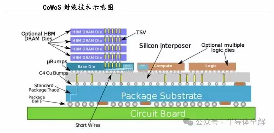
3D integration is not a new concept. Research institutions began experimenting with vertical chip stacking in laboratories as early as the late 1970s. However, it wasn't until around 2010, when TSMC launched CoWoS (Chip-on-Wafer-on-Substrate—arranging multiple independent dies laterally on a silicon interposer and integrating them via high-bandwidth interconnects), Intel introduced EMIB (Embedded Multi-die Interconnect Bridge—using embedded silicon bridges instead of large-area silicon interposers for high-speed die-to-die connections), and Samsung debuted I-Cube, that advanced packaging truly entered large-scale commercial deployment.
By the industry's conventional classification, 3D integration has evolved through three generations:
First Generation: Package-Level 3D Stacking (Parallel 3D Integration). Represented by HBM (High Bandwidth Memory—high-bandwidth memory that vertically stacks multiple DRAM dies through TSVs) and AMD's 3D V-Cache. The essence is connecting multiple independent dies at the packaging stage using TSVs (Through-Silicon Vias—vertical holes drilled through silicon and filled with metal conductors to enable electrical connections between layers) and microbumps. This technology is mature and already in mass production.
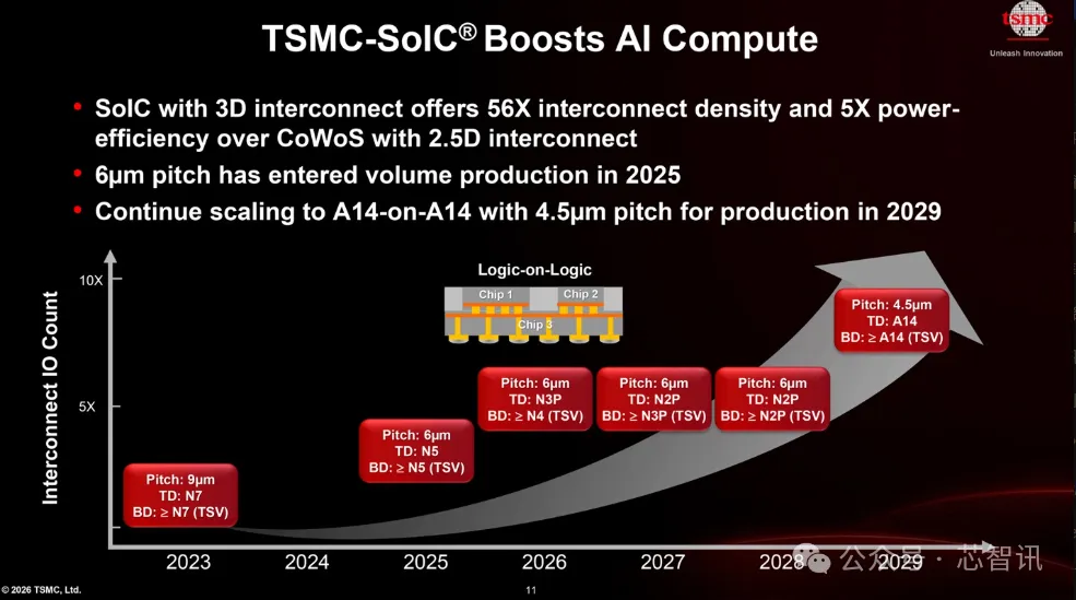
Second Generation: Wafer-Level 3D Stacking (Advanced Chiplet Integration). Represented by TSMC's CoWoS and SoIC (System-on-Integrated-Chips—a 3D packaging platform that achieves high-density inter-wafer interconnects through hybrid bonding). In 2026, TSMC reduced the SoIC interconnect pitch to 6μm, targeting 4.5μm by 2029. More critically, second-generation technology is transitioning from face-to-back (where signals must traverse TSVs through the bottom die) to face-to-face (where the active metal layers of two dies align directly, connected through hybrid copper bonding). Broadcom's measured data shows face-to-face stacking achieving a signal density of 14,000 signals per square millimeter—nearly 10× the 1,500 of face-to-back.
Third Generation: Monolithic 3D Integration (M3D). This is "true 3D"—sequentially fabricating multiple layers of active transistors on the same wafer, achieving inter-layer communication through lithography-grade nanometer precision, rather than bonding separately manufactured dies together. In December 2025, SkyWater, in collaboration with MIT and Stanford, fabricated the world's first carbon nanotube monolithic 3D chip prototype, achieving 4× the performance of comparable 2D chips on a 90nm process.
The fundamental distinction between the three generations: the first two "stack completed buildings together"; the third "builds floors sequentially on the same foundation."
II. Where Chip Manufacturing Stands Today
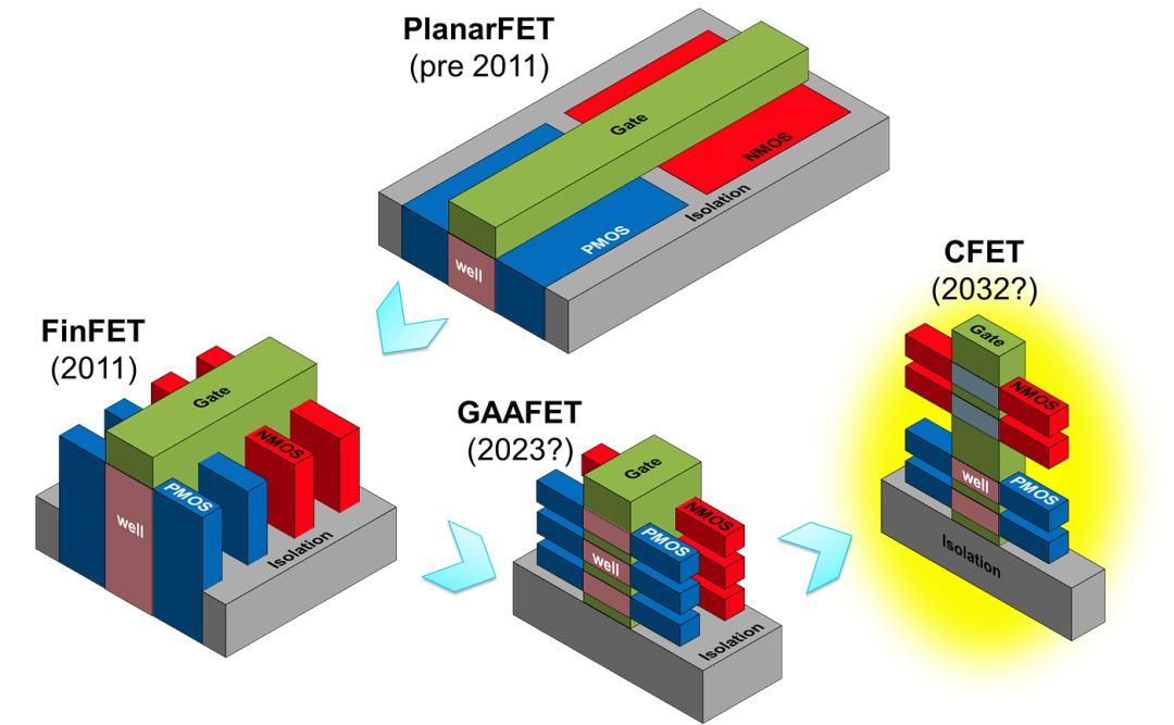
Transistor Architecture: FinFET → GAA → CFET
TSMC's N2 (2nm) and Intel's 18A are the most advanced mass-production processes today. Both have transitioned from FinFET (Fin Field-Effect Transistor—controlling current through upright "fin" structures on three sides) to GAA (Gate-All-Around—the gate wraps around the nanosheet channel on all four sides, providing more precise electrostatic control).
TSMC's N2 delivers a 10-15% speed improvement at the same power, or 25-30% power reduction at the same speed. Samsung adopted GAA first at 3nm (its MBCFET path), but yield issues have diminished the advantage.
After GAA comes CFET (Complementary FET), which vertically stacks N-type and P-type transistors, theoretically doubling transistor density again. imec's roadmap shows CFET being introduced at the A14/A10 node, paired with High-NA EUV (High Numerical Aperture Extreme Ultraviolet Lithography—NA rising from 0.33 to 0.55, resolution improving from 13nm to 8nm).
Backside Power Delivery (BSPDN): Rewiring the Layout
Intel pioneered PowerVia backside power delivery in mass production on its 18A process—moving the power delivery network from the wafer's front side to the back, freeing the front entirely for signal routing. Measured data shows that GAA + backside power delivery can boost operating frequency by 25% at the same voltage, or reduce power consumption by 36%.
TSMC's A16 process will also introduce "Super Power Rail" backside power delivery. Nomura reports note that backside power delivery requires bonding two wafers together, nearly doubling wafer consumption, with CMP (Chemical Mechanical Planarization) steps increasing by 20-30%.
Process Roadmaps: The Three Giants Diverge
| Vendor | Current Node | High-NA EUV Stance | Backside Power |
|---|---|---|---|
| TSMC | N2 (2025 mass production) | "Too expensive, not buying"; not needed before A13 | A16 introduction |
| Intel | 18A (2025 mass production) | Most aggressive; two machines installed | 18A in production |
| Samsung | SF2 (2026 mass production) | Originally 2027, delayed to 2029 | SF2Z introduced |
TSMC's logic is pragmatic: one High-NA EUV costs approximately $400 million, double that of existing EUV. Replacing the 100+ installed EUV machines would require tens of billions of dollars. They plan to bridge to A13 using mature EUV multi-patterning, and consider High-NA when the cost-performance ratio becomes favorable.
III. Huawei's Tau Scaling: Trading Architecture for Time
Core Philosophy
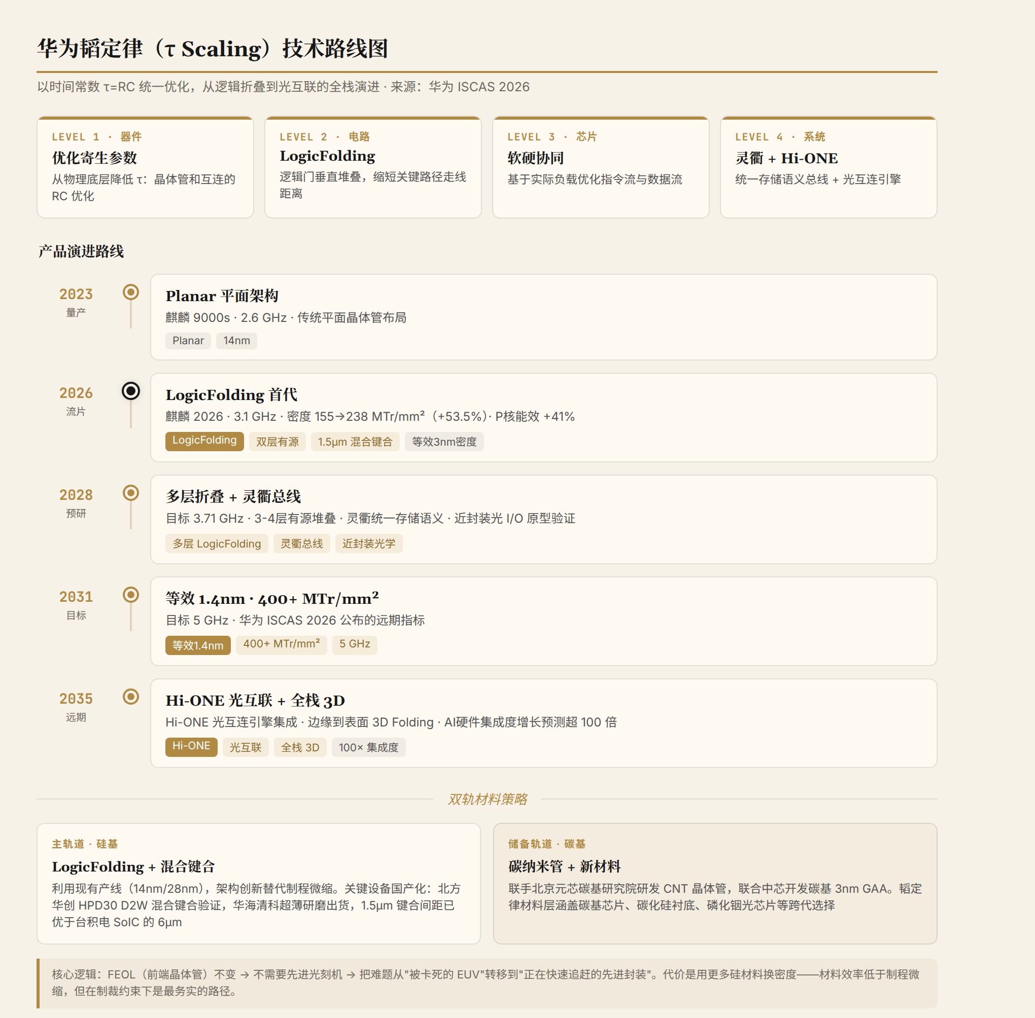
On May 25, 2026, Huawei Semiconductor Division President He Tingbo formally presented "Tau (τ) Scaling" at ISCAS 2026: replacing "geometric scaling" with "temporal scaling," continuously improving system-equivalent performance by compressing signal propagation delay across all hierarchy levels (τ = RC, the time constant equals resistance multiplied by capacitance).
Tau Scaling spans four levels:
- Device Level: Optimizing parasitic parameters of transistors and interconnects, reducing τ from the physical foundation
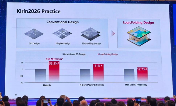
- Circuit Level: LogicFolding—vertically stacking flat logic gate circuits, shortening critical path wiring
- Chip Level: Hardware-software co-design, optimizing instruction and data flows based on actual workloads
- System Level: Lingqu Bus + Hi-ONE Optical Interconnect Engine, unifying system interconnect protocols
LogicFolding vs. Traditional 3D Stacking: Not the Same Thing
This is where confusion most often arises. Many assume "LogicFolding is just 3D packaging with a different name." In reality, they operate at fundamentally different levels of technology abstraction:
| Dimension | Traditional 3D Stacking (CoWoS/SoIC/Foveros) | Huawei LogicFolding |
|---|---|---|
| Target | Between multiple independent dies | Logic layers within a single die |
| Problem Solved | "How close can different chips get" | "How far does the signal itself need to travel" |
| Technology Level | Manufacturing/packaging process | Chip design/circuit topology |
| Interconnect Pitch | 6μm (SoIC), tens of μm (TSV) | ~1.5μm (inter-layer TSV) |
| Prerequisite | Requires advanced process support | Does not depend on advanced processes |
A more direct analogy: 3D stacking is like using a crane to place two already-built buildings on top of each other and installing elevators between floors. LogicFolding is like redesigning the floor plans of a single building from the blueprint stage, so rooms that previously required an elevator to reach become directly connected between adjacent floors.
Key Data: Kirin 2026 (the first LogicFolding commercial chip) increased transistor density from 155 MTr/mm² to 238 MTr/mm² (+53.5%) without relying on more advanced lithography equipment, with P-core energy efficiency improving 41% and clock speed reaching 3.1GHz. This density approaches TSMC's initial 3nm (~280 MTr/mm²), equivalent to jumping two process generations on existing manufacturing.
The Cost of Density Gains: Footprint Density vs. Silicon Material Efficiency
There's an important nuance here. The 238 MTr/mm² figure is "footprint density"—how many transistors exist per square millimeter of chip package area. From the user's perspective, the chip in their phone is indeed smaller and more powerful.
But LogicFolding achieves this by vertically stacking two active layers. Theoretically, two layers should deliver approximately 100% density doubling. In practice, only 53.5% was achieved—roughly half the theoretical gain was consumed. Reasons include: inter-layer TSVs occupying area (the 1.5μm pitch array itself takes up silicon real estate), bonding interface alignment marks and interface materials, thermal channels and thermal vias crowding out transistor space, and TSVs being moved from top-level metal down to M6, which freed routing resources but M6 itself serves other purposes.
A more direct comparison with TSMC's 3nm: TSMC achieved ~280 MTr/mm² using single-layer silicon with process scaling. Huawei achieved 238 MTr/mm² using approximately twice the silicon material (two active layers). In terms of transistor output efficiency per unit of silicon material, LogicFolding's efficiency is actually lower than advanced process scaling.
This doesn't mean the Tau Scaling path lacks value—quite the opposite. Its value lies in providing a viable performance leap path for companies that cannot access advanced processes. It's simply important to understand that this is a "materials-for-density" route, fundamentally different from Moore's Law's "precision-for-density" in terms of resource consumption.
Stack Layers: Where Is Each Route's Ceiling?
Stack layer count is a critical parameter for understanding each technology path's ceiling:
| Technology Route | Current Stack Layers | Near-Term Target | Core Limitation |
|---|---|---|---|
| HBM (Memory Stacking) | 12 layers in production (HBM3E) | 16-20 layers (HBM4) | Thermal resistance accumulation: bottom die heat must traverse all upper layers to reach the heatsink. 4-layer HBM2 stacking can have a 24°C internal temperature differential |
| TSMC SoIC (die-to-die) | 2 layers (face-to-face) | More heterogeneous combinations | Each additional die requires another wafer bonding step; yield loss compounds |
| Intel Foveros | 2-3 layers | Foveros Direct 3+ | Same as SoIC, but higher hybrid bonding precision (12.5μm pitch) |
| Huawei LogicFolding | 2 active layers (Kirin 2026) | 3-4 active layers (paper roadmap) | Thermal density catastrophe: vertically stacked active logic layers generate far more heat than memory stacking; power density increases geometrically |
| Carbon Nanotube M3D | 4 layers (SkyWater prototype) | Theoretically unlimited | Low-temperature process (<200°C) solves thermal budget constraints; the only route not thermally limited |
| 3D NAND (Reference) | 300+ layers | 400+ layers | Memory cells generate negligible heat; logic layer stacking is not directly comparable |
Key Distinction: Memory Stacking vs. Logic Layer Stacking. HBM can reach 12-16 layers and 3D NAND exceeds 300 layers because memory cells generate minimal heat (~5-10W per DRAM layer, NAND layers generate almost no heat). Logic layers have 10-100× the power density per square millimeter. Huawei's two active logic layers delivered 53.5% density improvement but already reached the thermal limits of phone form factors; data centers with more generous cooling have more headroom for stacking.
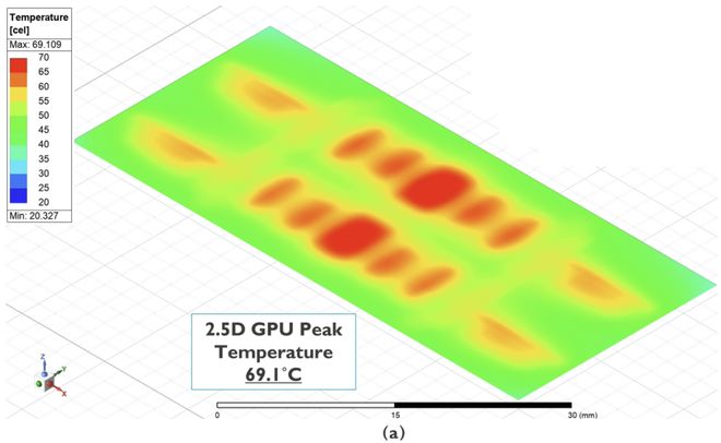
imec's research published at IEDM 2025 visually demonstrates this ceiling: placing four 12-layer HBM stacks directly on top of a 400W GPU caused GPU temperature to surge from 70°C to 142°C—far exceeding the 80°C operational limit for chips. Even after a series of extreme optimizations (removing HBM base dies, merging stacks, reducing frequency by 50%, implementing dual-sided liquid cooling), the temperature could only be brought down to approximately 70°C. The trade-off was sacrificing half the raw compute power for a 4× memory bandwidth increase, yielding a net 22-46% performance improvement. This demonstrates that HBM-on-GPU 3D stacking is "barely feasible" in engineering terms, but at enormous cost.
The Costs Are Real
Tau Scaling's "grand shift" moves the EUV lithography challenge to the 3D ecosystem, but the difficulty hasn't decreased:
- Thermal Balance Catastrophe. Vertical stacking causes power density per unit area to increase geometrically. He Tingbo herself acknowledged that "the thermal problem spans 12 orders of magnitude."
- Process and Yield Black Holes. Heterogeneous wafer bonding requires copper pad surface roughness <0.5nm, bonding alignment accuracy <50nm, and ISO Class 3 cleanrooms. A 1μm particle can cause a bonding void 10mm in diameter.
- EDA Tool Chain Gap. Mainstream EDA remains in the 2D planar era. 3D design requires holistically considering timing, thermal, power integrity, signal integrity, and mechanical stress in three-dimensional space. The PKU team's "true 3D" EDA prototype shows this problem is recognized, but industrialization remains distant.
LogicFolding's Process Flow: What's Added Beyond Traditional 2D
LogicFolding is significantly more complex than traditional 2D chip manufacturing in process terms, but the complexity concentrates in the middle-to-back-end (MEOL/BEOL/packaging). Front-end transistor fabrication (FEOL) remains essentially unchanged—this is the key enabler for Tau Scaling.
Traditional 2D chip flow: FEOL (transistor fabrication) → MEOL (local interconnects) → BEOL (metal routing) → dicing → packaging → testing. LogicFolding adds multiple high-difficulty steps on top of this flow:
Wafer Ultra-Thinning (New). Two active layers each need to be thinned to 20-50μm, with thickness control accuracy of ±0.2μm (versus traditional ±2μm). Thinned wafers are extremely fragile and must be temporarily bonded to carrier wafers before further processing.
TSV Fabrication (Significantly Increased). Traditional chips may not need TSVs at all; LogicFolding creates TSVs at the M6 metal layer, with aspect ratios increasing from 5:1 to 20:1, via diameters of 1-5μm, and sidewall roughness <1nm. A single Ascend 950 chip requires 100,000+ TSV vias.
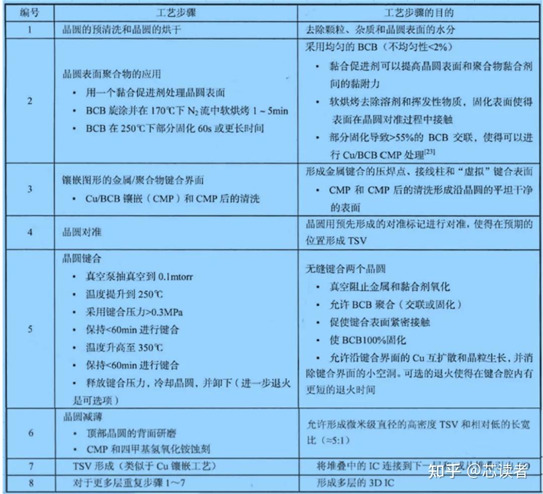
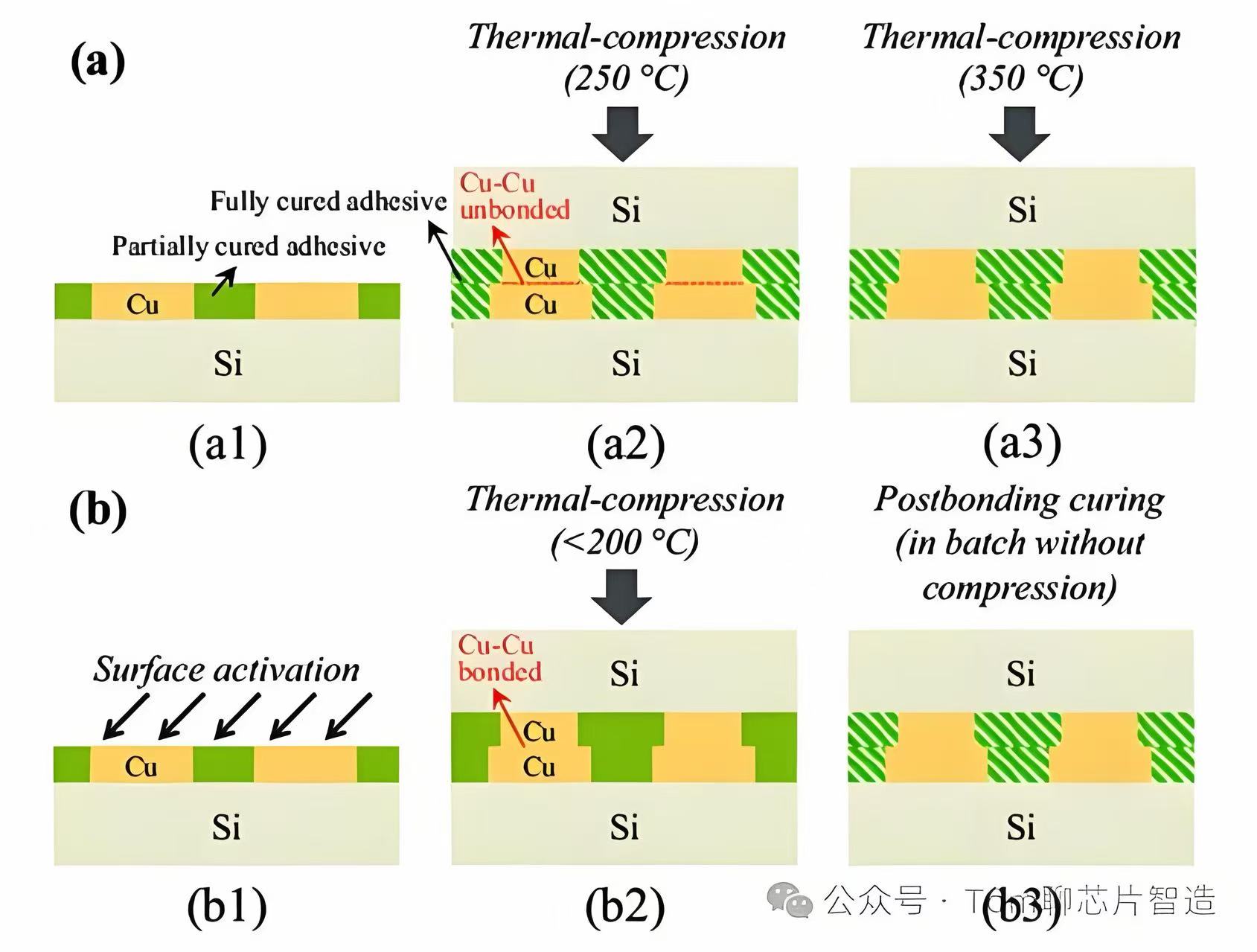
Low-Temperature Hybrid Bonding (New, Most Critical). The two active layers are connected through copper-to-copper direct bonding, with alignment accuracy ≤0.3μm (versus 1μm in traditional packaging), bonding temperature <200°C (to protect already-fabricated transistors in the bottom layer), and copper pad surface roughness <0.5nm. This is the highest-precision step in the entire process.
Temporary Bonding/Debonding (New). Each stacked layer consumes one temporary bonding/debonding cycle—bonding to a carrier before thinning, then separating after processing (temperature <150°C, warpage <50μm).
CMP Steps Doubled. Hybrid bonding demands extremely high surface flatness; CMP process steps increase by 20-30% compared to traditional.
Testing Goes from 2 to 6+ Cycles. Test before each layer stacking, test after stacking, test after bonding... the packaging and testing workload multiplies.
Wafer Consumption Nearly Doubles. Two active layers means each chip consumes approximately 2 wafers of material.
| Step | Traditional 2D | LogicFolding | Change Magnitude |
|---|---|---|---|
| FEOL (Transistors) | Normal | Unchanged | 0 |
| MEOL (Local Interconnects) | Normal | Added TSVs | +3-5 steps |
| BEOL (Metal Routing) | Normal | TSVs moved to M6 | Routing strategy changed |
| Wafer Thinning | Not needed | 20-50μm, ±0.2μm | New |
| Hybrid Bonding | Not needed | ≤0.3μm accuracy, <200°C | New, Biggest Bottleneck |
| Temporary Bonding/Debonding | Not needed | Once per layer | New |
| CMP | Normal | +20-30% | Significant increase |
| Testing | 2 times | 6+ times | 3×+ |
| Wafer Consumption | 1 wafer/chip | ~2 wafers/chip | Nearly doubled |
Core conclusion: Unchanged FEOL means no advanced lithography equipment is needed. SMIC's existing production lines (14nm/28nm) don't require major modifications. All new complexity is in the middle-to-back-end and packaging—precisely where domestic substitution is progressing fastest. This explains why Tau Scaling is viable for Huawei: it shifts the challenge from "EUV, where they're blocked" to "advanced packaging, where they're rapidly catching up."
Equipment Bottlenecks: Which Require New Designs, Which Can Be Upgraded
Equipment needed for LogicFolding, ranked by bottleneck severity:
Hybrid Bonding Equipment — Entirely New Design, the Only True Chokepoint. Cannot be converted from existing equipment; must be purpose-built. The Netherlands' BESI holds approximately 67% global market share; the top five hold 86%. Single unit price exceeds ¥100 million; overseas delivery lead time exceeds 52 weeks. Domestic progress: NAURA exhibited the Qomola HPD30 at SEMICON China 2026, completing D2W hybrid bonding client-side process verification (first in China); Piotech has W2W mass-production models. Huawei achieved a bonding pitch of approximately 1.5μm, already superior to TSMC's current SoIC mass production at ~6μm.
Wafer Thinning Equipment — Major Upgrade, Not from Scratch. Traditional thinning to ~200μm is sufficient; LogicFolding requires 20-50μm. Existing equipment's spindle precision and cooling systems can't reach this level, so it can't be simply modified. But thinning equipment isn't starting from zero like hybrid bonding. HWATSING introduced its first ultra-thin grinding equipment in April 2026; Xinyuantang and Yitang Semiconductor's 12-inch double-sided thinning machines have been validated at JCET with 99.2% yield.
CMP — Existing Equipment with Upgraded Process Parameters and Consumables. CMP isn't new equipment—fabs already have extensive installed bases. LogicFolding raises surface roughness requirements from 1-2nm to <0.5nm, primarily achieved through new slurry formulations and polishing pads. HWATSING's CMP equipment has large-scale installed bases domestically; this segment has relatively high localization rates.
TSV Etching — Existing Equipment with Upgraded Parameters. Uses ICP etchers already present in fabs; requires increasing aspect ratios from 5:1 to 20:1. AMEC and NAURA already have high-aspect-ratio etching equipment. NAURA's NMC612H has pushed aspect ratios to hundreds-to-one.
Temporary Bonding/Debonding — Relatively New but Simple in Principle. This process step is borrowed from CIS and 3D NAND fields. HWATSING and Xinqi Micro already have products.
| Equipment Category | New vs. Upgradeable | Domestic Progress | Bottleneck Level |
|---|---|---|---|
| Hybrid Bonding | Entirely New | NAURA/Piotech verified | Critical |
| Wafer Thinning | Major Upgrade | HWATSING shipped | High |
| CMP | Upgrade Process + Consumables | HWATSING mature | Medium |
| TSV Etching | Parameter Upgrade | AMEC/NAURA available | Medium |
| Temporary Bonding/Debonding | New but Simple | HWATSING/Xinqi available | Low |
Signal Worth Tracking: Huawei achieved a hybrid bonding pitch of 1.5μm, outperforming TSMC SoIC's 6μm—either through higher equipment precision or a different process route (W2W vs D2W, or different bonding schemes). If domestic hybrid bonding equipment truly supports 1.5μm pitch mass production, it's significantly ahead of external perceptions.
Huawei's Dual-Track Strategy
It's worth noting that Huawei is not entirely dismissive of the carbon-based route. Tau Scaling encompasses cross-generational material choices at the material level, including carbon-based chips, silicon carbide substrates, and indium phosphide photonic chips. Huawei has partnered with Beijing Yuanxin Carbon-Based Integrated Circuit Research Institute to develop carbon nanotube transistors and is collaborating with SMIC to develop carbon-based 3nm GAA chips. Silicon-based as primary, carbon-based as reserve.
IV. Comparing the Two Routes
U.S.: Carbon Nanotube M3D, Disruption from the Material Foundation
DARPA's 3DSoC program ($61 million single-project funding) has a clear goal: use mature 90nm processes to achieve 50× the performance-per-watt of 7nm. MIT's Shulaker team vertically stacks carbon nanotube transistors (CNFETs) with RRAM, forming a logic-memory-interleaved 3D architecture.
Carbon nanotube advantages:
- Interconnect density 10,000× higher than TSV (MIV diameter ~100nm vs. micrometer-scale TSV)
- Energy-delay product over 10× superior to silicon CMOS
- Low-temperature process (<200°C), solving silicon M3D's thermal budget challenge
- Thermal conductivity 1000-6600 W/m·K, far exceeding copper's ~400 W/m·K
But mass production remains 5-10 years away. Core bottlenecks: precise alignment and high-density arrangement of carbon nanotubes, large-area wafer uniformity, and translating from prototype to foundry.
China: Tau Scaling + Silicon-Based 3D, Trading Architecture for Time
Huawei's route is more pragmatic: on the existing silicon-based industrial foundation, achieving performance leaps through design-level innovation (LogicFolding + optical interconnects + system-level co-optimization). The 381-chip production validation is the core argument—this is not a laboratory concept but an engineering route that has successfully run through industrial mass production.
The strategic divergence of the two routes: the U.S. is mounting a strategic offensive from the material foundation, attempting to redefine the bedrock of chip manufacturing. Huawei is executing a realistic breakout under advanced process restrictions, using mature capacity and architectural innovation to buy time and space.
V. Key Judgments
Highest-Confidence Trends
Advanced packaging has upgraded from "back-end supporting role" to "performance determinant." This isn't Huawei's judgment alone—it's an industry-wide consensus. TSMC's CoWoS capacity has tripled in three years and still can't meet demand; SoIC is pushing from 6μm toward 4.5μm; Intel's EMIB is being adopted by customers like SK Hynix—the strategic importance of the packaging stage is rising rapidly.
Backside power delivery will accelerate into mass production starting 2027. Intel's 18A has already mass-produced PowerVia; TSMC's A16 and Samsung's SF2Z will follow. Nomura projects backside power delivery will become standard for advanced chips by 2030.
Medium-Confidence Judgments
Huawei's Tau Scaling will deliver far more value in AI data centers than in consumer electronics. AI chips have large die areas, dense inter-chip communication, ample cooling space, and high cost tolerance—these are all ideal conditions for LogicFolding and 3D stacking. Huawei projects AI hardware integration density will grow 100× or more by 2035.
"True 3D" EDA is the next bottleneck. The PKU team's "true 3D" EDA prototype shows the industry recognizes this problem, but moving from prototype to production-grade tools requires 3-5 years. Whoever solves the 3D design tool chain first gains the initiative in 3D chip competition.
Variables Requiring Ongoing Tracking
- Kirin 2026's real-world performance. The first LogicFolding chip launches in fall 2026—transistor density, power consumption, thermal performance, and yield are the key metrics that will validate Tau Scaling.
- Carbon nanotube M3D industrialization pace. The SkyWater prototype is a milestone, but going from prototype to mass production typically takes 5-10 years.
- High-NA EUV cost inflection point. If High-NA EUV proves insufficiently cost-effective and pitch scaling ceases to be the key issue, the entire industry will focus more on 3D structures and packaging innovation—which benefits the Tau Scaling route.
- Hybrid bonding yield ramp. TSMC SoIC's mass-production yield transitioning from face-to-back to face-to-face directly determines the pace of 3D packaging adoption.
Data Summary
| Metric | Data | Source |
|---|---|---|
| TSMC SoIC interconnect pitch (2026) | 6μm | TSMC 2026 North America Technology Forum |
| TSMC SoIC interconnect pitch (2029 target) | 4.5μm | Same as above |
| Face-to-face vs. face-to-back signal density | 14,000 vs. 1,500 /mm² | Broadcom measured |
| Kirin 2026 transistor density | 238 MTr/mm² (+53.5%) | Huawei ISCAS 2026 |
| Kirin 2026 P-core energy efficiency improvement | +41% | Same as above |
| Kirin 2026 clock speed | 3.1GHz (+12.7%) | Same as above |
| Intel 18A GAA + backside power performance gain | +25% frequency or -36% power | VLSI 2025 measured |
| TSMC N2 vs. 3nm power improvement | -25-30% (same frequency) | TSMC official |
| SkyWater CNT M3D performance | 4× that of 2D chip (90nm process) | IEDM 2025 |
| SkyWater CNT M3D stack layers | 4 layers (Si CMOS → RRAM → CNFET logic → CNFET sensor) | IEDM 2025 |
| HBM stack layers (current production) | 12 layers (HBM3E) | SK Hynix |
| HBM stack layers (next target) | 16-20 layers (HBM4) | JEDEC roadmap |
| 3D NAND stack layers (current production) | 300+ layers | Samsung/SK Hynix |
| Huawei LogicFolding current layers | 2 active layers (Kirin 2026) | Huawei ISCAS 2026 |
| Huawei LogicFolding evolution target | 3-4 active layers (10-year plan) | He Tingbo paper |
| imec HBM-on-GPU 3D stacking temperature | 142°C (baseline) → ~70°C (after extreme optimization) | IEDM 2025 |
| Huawei Tau Scaling target (2031) | Equivalent 1.4nm, 400+ MTr/mm², 5GHz clock | Huawei ISCAS 2026 |
| 3D IC market size (2032 forecast) | ~¥845.5 billion (CAGR 12%) | Hengzhou Chengshi |
| High-NA EUV unit price | ~$400 million/unit | ASML |
Disclaimer: This article is based on cross-validated information from Huawei's ISCAS 2026 public presentation, TSMC's 2026 North America Technology Forum, IEDM 2025 papers, Nomura Securities and Goldman Sachs research reports, SemiAnalysis, and other sources. It does not constitute investment advice. Data in this article is current as of May 27, 2026.