On May 25, 2026, He Tingbo presented the τ (Tao) scaling conceptual framework at ISCAS 2026. Thirty-nine days later, the V2 paper appeared on ChinaXiv — accepted by Science China, 23 pages, 32 references, two production-scale validation cases. If V1 was a theoretical manifesto for "looking at semiconductor evolution from a different dimension," V2 answers the harder question: does this path actually work in engineering? How far can it go?
1. What V2 Adds
V1's central claim — replacing "geometric scaling" with "temporal scaling" — is not complicated. The hard part is proving it is more than a change in narrative. V2's additions are almost entirely at the "evidence" level:
Mobile validation: Kirin 2026's LogicFolding measured data expands from a handful of numbers in the ISCAS talk to a complete chip-level comparison table covering power, area, frequency, SRAM, clock tree metrics, and a CPU frequency roadmap from 2023 to 2029.
AI systems validation: This was entirely absent from V1. V2 publicly reveals, for the first time, Huawei's "three-layer τ reduction architecture" for AI systems — Unified Bus (Lingqu), Hi-ONE near-packaged optical engine, and 3D Folding — placed within a single theoretical framework and connected by an N²-vs-N geometric argument.
Methodological upgrade: Section 8 states — "τ scaling is the first scaling principle since Dennard to give the entire stack a shared optimization target." This sentence does not appear in the V1 talk. Its significance is not academic positioning but a signal to the industry chain: for four decades, process engineers and system architects optimized their own metrics (frequency, bandwidth, latency, area) independently. τ scaling gives them a common yardstick. In 1974, Dennard scaling established the principle that "proportional voltage and dimension scaling maintains constant electric field," giving device physicists and circuit designers a shared language. For fifty years since, no one has offered a unified ruler spanning device to system. τ scaling attempts to fill that gap.
2. Kirin 2026: LogicFolding's Complete Scorecard
Core Comparison
V1 offered a few headline numbers. V2 lays out the full table:
| Metric | Kirin 9030 Pro (planar) | Kirin 2026 (LogicFolding) | Change |
|---|---|---|---|
| Transistor density | 155 MTr/mm² | 238 MTr/mm² | +53.5% (paper states 55%) |
| Iso-performance power¹ | 1.0 | 0.59 | -41% |
| Die area | 1.0 | 0.625 | -37.5% |
| SoC P-core frequency | 2.75 GHz | 3.1 GHz | +13% |
| SRAM frequency | baseline | +40% or more | — |
| High-speed global NoC datapath area | baseline | -55% | — |
| Clock buffer count | baseline | -50% | — |
| Clock skew | baseline | -25% | — |
| Wire length (representative core) | baseline | -30% | — |
¹ Iso-performance condition: Kirin 9030 Pro runs at 1.1V / 2.75 GHz; Kirin 2026 at 0.9V / 2.5 GHz delivers equivalent performance with measured power at 0.59×. 3.1 GHz is Kirin 2026's maximum frequency, not under this iso-performance condition.
These numbers collectively indicate: at the same process node, purely through three-dimensional reorganization of circuit topology, the density leap that would previously have required roughly three years of geometric scaling has been achieved.
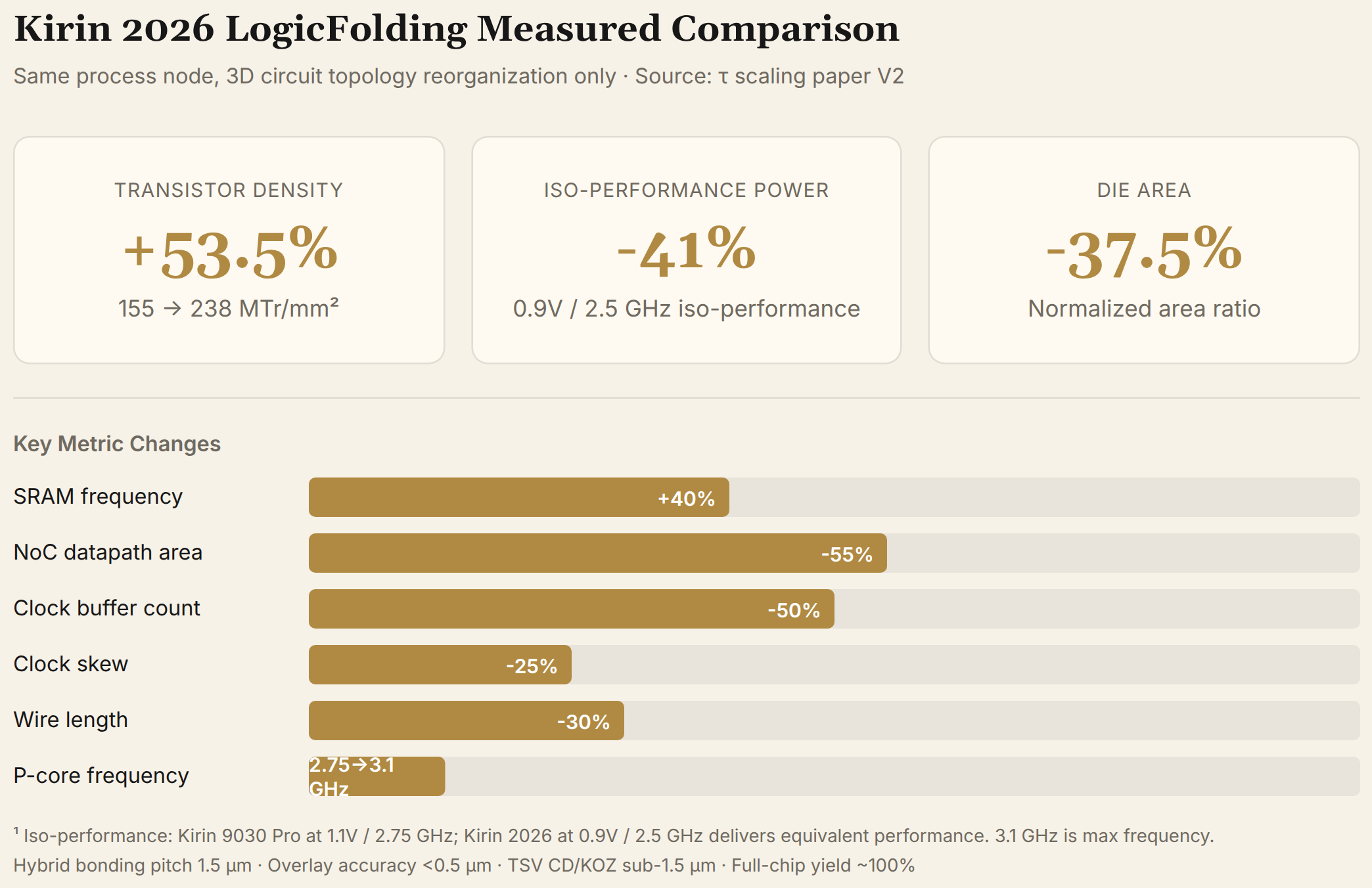
The paper also discloses two easily overlooked but engineering-significant measured results: the high-speed global Network-on-Chip datapath, constructed using both upper and lower active layers, achieved a 55% area reduction while simultaneously improving power delivery stability; and a post-silicon clock skew adjustment scheme independently contributed >5% SoC performance. The former shows LogicFolding is not just "folding logic" — it provides new design freedom for on-chip interconnect topology. The latter suggests the traditional "sign-off is final" boundary is being blurred at the physical implementation level.
Key Process Parameters
The paper discloses LogicFolding's core process metrics:
- Hybrid bonding pitch: 1.5 μm (2026 production version)
- Target gear ratio (pitch ratio): ≈1
- Overlay accuracy: <0.5 μm
- TSV CD/KOZ: sub-1.5 μm, pitch sub-6 μm
- TSV defect rate: <100 ppm, repair rate 99.9%
- Full-chip yield: ~100% (with intelligent redundancy)
Gear Ratio: From Discrete to Continuous Design Paradigm
One of the most theoretically profound yet easily overlooked concepts in the paper is gear ratio.
Gear ratio is defined as the ratio of hybrid bonding pitch to top-level metal routing pitch. When bonding pitch is much larger than metal pitch (gear ratio >> 1), designers can only perform coarse-grained allocation at the functional block level — assigning entire modules to upper or lower layers, because inter-layer interconnects are too sparse to support finer granularity. This is a discrete optimization problem — computationally tractable but far from globally optimal.
When bonding pitch shrinks to approach metal pitch (gear ratio → 1), the two active layers become, from the circuit designer's perspective, "a continuous fabric" — logic cells can be distributed across wafer boundaries as if on the same metal layer. The design space shifts from discrete to continuous, opening the door to global co-optimization.
Kirin 2026's gear ratio is approximately 2 (1.5 μm bonding / ~720 nm top metal), sufficient to support critical-path-level folding. The paper notes that future TSV penetration from top-level metal to M6 will release over 30% of upper-layer routing resources, pushing gear ratio closer to 1. This is not merely a process improvement — it changes the mathematical nature of chip design.
The paper also notes that Sequential 3D integration (S3D) — building transistor layers sequentially on the same wafer — could theoretically provide device-level or standard-cell-level granularity, but currently faces severe manufacturing bottlenecks, particularly performance degradation of lower-layer devices under thermal budget constraints. LogicFolding chooses wafer-to-wafer hybrid bonding as a commercially viable middle ground, balancing granularity and manufacturability.
The 1.5 μm bonding pitch is already in production (TSMC SoIC currently produces at approximately 6 μm, targeting 4.5 μm by 2029). This disclosure corroborates a previously external inference: domestic hybrid bonding equipment may be more advanced than publicly perceived.
Kirin CPU P-Core Frequency Roadmap
Paper Table 2 provides a complete roadmap from 2023 to 2029:
| Year | Chip | Architecture | P-core frequency | Status |
|---|---|---|---|---|
| 2023 | Kirin 9000s | Planar | 2.6 GHz | Mass production |
| 2024 | Kirin 9020 | Planar | 2.65 GHz | Mass production |
| 2025 | Kirin 9030 Pro | Planar | 2.75 GHz | Mass production |
| 2026 | Kirin 2026 | LogicFolding | 3.1 GHz | Silicon (taped out) |
| 2027 | Kirin 2027 | LogicFolding | 3.39 GHz | Silicon |
| 2028 | Kirin 2028 | LogicFolding | 3.71 GHz | Pre-silicon |
| 2029 | Kirin 2029 | LogicFolding | 4 GHz | Pre-silicon |
From 2023 to 2025, three years of planar architecture yielded only 0.15 GHz improvement. After switching to LogicFolding, 2026 alone gained 0.35 GHz, with a sustained ~0.3 GHz annual improvement slope thereafter. The paper projects transistor density reaching 400+ MTr/mm² by 2035.
The paper emphasizes that the 2026 production version is a "conservative implementation" — LogicFolding is selectively applied to critical paths, with 1.5 μm bonding pitch and TSVs penetrating only one layer below top metal. Future evolution toward three and four active layers, combined with lower-temperature bonding and TSV penetration to M6, leaves substantial design space to be unlocked.
3. AI Data Centers: Three-Layer τ Reduction Architecture
Section 5 is V2's most significant addition. The paper extends τ scaling from mobile chips to AI data centers — not as a simple scenario extension, but by reinterpreting Huawei's existing Lingqu bus, Hi-ONE optical interconnect, and 3D stacking technologies within the unified τ scaling framework.
The paper provides two supporting facts: in AI systems, over 80% of energy consumption goes to data movement and over 70% of system cost is allocated to data storage. These figures mean that reducing the time data spends in transit is at least as important as reducing computation time.
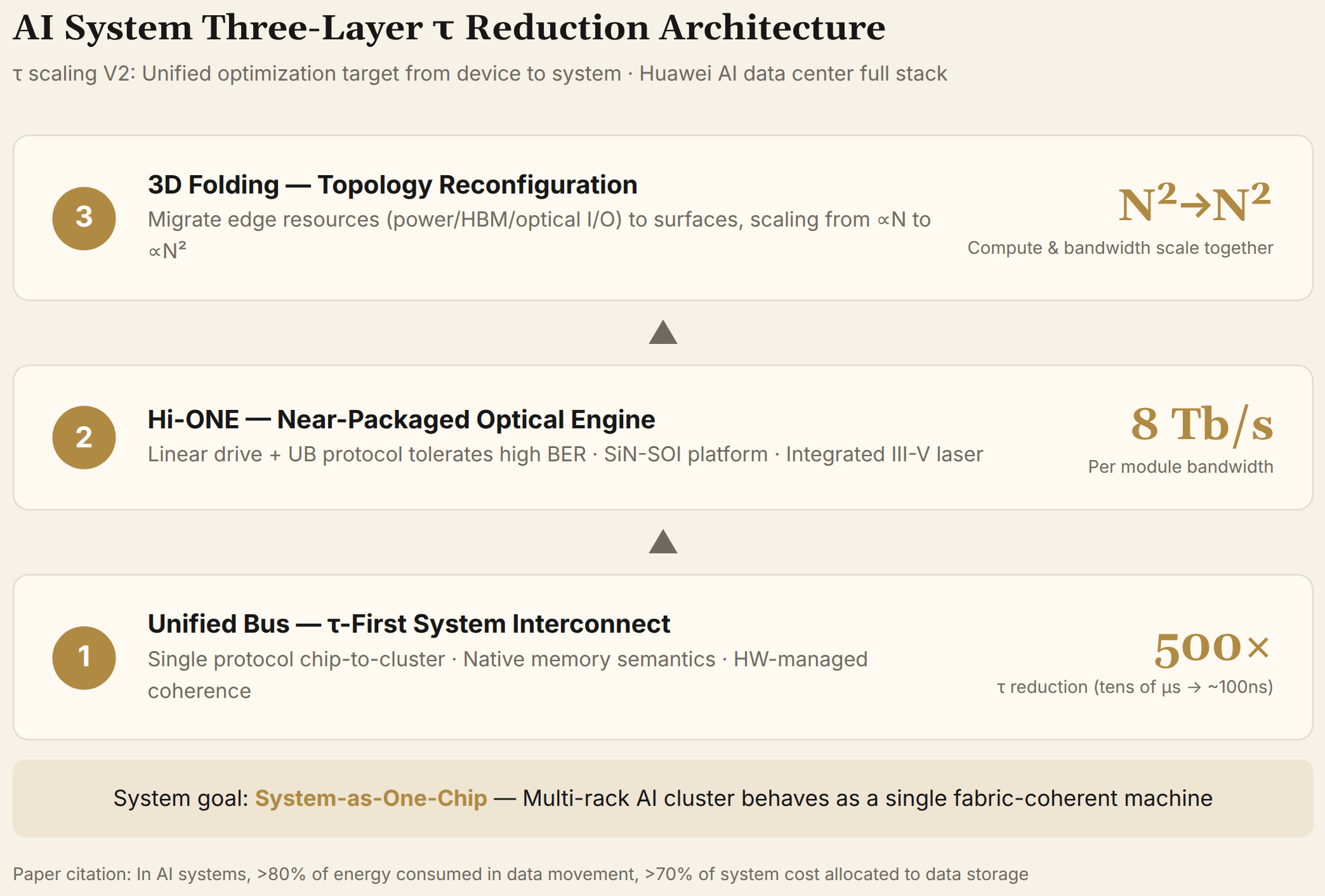
Layer 1: Unified Bus — τ-First System Interconnect
The traditional data path in multi-node AI architectures is a stack of protocol conversions: PCIe to host → NVLink/proprietary interconnect within rack → Ethernet/InfiniBand between racks → software stack for remote memory access. Each conversion adds latency, reduces reliability, and increases cost.
Unified Bus uses a single protocol covering both intra-rack and cross-rack communication — peer-to-peer, native memory semantics, hardware-managed coherence. Data movement is simplified to direct, conversion-free transfer at the memory semantic layer.
Measured result: end-to-end remote access latency drops from tens of microseconds (TCP/IP stack) to approximately 100 ns — a τ reduction of roughly 500×. This makes a multi-rack AI cluster behave asymptotally as "a single fabric-coherent machine" (Huawei internally calls this System-as-One-Chip).
Compared to InfiniBand's SHARP: SHARP performs reduction operations at the switch hardware level, reducing collective communication latency by 50-80%. UB takes a different approach — it does not optimize the efficiency of any single protocol layer, but eliminates protocol stack layers themselves. From a system architecture perspective, this shifts from "making each layer more efficient" to "needing fewer layers."
Layer 2: Hi-ONE — Near-Packaged Optical Engine
When communication latency is compressed to the 100 ns level by UB, the next bottleneck shifts to physical transport — copper is viable at SerDes rates up to 400 Gb/s, but at multi-Tb/s rates, copper becomes physically infeasible: SerDes hits shrink limits, cable volume becomes unacceptable, panel mounting fails, and thermal and power headroom is exhausted.
Hi-ONE (High-density Optical-interconnect-Node Engine) is a near-packaged optical engine technology platform from Hisilicon Optoelectronics. The V2 paper's presentation makes it appear new, but Hi-ONE has a longer public history:
Hi-ONE Product Family and Evolution Timeline
| Date | Event | Key disclosure |
|---|---|---|
| 2025.09 | IFOC 2025 | Hisilicon Optoelectronics CMO Xiong Qianjin unveils Hi-ONE platform, announces 7.2T SiPh NPO optical engine |
| 2026.01 | SPC Super Pod Conference | 7.2T engine completes channel-level performance verification and phased reliability testing, supports 224G NPO |
| 2026.05.28 | "xPO" Forum | Detailed breakdown: VCSEL 3.2T (32×112G) + SiPh 7.2T (36×224G) dual variants |
| 2026.05.29 | Optical Communications Forum | Xiong confirms Nebula optical interconnect in large-scale deployment across AI super-node networks |
| 2026.07.03 | τ scaling paper V2 | Module bandwidth upgraded from 7.2T to 8T, placed in τ scaling full-stack framework |
Hi-ONE covers two NPO optical engine variants on the same platform:
| Variant | Bandwidth | Channel config | Technology | Use case |
|---|---|---|---|---|
| VCSEL NPO | 3.2T | 32×112G | VCSEL array + ORFIC IC | Short reach (sub-100m) |
| SiPh NPO | 7.2T→8T | 36×224G | SiN-SOI + III-V high-power CW laser | Medium/long reach (100m+) |
Key technical features (from C114 reports and paper V2):
- Integrated shared light source: In-house III-V high-temperature CW laser, supporting full-temperature high-power output without external laser source
- SiN-SOI silicon photonics platform: Monolithic high-density integration of active and passive devices
- Linear drive scheme: No heavy DSP — uses analog equalization-enhanced driver + TIA, with UB protocol tolerating higher BER. The 800G SR8 LPO version reduces transport latency by over 90%
- StarSensor diagnostics: Minute-level link contamination/loose connection detection, centimeter-level fault localization — production network data shows most large model training failures originate from optical links, making this a direct pain point solution
- Multi-scenario compatibility: Pluggable / on-board / co-packaged all supported, multi-protocol (SR/DR/FR)
Hi-ONE's positioning from the V2 paper's perspective
This cross-layer trade-off is significant. Traditional optical module design pursues the lowest physical-layer BER, using DSP for heavy signal compensation. Hi-ONE deliberately relaxes BER requirements at the protocol layer, trading off physical-layer power and complexity — a concrete manifestation of τ scaling methodology in "protocol × physical" cross-layer optimization. Hi-ONE is not a standalone optical device but an organic component of the UB system.
Industry information reveals another dimension: Hi-ONE was announced as an independent NPO optical engine product in September 2025, and by May 2026 was confirmed to be "in large-scale deployment across AI super-node networks." This means the 8T figure in paper V2 may not be a theoretical projection but the latest iteration of a product specification already in deployment. The paper repositions an existing product within the τ scaling framework — upgrading it from "Hisilicon Optoelectronics' NPO product" to "the optical layer of the τ scaling architecture."
Compared to HGTECH's 3.2T NPO optical engine and Luxshare's NPO product matrix, Hi-ONE's differentiation lies in being the only optical engine explicitly co-designed with a system interconnect protocol (UB), rather than an independent module adapting to existing protocols. At the ODCC 2026 Summer Conference, Huawei simultaneously dissected the engineering challenges of 1024-lane NPO — Hi-ONE and those discussions are two sides of the same coin.
Layer 3: 3D Folding — Solving the N²-vs-N Dilemma
V2 presents a clean geometric argument for why 2.5D packaging inevitably hits a ceiling. This argument depends on no process parameter — it is purely a topological constraint, making it more compelling than empirical claims like "lithography is too expensive" or "we're hitting physical limits."
The N²-vs-N dilemma. In a 2.5D AI chip with side length N:
- Compute capacity ∝ N² (area)
- Bandwidth / interconnect / power ∝ N (perimeter — HBM stacks and SerDes line the edges)
Area grows faster than perimeter. The larger the chip, the wider the bandwidth gap that starves compute units. This cannot be closed by transistor-level improvements — it is a topological constraint.
The argument's power lies in its universality: no matter how fast transistors become or how dense HBM gets, as long as bandwidth resources are arranged along chip edges (2.5D fan-out), there is no escaping the N²-vs-N scissors gap.
3D Folding's solution: migrate edge resources to surfaces. Power enters from the bottom via backside power delivery (BSPDN), HBM stacks above logic layers through hybrid bonding, and optical I/O sits on the package surface through near-packaged Hi-ONE. Once these resources migrate from "edges" to "surfaces," their scaling law shifts from ∝ N to ∝ N² — growing in lockstep with compute capacity. The package is no longer "a logic chip surrounded by memory and SerDes" but "a vertically integrated stack where memory, interconnect, power, and logic all scale as N²."
Ascend Roadmap
The paper places AI accelerator evolution on the τ scaling timeline (chip codenames and dates from V2 paper; Lingqu versions and compute specs from Huawei Connect 2025):
- Ascend 910C (2025): Atlas 900 super-node, 384 cards, Lingqu 1.0
- Ascend 950 (2026 Q4): Atlas 950 super-node, 8192 cards, Lingqu 2.0, FP8 8 EFLOPS
- Ascend 990 (~2030): First introduction of LogicFolding in AI accelerators, 3D Folding becomes mainstream
- 2030→2035: Hardware integration density growth >100×
Key signal: LogicFolding lands in mobile first (2026), entering AI accelerators only around 2030. AI chips have more thermal headroom than phones, but much larger die areas make thermal density management more complex. This timing gap reflects Huawei's cautious expansion strategy for LogicFolding — validate in power-constrained scenarios first, then scale to larger compute chips.
4. The Re-fusion of Logic and Memory
Section 6 makes an easily overlooked but far-reaching judgment: logic and memory are moving from "deliberate decoupling" back to "re-fusion."
In the 8086 era, the industry deliberately decoupled processors from memory through standardized memory buses — two industries scaling independently, forming a massive memory market. Processors iterated rapidly under Moore's Law; memory evolved at its own pace (DDR generations → HBM), loosely coupled through standardized interfaces.
The AI era is reversing this trend. HBM, hybrid bonding, 3D stacked SRAM are all symptoms of the same trend: the cost of data movement has caught up with and even exceeded the cost of computation. The paper's data — >80% of energy consumed in data movement, >70% of system cost allocated to data storage in large AI clusters — quantifies this structural shift.
The paper judges that supply chain pricing power is shifting from logic vendors to memory and packaging vendors. This judgment is not about any single company but about industrial structure evolution — when "where data sits" matters more than "where computing happens" for system efficiency, the strategic weight of links controlling data movement paths (memory, interconnect, packaging) naturally rises.
This has direct implications for supply chain investment logic. If the physical fusion of logic and memory is an irreversible structural trend, then the strategic weight of HBM, advanced packaging, and hybrid bonding equipment will continue to rise — this is not cyclical fluctuation but structural reordering of the semiconductor value chain.
5. Honest Open Challenges
Section 7 lists five open challenges. The value of this section lies not in listing problems — any roadmap has "risk factors" — but in the directness of the language. The paper does not shy away from τ scaling's structural limitations.
EDA Tool Chain Gap
Existing EDA is designed for 2D — area, timing, and power optimized along three independent axes, with system τ emerging as a byproduct. Full-scale LogicFolding requires tool chains that treat multiple stacked active layers as a single continuous design entity, performing cross-layer placement and timing closure at cell-level granularity. Vertical interconnect parasitics on cross-layer paths, TSV keep-out zones (KOZ), and inter-wafer process variation interactions are not covered by traditional 2D-trained tools.
The paper acknowledges "preliminary internal tools have produced usable results," with methodology details to be published in coming months. The more critical signal is the paper's call: "a τ-native toolchain — open, multi-physics, and 3D-native — is the single most important enabling investment for the next decade." This is not product marketing but a signal to the entire EDA industry.
Inter-Wafer Process Variation
LogicFolding bonds wafers that may come from different batches or even different nodes. Inter-wafer variation in Vth (threshold voltage), drive current, and interconnect RC is significantly larger than intra-wafer variation, with the greatest impact on clock distribution and hold-time margin. Intelligent redundancy, adaptive compensation, and τ-aware sign-off flows are necessary countermeasures — but these are ongoing engineering investments, not one-time theoretical solutions.
Vertical Interconnect Overhead
Every hybrid bonding pad and TSV has finite resistance and capacitance cost. LogicFolding must prove a simple inequality layer by layer: post-bonding τ (shortened wire delay) > bonding overhead τ (RC introduced by vertical interconnect). The paper notes that mobile critical paths and memory have passed this threshold, but thresholds differ by workload and shift as bonding pitch shrinks.
Energy: The Limit of a Time Law
This may be the most fundamental constraint. The paper states directly: "τ is a time law, not a joule law." A super-node that is 10× faster but consumes 10× more energy violates no scaling principle but exceeds grid capacity.
τ scaling therefore requires an energy companion: memory-semantic interconnects eliminating protocol stack overhead, near-packaged/co-packaged optics reducing pJ/bit, backside power reducing IR drop loss, in-memory/near-memory computation shortening data transport distances, and data-center-scale DVFS (converting τ headroom into power savings — the same principle as smartphones using DVFS to extend battery life, scaled to gigawatt-class). The paper notes: τ headroom itself, when allocated to energy-saving directions, provides energy margin. This is a positive feedback — τ optimization creates headroom that can feed back into energy constraints.
Benchmarking
Existing benchmarks (Linpack, MLPerf, SPEC) are designed for the "single scalar" era. The τ scaling industry needs τ-profile benchmarks — vectorized metrics exposing each layer's dominant τ and remaining headroom. The paper's judgment is brief but precise: the layer where the dominant τ resides is, by definition, the next investment priority.
6. Application Acceleration Factors
The paper provides, for the first time, a classification of τ reduction rates across application domains:
| Application | Annual scaling factor α | Logic |
|---|---|---|
| Mobile devices | ~1.3 | Power and thermal constraints |
| Autonomous driving | ~1.5 | Safety-critical real-time requirements |
| AI Token generation | up to ~10 | Throughput directly equals economic value |
The generational rule is τ_{n+1} = τ_n / α. Larger α means more τ reduction per generation. Mobile's α ≈ 1.3 means ~23% annual τ reduction; AI's α up to 10 means certain dimensions can see 90% reduction in a single year.
This classification explains why Huawei prioritizes AI system-level τ reduction investment — Lingqu, Hi-ONE, super-nodes — rather than spreading across other scenarios. AI Token throughput's annual scaling rate is nearly 8× that of mobile, and every layer of τ reduction yields far higher marginal returns than other applications. These numbers also answer a question external observers frequently ask: "Why doesn't Huawei apply LogicFolding to AI chips first?" The answer lies in the α differential — AI system τ reduction headroom is much larger and does not depend on LogicFolding alone; Lingqu UB and Hi-ONE system-level gains are already substantial. LogicFolding enters AI accelerators around 2030, when UB and Hi-ONE marginal τ gains begin to diminish and a new round of device-level folding is needed to carry the baton.
7. Six Years of Accumulation, Ten-Year Outlook
Section 8 provides a periodic summary. From May 2020 to May 2026, Huawei Semiconductor designed and mass-produced 381 chips across mobile, AI, automotive, industrial, and infrastructure markets. The paper supports τ scaling's validity with measured results at three levels:
- Device and circuit level: transistor density advancing from 155 toward 400+ MTr/mm²
- Chip level: LogicFolding validated sustained improvements in critical-path frequency, energy efficiency, and density at a fixed process node
- System level: UB and Hi-ONE demonstrated that hundreds-of-microseconds communication τ can be compressed to hundreds of nanoseconds, enabling multi-rack AI clusters to behave as a single coherent machine
The 381-chip figure is itself a form of argument. τ scaling is not a theoretical model in a paper — it is a methodology validated across 381 mass-produced chips over six years. From a statistical perspective, if τ scaling only worked on a few products, it could be dismissed as anecdotal; 381 chips spanning multiple industries demonstrate industrial-grade reproducibility.
8. Assessment
Significance for Semiconductor Evolution Framework
Moore's Law established a "single-variable scaling" framework — smaller transistors → everything improves. This framework's simplicity is why it dominated the industry for sixty years. But it came with a cost: device, circuit, chip, and system layers each optimized independently, with system-level τ emerging as nobody's responsibility — a "residual."
Dennard scaling once bridged device and circuit — "proportional scaling maintains constant electric field" gave device physicists and circuit designers a common language. When Dennard failed around 2005, that bridge broke. τ scaling attempts to build a larger bridge — not connecting adjacent layers but spanning device to system. Whether it succeeds depends on how many industry participants actually adopt τ as a cross-layer collaboration metric in the next five to ten years.
Practical Impact on the Competitive Landscape
For Huawei: The paper extends the Ascend roadmap to 2035 — Ascend 990 introduces LogicFolding, 100× hardware integration density growth. Lingqu UB's ~100 ns latency and Hi-ONE's 8 Tb/s module bandwidth provide hard data for evaluating Huawei super-node performance.
For semiconductor equipment: The 1.5 μm hybrid bonding pitch is in mass production. Domestic bonding equipment (NAURA Qomola HPD30, Piotech W2W production models) warrants continued tracking — the paper's disclosure indirectly confirms this production line's maturity.
For memory: If the logic-memory re-fusion judgment holds, HBM and advanced packaging strategic weight will continue to rise. Memory and packaging are no longer "supporting actors for logic chips" but are becoming system performance determinants.
For export controls: The paper explicitly states "competitive performance no longer requires perpetual residence on the leading edge of lithography." If this judgment is validated by industry practice within 5-10 years — i.e., system performance can continue improving without the most advanced lithography — then the effectiveness of export control strategies built around restricting advanced process access will be systematically eroded.
9. Frontier Comparison: Catching Up, Innovating, and Route Divergence
τ scaling was not born in a vacuum. The global semiconductor industry is shifting toward 3D and system-level optimization, but each player's path choices differ fundamentally. This section places Huawei's progress in global coordinates for item-by-item comparison.
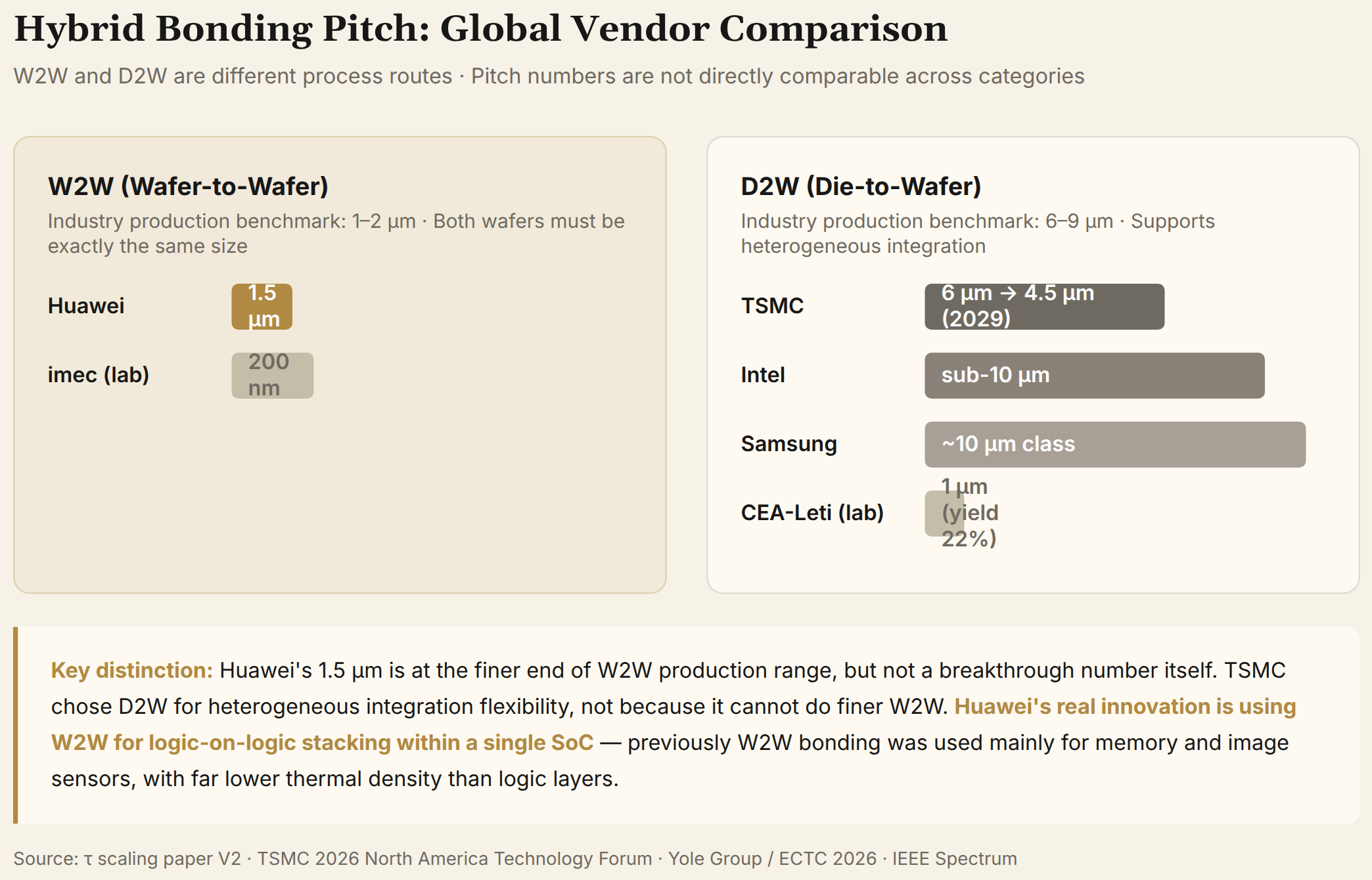
Hybrid Bonding Pitch: Huawei Leads, but Differently
Hybrid bonding pitch is the hardest metric in 3D integration. Current global status:
| Vendor | Technology | Bonding mode | Current production pitch | Roadmap target |
|---|---|---|---|---|
| Huawei | LogicFolding | W2W | 1.5 μm | Toward sub-1 μm / gear ratio ≈1 |
| TSMC | SoIC-X | D2W | ~6 μm | 4.5 μm (2029) |
| Intel | Foveros Direct | D2W | sub-10 μm | No clear sub-5 μm roadmap |
| Samsung | I-Cube4 / X-Cube | D2W | ~10 μm class | Following strategy |
This table requires a critical caveat: W2W and D2W are different process routes, and pitch numbers cannot be directly compared across categories. According to Yole Group analysts at ECTC 2026, current industry production benchmarks are: W2W 1-2 μm, D2W 6-9 μm. W2W naturally achieves finer pitches — full-wafer alignment precision far exceeds die-by-die placement. Huawei's 1.5 μm sits at the finer end of W2W production range, but this is not a breakthrough number in itself.
TSMC chose D2W not because it cannot do finer W2W, but because customer products require heterogeneous integration — flexible combination of different-sized, different-node dies. D2W supports this flexibility while W2W requires both wafers to be exactly the same size.
Huawei's real innovation is not the pitch number but using W2W for logic-on-logic stacking within a single SoC. W2W hybrid bonding was previously used primarily for memory stacking (HBM) and image sensors — scenarios with far lower thermal density than logic layers. Huawei uses W2W between active logic layers within the same SoC, simultaneously solving thermal management, clock distribution, and cell-level critical-path folding design methodology. This is the truly unprecedented work in paper V2.
At the laboratory level, imec demonstrated 200 nm W2W pitch at ECTC 2026 (not production), and CEA-Leti showed 1 μm D2W pitch (yield only 22%, not production). The gap between production and laboratory remains significant.
Backside Power Delivery: Huawei Not Yet, Industry Already Shipping
Backside power delivery network (BSPDN) moves power lines from the wafer frontside to the backside, freeing frontside space entirely for signal routing. This is essential for 2nm and below nodes.
| Vendor | Technology | Status |
|---|---|---|
| Intel | PowerVia | 18A in production (2025) |
| TSMC | Super Power Rail (A16) | Production late 2026, more complex than Intel |
| Samsung | BSPDN (SF2Z) | 2027 production |
| Huawei | — | Paper does not mention |
The paper mentions backside power when describing 3D Folding, but as a future architectural direction, not an existing achievement. In Kirin 2026's LogicFolding implementation, the paper does not mention backside power delivery.
This means Huawei's device-layer τ reduction toolbox is missing an important weapon. Intel 18A + PowerVia measured 25% frequency improvement at equivalent voltage, or 36% power reduction. If Huawei can eventually overlay BSPDN on LogicFolding, there is theoretically an additional layer of frequency/power improvement — but when this capability arrives depends on domestic advanced process backside power maturity.
System-Level Interconnect: Two Philosophies
In AI data center system-level interconnect, Huawei and NVIDIA represent fundamentally different philosophies.
NVIDIA's path: continuously expanding the NVLink domain (NVL72 → NVL144 → NVL576 → NVL1152), gradually introducing CPO for scale-up (Rubin Ultra NVL576 already uses CPO for cross-rack optical interconnect, Feynman NVL1152 will be all-CPO), with a clear layered protocol stack: NVLink (scale-up) + InfiniBand/Ethernet (scale-out).
Huawei's path: Unified Bus uses a single protocol covering chip-to-rack-to-cluster scale, eliminating protocol conversion overhead. UB's ~100 ns remote access latency is on the order of NVLink intra-rack latency, but must cover far greater physical distances.
The divergence: NVIDIA's layered stack allows each layer to be independently optimized (NVLink for ultra-low latency, Ethernet for high bandwidth and standardization economics), at the cost of cross-layer conversion overhead. Huawei's UB eliminates conversion overhead through unified semantics, at the cost of requiring the protocol to simultaneously satisfy scale-up's ultra-low latency and scale-out's massive scalability. Which path ultimately wins depends on whether UB can maintain ~100 ns latency at thousand-card scale — this is currently paper data requiring real deployment verification.
Optical Interconnect: CPO vs NPO Route Race
Huawei's Hi-ONE and NVIDIA's Spectrum-X Photonics represent two engineering paths for optical interconnect:
| Dimension | NVIDIA Spectrum-X Photonics | Huawei Hi-ONE |
|---|---|---|
| Position | Scale-out CPO Ethernet switch | Scale-up near-packaged optical engine |
| Interconnect target | Switch-to-switch (spine-leaf) | Chip-to-chip (within UB fabric) |
| Bandwidth | 400 Tb/s switch capacity | 8 Tb/s per module |
| Signal processing | Traditional DSP (programmable) | Linear drive (analog equalization) |
| Protocol layer | Ethernet + RoCEv2 | UB native memory semantics |
| Production status | Announced "in production" (5/31) | Paper does not give production date |
NVIDIA's CPO serves the scale-out network — letting Ethernet switches break through electrical signal panel density limits. Huawei's Hi-ONE serves the scale-up fabric — migrating UB protocol's physical transport from copper to light. These are not direct competitors but solve optical interconnect problems at different system hierarchy levels.
The deeper difference is signal processing philosophy. NVIDIA chose traditional programmable DSP — mature but power-hungry. Huawei chose linear drive — lower power but signal fidelity depends on UB protocol's fault-tolerant design. This is a concrete manifestation of τ scaling methodology — relaxing BER requirements at the physical layer to reduce power, optimizing for total system τ. But it also means Hi-ONE cannot be used independently — it must be co-designed with the UB protocol stack.
Sequential 3D: Where Is the Real Ceiling?
LogicFolding uses W2W hybrid bonding to achieve two active logic layer stacking at 1.5 μm pitch. But the paper itself acknowledges that Sequential 3D (S3D) — building transistor layers sequentially on the same wafer — is theoretically superior.
S3D advantages: inter-layer interconnect density 3-4 orders of magnitude higher than W2W bonding (lithographic precision vs bonding precision); no need for two wafers; theoretically unconstrained by bonding pitch.
S3D bottlenecks: performance degradation of lower-layer devices under thermal budget constraints — upper-layer transistor processing temperature must stay below ~600°C; imec/Leti's CoolCube has validated logic-on-logic stacking in the lab but remains far from production; globally, S3D production timeline is post-2030.
The paper's judgment: LogicFolding's W2W bonding is a commercially viable intermediate route. Once S3D matures, the design methodology (critical-path folding, gear ratio optimization) can transition smoothly.
LogicFolding's theoretical ceiling depends not on bonding pitch but on thermal management. Two active logic layers have far higher power density than memory stacks — imec simulations show 4-layer HBM-on-GPU reaching 142°C without extreme optimization. Stacking 3-4 logic layers will make thermal density issues worse. The paper's response is thermal-aware partitioning, but no specific solution is offered.
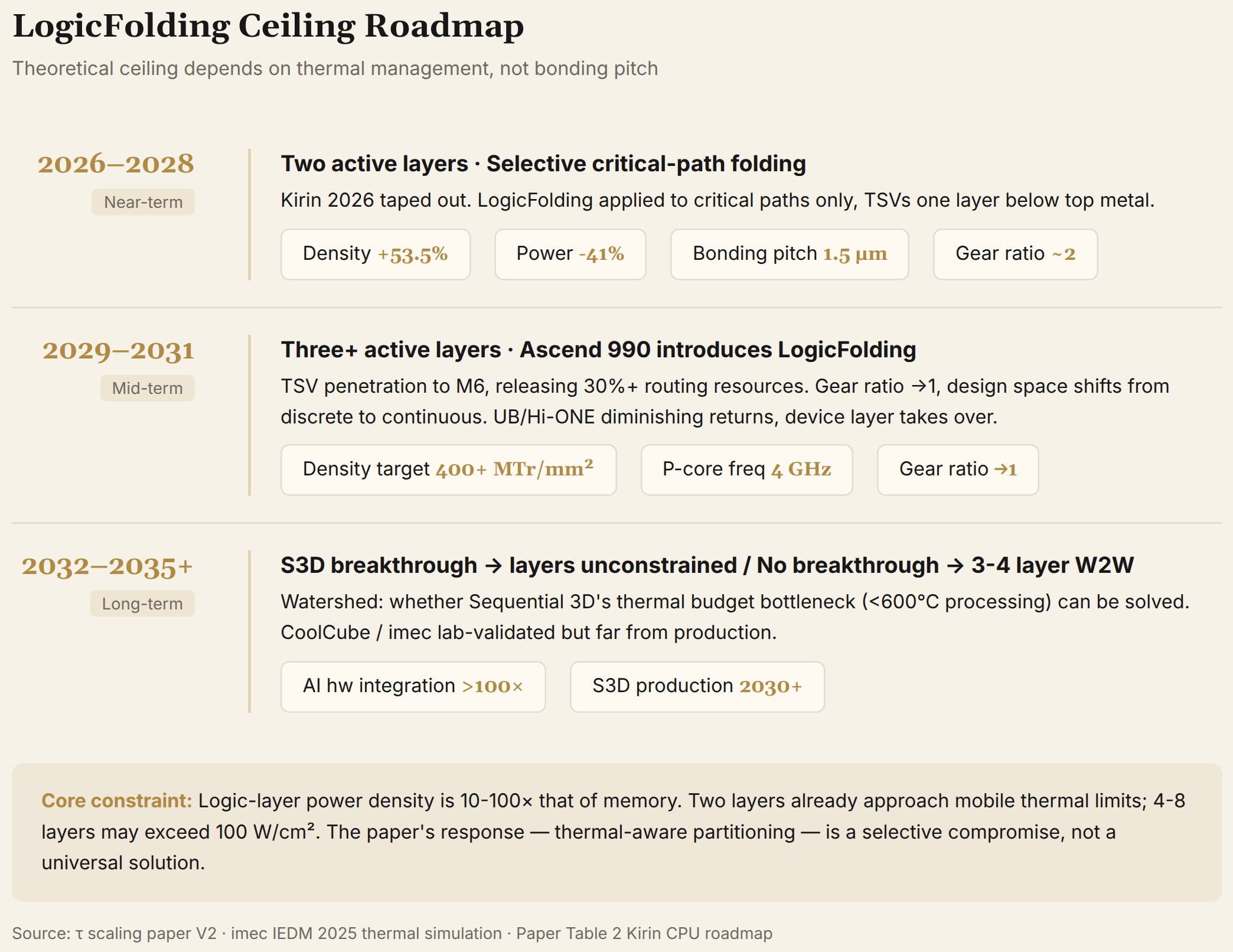
Ceiling summary:
- Near-term (2026-2028): Two active layers, selective critical-path folding. Density +55%, power -41%
- Mid-term (2029-2031): Three+ active layers, TSV penetration to M6, gear ratio →1. Density 400+ MTr/mm²
- Long-term (2032-2035+): If S3D breaks through thermal budget, layer count unconstrained by bonding; if not, limited to 3-4 layer W2W
Route Divergence: Three Unanswered Questions
Question 1: Can system-level optimization permanently substitute for advanced lithography?
The paper's core claim is that competitive performance no longer requires leading-edge lithography. But this claim has a precondition: system-level τ reduction's marginal returns do not diminish. If UB latency hits diminishing returns after compression to 100 ns, or Hi-ONE bandwidth density hits physical limits, system-level optimization will need a new round of device-level breakthroughs. The paper places Ascend 990's (~2030) introduction of LogicFolding at precisely when UB/Hi-ONE marginal returns begin to diminish — this is not coincidental.
Question 2: Who gets EDA right first?
LogicFolding requires 3D-native, multi-physics, cell-level granularity EDA tool chains. The paper admits Huawei has only "preliminary internal tools." Globally, Synopsys/Cadence dominate 2D EDA with 3D IC tools still early; TSMC's 3DFabric Alliance is building its own 3D design ecosystem; Peking University has published a "true 3D" EDA prototype. Whoever first achieves a mature τ-native 3D EDA tool chain will accelerate design closure for LogicFolding-class technologies. This is the largest uncertainty on Huawei's path.
Question 3: Is thermal management the ultimate physical ceiling?
Two active logic layers' thermal density already approaches mobile thermal limits. AI accelerators have more thermal headroom (liquid cooling, larger die area), but when LogicFolding enters AI chips and stacks to 3-4 layers, power density may exceed 100 W/cm². The paper's proposed solution — thermal-aware partitioning and avoiding folding high-power circuits — means LogicFolding is not applied universally but selectively under thermal constraints. Whether this constraint becomes an insurmountable physical wall at 4-8 layers remains unanswered.
Verification Points to Track
- Kirin 2026 production measurements: Paper labels status as "Silicon" (taped out); actual thermal performance, yield, and daily-use power after fall 2026 launch will be the first external validation
- Ascend 950 super-node real deployment: Training performance, inference throughput, and stability after Q4 2026 launch — especially whether UB remote access latency reaches the paper's claimed ~100 ns under real workloads
- Hi-ONE production timeline: Paper provides no specific production date — a gap requiring tracking
- EDA tool chain openness progress: Paper calls for open collaboration, but specific partnership models and scope remain undefined
Source note: This article is based on He Tingbo's paper "A Time Scaling Theory for Multi-Layer Electronic Systems" V2 (ChinaXiv:202605.00224v2, 2026-07-03, accepted by Science China). Kirin 2026 measured data, gear ratio theory, Hi-ONE specifications, N²-vs-N geometric argument, and Ascend roadmap are first disclosed in paper V2. Ascend compute specs and Lingqu versions are from Huawei Connect 2025. Hi-ONE product details are from Hisilicon Optoelectronics presentations at IFOC 2025 (September 2025), SPC Super Pod Conference (January 2026), and the "xPO" Forum (May 2026), reported by C114. Industry comparison data is from TSMC 2026 North America Technology Forum, Intel Foveros Direct technical brief, IEEE Spectrum / ECTC 2026, TrendForce, and Tom's Hardware. Not investment advice. Data as of July 3, 2026.