
Can the AI Supply Chain Digest $887 B?
TrendForce's August 3 report: nine major CSPs' 2026 capex reaches $886.7 billion (+90% YoY), and $1.32 trillion in 2027 (+49%). The global semiconductor market is approximately $600 billion. Nine companies' annual investment = 1.5× global chip output.
Everyone is staring at "whether AI can pay for itself." Palantir Q2 revenue +93%, Snap DAU +5%, both surged after-hours. Analysts say "AI revenue now covers depreciation for the first time." But capital markets are asking a P&L question. The physical layer has a colder one: even if every dollar converts to orders, can the supply chain deliver on time?
The answer is no.
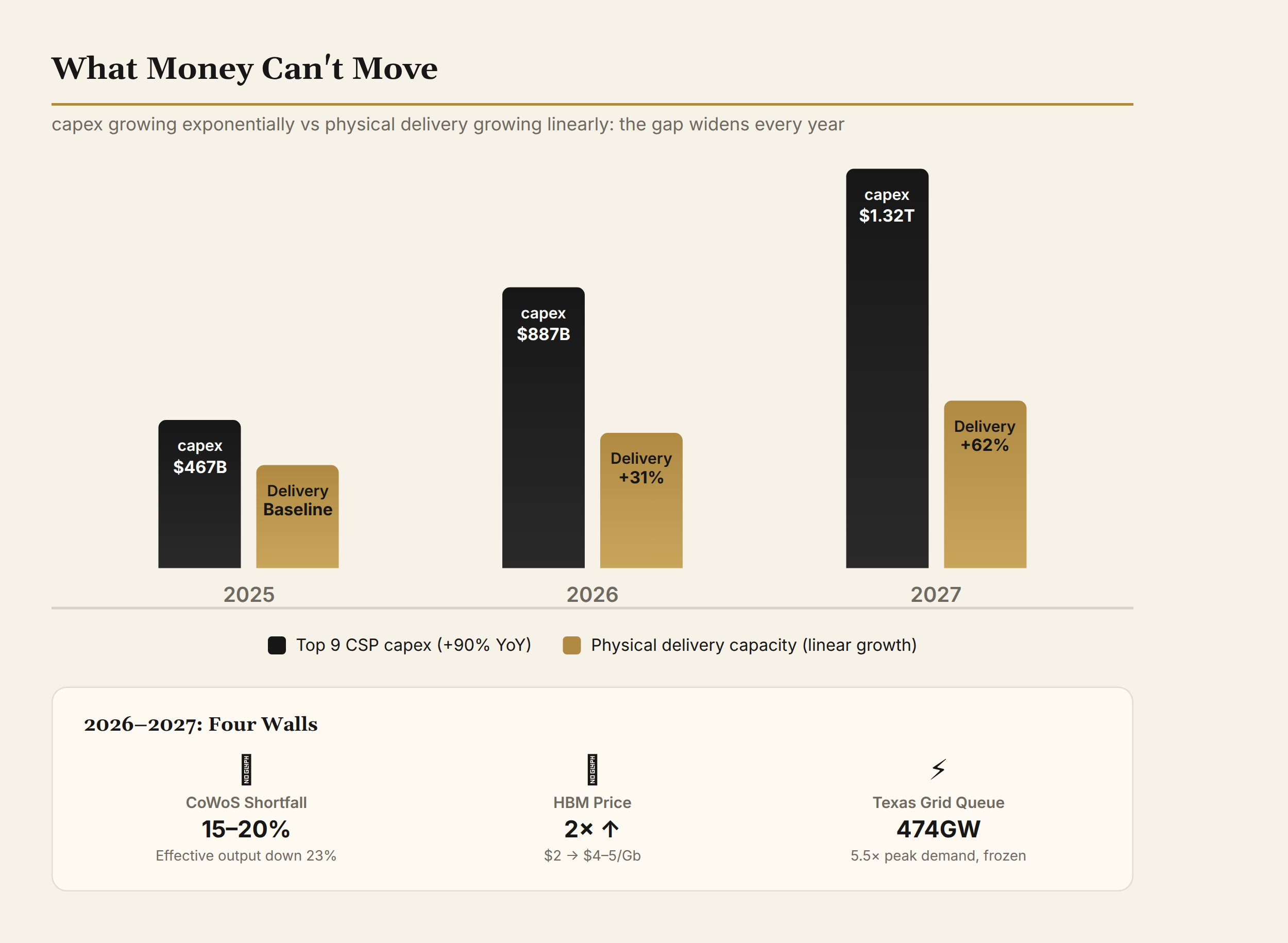
The problem is mathematical. Capex grows exponentially—$467 billion in 2025, $886.7 billion in 2026, $1.32 trillion in 2027, a 2.8× increase over three years. But physical delivery capacity is linear, and in some segments sub-linear. A fab takes 2–3 years from groundbreaking to production. A substation takes 3–7 years from siting to energization. A nuclear reactor takes 5–10 years from blueprint to criticality. The gap between the two curves widens every year. By 2026 the gap is visible to the naked eye: CoWoS industry-estimated shortfall of 15–20%, HBM prices doubled, and the Texas grid has frozen 474 GW of interconnection applications.
This gap is the AI industry's largest systemic risk. The four walls below each tell the same story: the parts money can't move are what truly determine the landscape.
I. CoWoS: A Bottleneck Accelerating Itself
Start with the surface numbers. TSMC's CoWoS monthly capacity: 10,000 wafers in 2022 → 140,000 by end of 2026 → an estimated 200,000 in 2027. A 20× increase in five years. Over the same period, demand rises from approximately 1.38 million wafers (wafer-equivalent) in 2024 to approximately 2.69 million in 2027 (Morgan Stanley forecast). It looks like supply and demand are racing.
In reality, supply is treading water.
The Measurement Trap
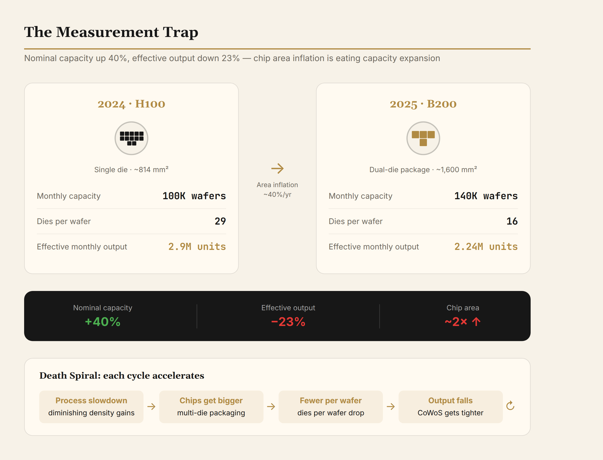
The industry reports capacity in "wafers"—how many 300 mm wafers processed per month. Customers compete for "dies"—how many usable chips come out per month. The conversion factor is die area, and that area is inflating at roughly 40% per year.
In 2024, one 12-inch wafer yielded 29 H100 dies. In 2025, the same wafer yields only 16 B200 dies—the B200 is a dual-die design, with each die approximately 814 mm² (comparable to the H100 and near the reticle limit of 858 mm²). Two dies co-packaged bring the combined area to approximately 1,600 mm², halving the effective output per wafer. Net effect:
- 2024: 100,000 wafers × 29 dies = 2.9 million H100 dies/month
- 2025: 140,000 wafers × 16 dies = 2.24 million B200 dies/month
Nominal capacity grew 40%; effective output fell 23%. That is why CoWoS gets tighter the more it expands.
The Feedback Loop
The question "why must chips get bigger" leads to one answer: the single-die scaling path has run its course.
From 5 nm to 3 nm to 2 nm, the transistor density improvement curve is flattening. Each process node doubles R&D cost (2 nm costs approximately $30 billion), but density gains have dropped from 1.7× (7→5 nm) to 1.15× (3→2 nm). The number of transistors a single die can hold at advanced nodes is still rising, but with diminishing returns and exploding cost.
The way out is multi-die co-packaging. Multiple compute dies and HBM stacks are placed on the same interposer, using advanced packaging to substitute for process scaling. The B200 co-packages two dies. According to supply-chain analysis, Rubin Ultra plans to co-package four compute dies, pushing package area to 7.5–8× the reticle limit.
This is a positive feedback loop: process scaling stalls → chip area is forced to grow → dies per wafer drop → CoWoS effective output falls → supply tightens → demand spills to alternatives. Each turn of the loop accelerates, because the next GPU generation is always larger than the last.
The loop stops only when one of two conditions is met: either process scaling re-accelerates (GAA below 2 nm / 2D materials are still 3–5 years away), or the packaging paradigm shifts (from silicon interposer to panel-level, i.e., CoPoS).
Can CoPoS Break the Deadlock?
TSMC's own answer is CoPoS (Chip-on-Panel-on-Substrate): replace round silicon wafers with square glass panels, jumping material utilization from under 70% to 90%+. The Chiayi AP8 pilot line is under construction, targeting mass production in 2028–2029.
CoPoS must clear three hurdles.
The first is warpage control. Glass has a coefficient of thermal expansion (approximately 3.0 ppm/K) close to silicon (2.6 ppm/K) and far better than organic substrates (16 ppm/K)—this is glass's core advantage. But glass panels behave fundamentally differently from silicon under high-temperature bonding, and nearly all existing CoWoS process equipment must be redesigned from scratch. TSMC has a decade of process data on CoWoS; on CoPoS, it has zero.
The second is TGV (Through-Glass Via). The TSV (Through-Silicon Via) process on silicon interposers has matured to 1 μm diameter. Glass vias currently struggle to reach even 10 μm, while next-generation AI chips require interconnect densities that demand at least 5 μm. Both laser drilling and plasma etching routes remain in the laboratory phase.
The third is yield. CoWoS-L yield is 98%, the product of ten years of iteration. CoPoS initial yield will likely sit in the 50–60% range. Assume 60% yield: a panel-level package at 8× reticle area would have a per-die cost 1.5–2× that of CoWoS-L—even with higher material utilization. Yield ramp requires at least 2–3 years, and reaching 90%+ would take until 2030–2031.
So CoPoS is the right direction, but it cannot help before 2028. The 2026–2027 CoWoS gap can only be filled by alternatives within the existing framework.
Substitution Is Already Happening
SemiAnalysis's July 2026 report states that Google's next-generation TPU "Humufish" will adopt Intel EMIB-T packaging instead of TSMC CoWoS. If true, this is the first time since 2012 that CoWoS has been bypassed by a hyperscaler's flagship AI chip. Ming-Chi Kuo's analysis adds an important caveat: EMIB-T validation yield is approximately 90%, still short of the 98% needed for mass production, and Google is simultaneously querying TSMC for Humufish main compute die tape-out costs—the plan is not fully locked. Intel's EMIB-T parameters presented at IEEE ECTC 2026—25 μm bump pitch, 120×120 mm package, 9× reticle area—are already on par with CoWoS-L. The cost structure is lower: EMIB does not require a full silicon interposer, using only local silicon bridges (LSI) for high-speed inter-die signals while routing the rest through an organic substrate, reducing material cost by 30–40% versus CoWoS.
Reportedly, NVIDIA's next-generation Feynman GPU will also adopt a dual-source CoWoS + EMIB strategy. AMD's next-generation MI series is evaluating EMIB. Industry analysts broadly estimate the CoWoS supply-demand gap at 15–20%, expected to persist through 2028.
What does the gap mean? Using 2027 global CoWoS demand of approximately 2.69 million wafers (wafer-equivalent, Morgan Stanley forecast), a 15–20% shortfall translates to approximately 400,000–540,000 wafers, or roughly 6.4–8.6 million B200-equivalent dies per year. This is an industry-wide shortfall—Google, AMD, AWS, and Chinese CSPs are all competing for the same capacity. For NVIDIA, which depends heavily on CoWoS, the gap means delivery lead times for a significant portion of incremental orders will be extended.
II. HBM: From Market Pricing to Rationing
HBM's problem is deeper than CoWoS. CoWoS is a capacity bottleneck that can be gradually relieved through investment and alternative technologies. HBM is a resource bottleneck—the DRAM wafer capacity it consumes cannot be expanded without limit.
The 3× Law
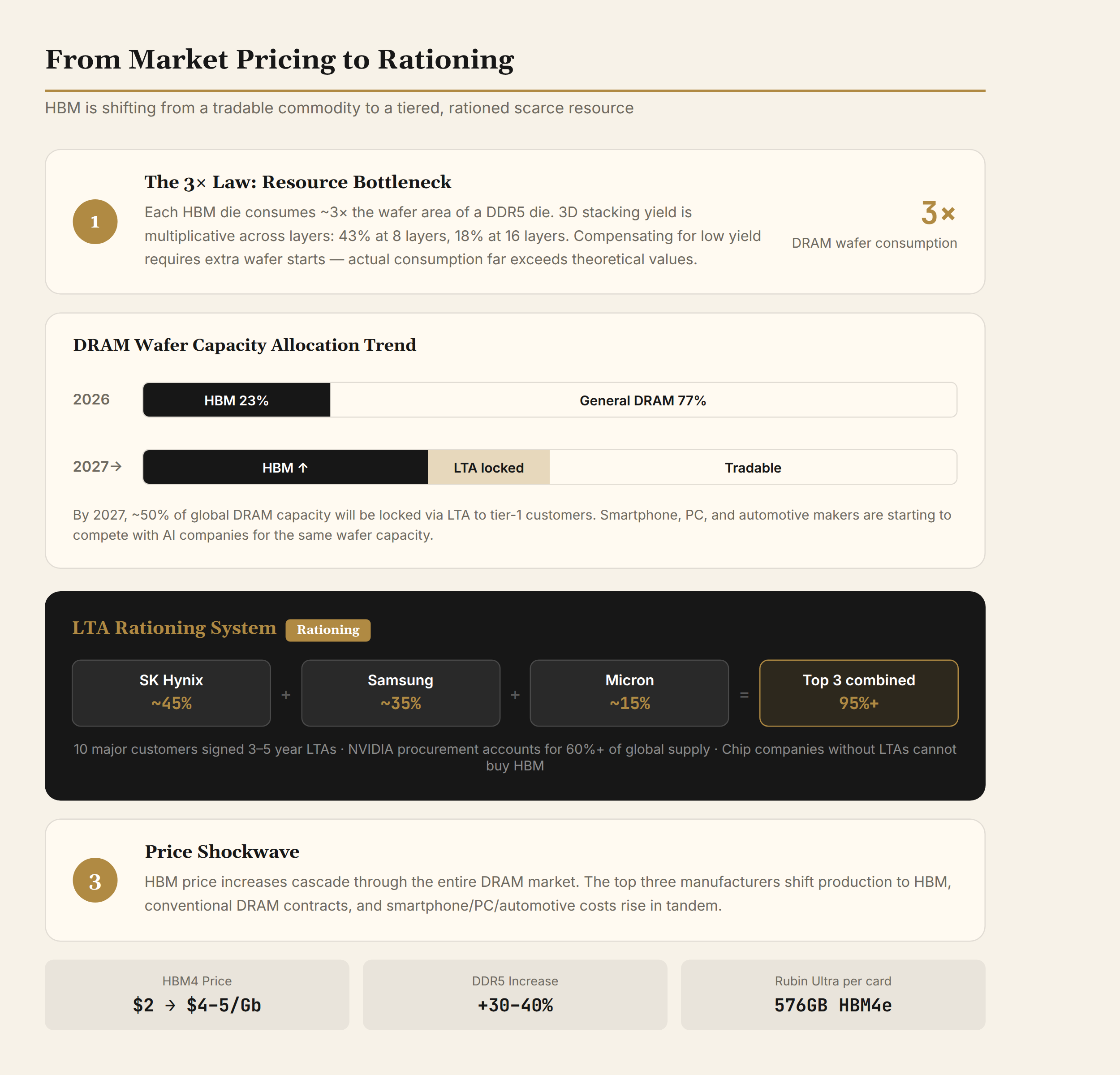
Producing one HBM chip consumes the wafer area of approximately three DDR5 chips. The reason is straightforward: HBM requires vertically stacking 8–16 DRAM dies, each of which must be individually fabricated, tested, and bonded. The yield of a 3D stack is the product of individual layer yields—assuming 90% per-layer yield, an 8-layer stack yields only 43% (0.9^8), and a 16-layer stack only 18% (0.9^16). To compensate for low yield, more wafers must be started, making actual wafer consumption far exceed theoretical values.
DigiTimes' July report revealed a broader lock-in effect: by 2027, approximately 50% of total global DRAM capacity will be locked to tier-one customers through LTAs—not just HBM, but also server DDR5 and other specialty DRAM secured by large customers through long-term agreements. In 2026, HBM already accounted for approximately 23% of global DRAM wafer capacity (TrendForce data), and as the Big Three memory makers convert more lines to HBM, this share is expected to keep climbing. For smaller buyers, the available spot-market supply of commodity DRAM is shrinking rapidly—smartphone makers, PC OEMs, and automotive electronics suppliers are all now competing with AI companies for the same wafer capacity.
The result: HBM4 prices have risen from approximately $2/Gb to $4–5/Gb (DigiTimes, July 2026 report). But the price transmission goes far beyond HBM itself. The Big Three memory makers are converting more and more DRAM lines to HBM, contracting commodity DRAM supply. DDR5 prices have been rising since end of 2025, up approximately 30–40% in 2026. Memory procurement costs for smartphones, PCs, and automotive electronics follow suit. Every additional HBM die consumed by an AI data center sacrifices the wafer capacity of three DDR5 chips—a cost that appears on no AI company's financial statement. It is distributed across the bill of materials of every smartphone, every PC, and every connected car worldwide.
Rationing Economics
On July 29, SK Hynix announced 3–5 year long-term supply agreements (LTAs) with 10 major customers. Samsung and Micron followed. The three companies collectively cover more than 95% of global HBM capacity.
The LTA regime has changed HBM's pricing mechanism. The traditional semiconductor cycle: prices rise → capacity expands → oversupply → prices fall. LTAs break this cycle—large customers lock quantity and price for 3–5 years, capacity expansion is pre-allocated, and the remaining tradeable HBM supply is minimal. This is no longer market pricing. This is rationing.
Rationing priority is set by NVIDIA. NVIDIA's HBM purchases account for 60%+ of global supply, and its LTA suppliers (primarily SK Hynix) take the highest-quality capacity. AMD, Google, and AWS in-house chip teams get the second tier. Further down, mid-size chip companies and enterprise AI teams find that even with money, they cannot buy HBM.
This structure has a second-order effect: HBM availability is becoming a barrier to entry in the AI industry. New entrants, even with chip design capabilities, cannot mass-produce without HBM. After 2027, AI chip companies without LTAs may find they have designed chips with no memory to run them on.
Demand Is Still Accelerating
The Rubin GPU carries 288–384 GB of HBM4 (per Bank of America report). Rubin Ultra V300 is equipped with 576 GB of HBM4e (Bank of America estimate). The B200 carries 192 GB. That is roughly a 3× leap between two generations—per-chip HBM demand is rising, but the real issue is scale.
Order-of-magnitude sense: Rubin Ultra at 576 GB HBM4e per GPU. If NVIDIA ships millions of Rubin-class GPUs in 2027, at an average of 400 GB each, total demand reaches hundreds of millions of GB. Whether the combined annual HBM capacity of the Big Three memory makers can cover this volume is one of the biggest open questions for 2027.
And that is just NVIDIA. Add AMD, Google TPU, AWS Trainium, and Chinese CSP in-house chips, and 2027 HBM demand will most likely exceed the total capacity of the three memory makers.
III. The Grid: The Longest Critical Path
The Load Curve Problem
Of the 474 GW of interconnection applications queued at ERCOT in Texas, 90% are data centers. Governor Abbott ordered a comprehensive audit and freeze on August 3.
The 474 GW figure is staggering enough on its own—Texas peak grid demand is approximately 85 GW (measured record peak, summer 2025), making the queue 5.5× the peak. But the deeper problem lies in load characteristics.
Traditional grid planning assumes diversified loads: residential demand peaks in morning and evening, industrial demand is primarily daytime, commercial demand is primarily weekdays—different load types offset each other's peaks, and grid capacity can be designed below the sum of all users' individual peaks. Data center load curves are completely different: constant high-power operation 24/7, no peak-sharing, no seasonal decline. A data center's load has zero diversity—every second is peak. This means the grid must provide 1:1 generation capacity plus reserve margin (typically ~15%) for data centers, with no opportunity for load diversification as with residential demand.
If all 474 GW of queued data center load at ERCOT were energized, that single category would far exceed the approximately 1.3 TW of total installed U.S. generation capacity (estimated from EIA capacity data). Physically impossible.
The Hidden Bottleneck: Transformers
Even if grid approvals go through, data centers face an even more concealed bottleneck: transformers.
Large data centers need 500 MVA-class transformers to step down grid high voltage (345 kV/500 kV) to distribution voltage. Industry research data shows that large power transformer (LPT) delivery lead times have stretched from approximately 30–40 weeks in 2019 to 120–200+ weeks in 2024–2026 (approximately 2.3–3.8 years). Manufacturers capable of producing 500 MVA+ transformers are globally scarce—Hitachi Energy (formerly ABB Grid), Siemens Energy, Mitsubishi Heavy Industries, HD Hyundai Electric, GE Vernova, TBEA, and a handful of others divide the vast majority of capacity. Building a new large transformer factory requires approximately $500 million–$1 billion and 3 years of construction; capacity expansion barely keeps pace with demand.
Transmission cable, switchgear, and circuit breakers are similarly tight. One way to put it: for a new large data center in the U.S., from transformer order to energization—if the transformer hasn't been ordered yet, add 4 years.
The Energy Solution Timeline
SMRs (Small Modular Reactors) are the most discussed solution. Valar Atomics just closed a $1 billion Series B (Sequoia-led, $6 billion valuation), and the Ward 250 reactor achieved zero-power criticality on June 18. But Valar is going through the DOE testing pathway; NRC commercial licensing is at least 3–5 years away. A more realistic estimate: the first commercial SMR powering a U.S. data center will not come online before 2030.
Natural gas turbines are currently the fastest incremental generation option. GE Vernova's heavy-duty gas turbine capacity is sold out through 2028 (William Blair analysis); Siemens Energy's order book extends to 2029. Each 500 MW-class turbine has a delivery lead time of 2–3 years.
BESS (Battery Energy Storage Systems) can address peak-valley arbitrage but offers limited help for 24/7 constant high-power loads. Data centers need baseload power, not peak shaving.
All energy solutions' scaled delivery timelines sit in the 2028–2030 window. Before then, grid approval + transformer delivery constitute the physical ceiling for AI compute expansion. This ceiling is harder than CoWoS or HBM—chip capacity can be chased with investment, but grid infrastructure requires land permitting, environmental review, community hearings, and equipment delivery, each step carrying non-compressible physical time.
IV. China: Betting on a Window
The data from the first three walls already makes one fact clear: in 2026–2028, the AI supply chain's physical delivery capacity falls far short of demand. This gap is a risk for everyone, but for China it carries a specific implication—if the gap lasts long enough, the second tier has time to catch up.
China is placing simultaneous bets on three dimensions.
Packaging: Betting on the CoPoS Paradigm Shift
In the first half of 2026, China's OSAT industry announced combined investment commitments of approximately RMB 40 billion: JCET RMB 7.8 billion (Shanghai Lingang AI packaging), Yongxin Electronic RMB 10.3 billion (Ningbo Phase III), Shenghe Jingwei approximately RMB 10 billion per industry reports (Lingang 3D integration), TFME RMB 4.22 billion (private placement for packaging), Huatian Technology RMB 3 billion (Nanjing Phase II). Leading OSAT profit growth ranges from 63% to 337%, driven by global advanced packaging demand spillover—when CoWoS runs full, alternative orders flow to China.
But Chinese OSATs are followers in the CoWoS era, with yield and process data accumulation a generation behind TSMC. The bet is that CoPoS as a new track can erase that gap.
Suiyuan Technology and Xianfeng Technology unveiled China's first CoPoS glass substrate packaging sample at WAIC 2026. BOE's glass substrate packaging pilot line came online in 2026 H1. This is a genuine entry point—glass substrate material processing (cutting, grinding, coating) is fundamentally different from silicon, and TSMC's decade of silicon interposer process accumulation cannot be directly transferred. China's precision manufacturing capabilities (glass processing, laser drilling, panel-level lithography) have a certain foundation in the CoPoS space.
But the three CoPoS hurdles described earlier (warpage control, TGV precision, yield ramp) cannot be bypassed. China's current CoPoS samples are laboratory-grade; from sample to mass production to yield qualification, an optimistic estimate is 4–5 years. If CoPoS begins volume production in 2028, Chinese OSATs could capture some mid-range AI chip packaging orders. High-end compute die co-packaging (requiring the highest interconnect density and lowest defect rates) will most likely remain with TSMC/Intel.
Memory: CXMT's Ceiling
CXMT (ChangXin Memory Technologies) went public on July 27, closing with a market capitalization of RMB 3.28 trillion, topping the A-share market. Q1 2026 revenue was RMB 50.8 billion (+719%), with net profit of RMB 24.762 billion (+1,688%). Monthly capacity is sprinting toward 350,000 wafers (Micron approximately 375,000)—the gap has narrowed significantly. SemiAnalysis's June report notes CXMT capacity is approaching Micron's (350K vs. 385K wspm) and projects CXMT to reach 17% global capacity share by 2028.
CXMT has captured two tailwinds. First, the Big Three's shift to HBM created a commodity DRAM vacuum; DDR5/LPDDR5X saw both volume and price rises. Second, domestic AI server demand exploded, with strong willingness to buy domestic alternatives. Both tailwinds are real but cyclical. Once HBM capacity is substantially released in 2028–2029 (Big Three expansion + potential technology route shifts), commodity DRAM supply-demand will rebalance and CXMT's pricing advantage will narrow.
CXMT's HBM positioning is the true strategic weakness. The target is HBM3/3E by end of 2026. Counterpoint Research analysis: lacking EUV lithography equipment, CXMT needs 30% more wafers to achieve equivalent HBM output. On top of HBM already consuming 3× the DRAM wafer capacity, the additional 30% pushes CXMT's HBM unit cost far above the Big Three.
In the short term, CXMT's HBM will flow through domestic substitution procurement—Chinese CSPs and chip companies, unable to buy SK Hynix HBM, are forced to accept CXMT's higher-cost products. This is a protected market, but also a limited one. CXMT's HBM cannot compete in the global first tier.
Conclusion: CXMT has gained a foothold in commodity DRAM (has volume) but is blocked by EUV restrictions in HBM (lacks quality). As the Big Three convert more DRAM capacity to HBM, CXMT's strategic value as a commodity DRAM supplier far exceeds its commercial profit—it provides China with a memory security buffer. But the HBM self-sufficiency line has no visible breakthrough path.
Compute-Power Coordination: Trading System for Time
This is China's unique structural advantage.
In the first half of 2026, Guangdong's 309 data centers consumed 5.974 billion kWh (+21.15% YoY), with Shaoguan growth at 409%. Guangdong Power Grid has invested RMB 740 million in supporting grid infrastructure since 2022, building three 110 kV+ substations. Supporting infrastructure cost reductions brought the regional average compute electricity price down 32.2% YoY.
More interesting is the virtual power plant (VPP). Guangdong implemented China's first large-scale data center VPP spot market transaction: the three major clusters of Shaoguan, Guangzhou, and Zhanjiang are integrated into the provincial virtual power plant platform, with minute-level "compute follows power scheduling." Data center compute load is treated as a dispatchable resource—inferencing workloads run harder during low-demand periods, non-urgent training tasks are deferred during peaks. AI compute centers have transformed from pure consumers into grid peak-shaving participants.
CSG Energy has a VPP aggregation scale exceeding 500,000 kW. China Telecom built a 100% clean energy zero-carbon data center in Qinghai and set up green power direct supply in Ningxia. At the policy level, new data centers at hub nodes are required to source 80%+ renewable power, rigidly driving compute-power coordination into implementation.
The contrast with Texas is striking. ERCOT's 474 GW queue is frozen—decentralized decision-making led to hundreds of projects queuing independently, uncoordinated, until the system broke down and had to be halted. China's grid operates under unified dispatch, and compute load can be orchestrated like water diversion. New data center siting is bound to grid planning—"treating substations like server racks to be laid out"—a direct quote from the Shaoguan Power Supply Bureau.
This institutional difference creates a real gap in total delivery timelines. A U.S. data center takes 3–7 years from siting to energization (permitting queue + transformer delivery). A Chinese compute cluster takes 18–24 months (grid infrastructure built in parallel + green power direct supply). When the chip iteration cycle is 18 months, this time difference means China can complete a data center from planning to production within a single chip generation, while the U.S. may span two.
Compute-power coordination cannot solve the chip and HBM problems. But in the total delivery timeline for AI infrastructure, the grid is a longer critical path than chips. The 2–4 years China saves on this path is a real competitive advantage.
Three Threads Together
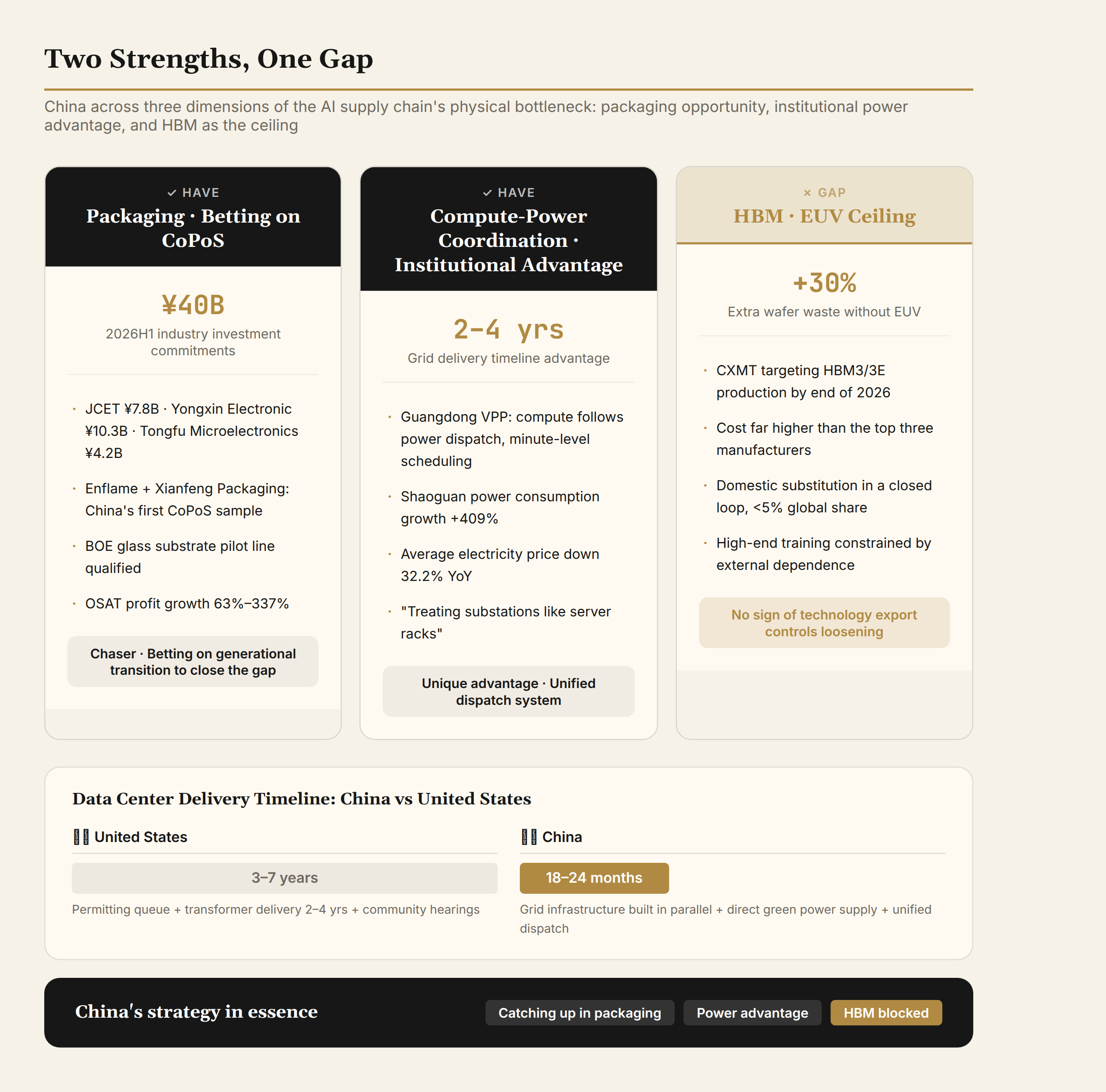
Putting the three dimensions together, China's strategy is a systemic bet: the physical bottleneck period is long enough for the second tier to catch up.
On the packaging side, the bet is on the CoPoS paradigm shift—capturing mid-range orders within 4–5 years. On the power side, institutional differences buy a 2–4 year delivery time advantage. HBM is the one knot that cannot be untied—EUV restrictions show no signs of loosening, and CXMT's HBM can only circulate within a closed domestic substitution loop.
"Two strengths, one gap." Strength in packaging capability (catching up), strength in power dispatch advantage (institutional dividend), gap in HBM self-sufficiency (technology restrictions). This picture is meaningfully better than a year ago, but the HBM weakness may cap the ceiling—without self-sufficient HBM, China's AI chips can only run inference; high-end training remains at the mercy of others.
V. The Thread Behind the Four Walls
Stack the four walls together and the signal is clear.
Capex grows exponentially: $467B → $886.7B → $1.32T. Physical delivery grows linearly: CoWoS capacity doubles but effective output declines, HBM's share of DRAM wafer capacity rises from 23% with LTAs locking 50% of total capacity, grid approval takes 3–7 years, transformer delivery takes 2–4 years, gas turbines are sold out through 2029.
The gap between the two curves is the AI industry's systemic risk. The wider the gap, the greater the bargaining power of bottleneck operators. TSMC's allocation authority over CoWoS capacity, SK Hynix's allocation authority over HBM LTAs, ERCOT's approval authority over grid access—these "gatekeepers" effectively possess the power to decide who can run AI workloads.
The gap is also reshaping the competitive landscape. Google's shift to EMIB, NVIDIA's dual-sourcing, Chinese OSAT order inflow—all are passive adjustments under gap pressure. The cumulative effect: TSMC's CoWoS monopoly is loosening, the HBM Big Three's pricing power is strengthening, and grid infrastructure has become the new scarce resource.
For investors: focus on the upstream of bottleneck segments (CoWoS equipment suppliers, HBM test/bonding equipment, large transformer manufacturers), not downstream integrators. The tighter the bottleneck, the more valuable the upstream.
For China watchers: compute-power coordination is a real advantage, packaging is an opportunity window, and HBM is the ceiling. Over the next two years, China's AI infrastructure build-out speed will significantly exceed that of the U.S., but the chip-layer shortfall will limit how much of this speed advantage converts into a compute advantage.
VI. Three Falsifiable Predictions
Prediction 1: In 2027, at least one top-tier CSP publicly announces a shift of its flagship AI chip to Intel EMIB or a Chinese OSAT solution. The CoWoS supply-demand gap remains at 10–15%; closing the 20% shortfall can only come from alternative suppliers.
Prediction 2: By 2027, HBM long-term agreement coverage reaches 80%+, and an active HBM secondary market emerges (reselling LTA allocations or finished modules). CXMT's HBM3 capacity enters the domestic substitution procurement loop, but global market share remains below 5%.
Prediction 3: By end of 2027, at least one provincial grid in China achieves GW-scale data center load routinely participating in electricity spot market trading. Guangdong or Ningxia are most likely to hit this milestone first, with VPP aggregation scale exceeding 2 million kW.
Data sources: TrendForce (2026-08-03 CSP capex / AI server shipment forecast / 2026-02 HBM share of DRAM wafer capacity at 23%), DigiTimes (2026-07-10 HBM4 price $2→$4-5/Gb / 50% of DRAM capacity locked by LTAs by 2027), Morgan Stanley (2027 CoWoS demand approximately 2.69 million wafers / capacity forecast 200K wafers/month), SemiAnalysis (2026-07 Google Humufish EMIB-T report / 2026-06 CXMT capacity approaching Micron), IEEE ECTC 2026 (Intel EMIB-T: 25 μm bump pitch / 120×120 mm / 9× reticle / 40% lower cost), Bank of America (Rubin GPU 288–384 GB HBM4 / Rubin Ultra V300 576 GB HBM4e), Counterpoint Research (CXMT lacks EUV, needs 30% more wafers), J.P. Morgan (CoWoS supply-demand gap approximately 20%), Ming-Chi Kuo analysis (EMIB-T validation yield approximately 90% vs. 98% for mass production), ERCOT / Texas Governor's Office press release (2026-08-03 474 GW interconnection queue / 90% data centers / comprehensive audit order) / Texas Tribune, CNBC / ERCOT SARA report (Texas peak demand approximately 85 GW), China Southern Power Grid Guangdong Power Grid / CNR (2026-07-22 Guangdong 309 data centers consuming 5.974 billion kWh / Shaoguan +409% / VPP compute-follows-power dispatch), Cailian Press (2026-08-02 virtual power plant AI agents / 2026-07-29 SK Hynix 10-customer LTA), Bloomberg (2026-08-04 Valar Atomics $1B Series B / $6B valuation / Ward 250 criticality) / CNBC (Palantir Q2 $1.94B +93% / Snap Q2), William Blair (GE Vernova gas turbines sold out through 2028) / industry reports (Siemens Energy gas turbines booked through 2029), industry research / IEA report citations (large power transformer delivery 120–200 weeks), EIA capacity data estimates (total U.S. installed generation approximately 1.3 TW), 21st Century Business Herald / Securities Times / Jiemian News (packaging investment: JCET RMB 7.8B / Yongxin RMB 10.3B / TFME RMB 4.22B / industry total approximately RMB 40B), CXMT IPO prospectus and 2026 interim report (Q1 revenue RMB 50.8B +719% / net profit RMB 24.762B +1,688% / monthly capacity 350K wafers). This article does not constitute investment advice. Data as of August 4, 2026.