
This article continues the locsic.com AI networking series. Previous installments: "From CLOS to ZCube: Intelligent Computing Cluster Network Topology Evolution", "Routing and Congestion in 100K-GPU Clusters", "Scale-Across: AI Clusters Are Growing Across Cities".
The Triple Exponential of Compute Demand
AI compute demand is a triple exponential curve. Model parameters grow roughly 10× per year (Qwen3-Max exceeds 1T parameters; ERNIE 5.0 reaches 2.4T). Cluster sizes jump from ten thousand to a hundred thousand GPUs (xAI Colossus: 230K GPUs; Colossus 2 phase one: 550K GB200/GB300; OpenAI's planned 10GW data center equates to 4-5 million chips). Per-GPU compute doubles every generation (NVIDIA Rubin GPU: 50 PFLOPS FP4).
Stack these three curves together and the conclusion is clear: a single GPU cannot hold the model, so you must parallelize. Parallelism requires communication. Communication is becoming the bottleneck.
This article dismantles one core question: when GPU counts scale from 8 to 72, 1024, 8192, what network connects them? Why does NVIDIA's NVLink dominate while every other vendor starts from scratch? The answer lies not in bandwidth numbers but in a more fundamental choice: communication semantics.
Chapter 1: Why GPUs Need Interconnects
The Model Doesn't Fit
An H100 GPU has 80GB of HBM3 memory. A 1-trillion-parameter model in bf16 requires roughly 2TB just for weights. Add gradients, optimizer states, and activations, and the real footprint multiplies. You need 25 H100s just to hold the weights. That's before accounting for KV Cache, context windows, and batch size.
The solution is parallelism: slice the model across multiple GPUs that compute simultaneously. Four primary strategies each impose distinct communication requirements.
Four Parallel Strategies and Their Communication Patterns
Data Parallelism (DP): Each GPU holds the full model and processes different data. After each training step, AllReduce synchronizes gradients. All GPUs aggregate their local gradients into a global gradient, then redistribute it. The communication volume is large but latency-insensitive (gradients are batch-aggregated), making it suitable for cross-node Ethernet or InfiniBand.
Tensor Parallelism (TP): Each weight matrix is sliced across GPUs. Forward pass requires two AllReduce calls per layer (one after the attention output projection, one after the MLP down-projection). Backward pass adds two more. A 100-layer model means 400 AllReduce calls per training step.
The critical detail: each individual communication is tiny. For batch size = 1, hidden size = 8192 in bf16, one AllReduce transfers only 16KB. But with hundreds of calls per step, total time is dominated by per-call fixed overhead. The bottleneck is latency, not bandwidth. This is why tensor parallelism is acutely sensitive to network latency.
Pipeline Parallelism (PP): The model is split by layers, and GPUs process sequentially. Communication volume is small (only activations are passed), but pipeline bubbles introduce overhead. PP communication is point-to-point: bandwidth matters, latency tolerance is high.
Expert Parallelism (EP/MoE): Mixture-of-Experts distributes different experts across GPUs. Tokens must be routed to the correct expert, processed, and gathered back. This is all-to-all communication. Every GPU sends to and receives from every other GPU, in a pattern resembling matrix transposition.
MoE is the fastest-growing source of communication demand. Huawei disclosed three major challenges in training near-trillion-parameter MoE systems: all-to-all communication bottlenecks (large-scale token routing consumes massive bandwidth while compute resources sit idle waiting), uneven load distribution (expert activation frequencies are unbalanced), and excessive operator scheduling overhead (dynamic routing introduces massive numbers of small-grain operations). All three point in the same direction: interconnect bandwidth and latency.
The Communication Wall
The gap between compute capability and communication capability keeps widening. An H100 GPU (SXM) delivers 989 TFLOPS FP16 with 3.35 TB/s memory bandwidth. PCIe 5.0 x16 provides only 128 GB/s bidirectional. The ratio: 26×. And it grows every year.
PCIe's topology constraint makes things worse. The tree structure means GPU-to-GPU communication must transit CPU and system memory. An 8-GPU AllReduce sends data through GPU → Host Memory → PCIe Switch → Host Memory → GPU, multiplying latency 3-5×.
In the 8-GPU server era, this problem was manageable: NVLink provided full-mesh interconnect among 8 cards. But when models require 72, 144, or even 8192 GPUs working in concert, PCIe and the single-node 8-GPU architecture are fundamentally inadequate.
A new interconnect is needed. Latency must drop by 1-2 orders of magnitude (microseconds to hundreds of nanoseconds). Bandwidth must increase 10× or more. And it must support hundreds of GPUs collaborating as one.
That is the problem Scale-Up networking solves.
Chapter 2: What Problems Does the Scale-Up Plane Face
The Scale-Up goal sounds simple: connect dozens to thousands of GPUs into a logical unit that behaves like one giant GPU. But the moment you try, you hit seven walls.
Wall 1: The N² Connection Explosion
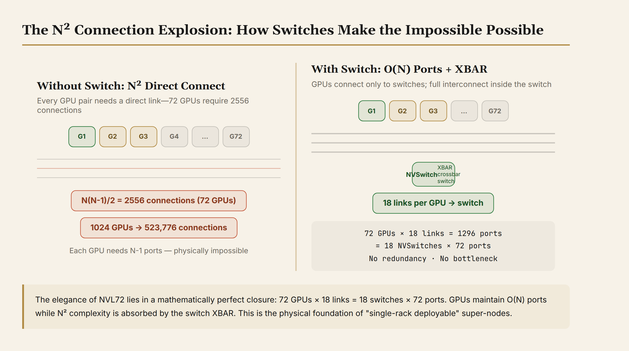
Full-mesh interconnect of N GPUs requires N×(N-1)/2 links. 72 GPUs = 2,556 pairs. 1024 GPUs = 523,776 pairs. GPUs cannot physically wire this many connections. Each GPU has a finite number of pins and SerDes lanes (currently 18-36 NVLink links).
The direction of the solution is switches. GPUs connect only to the switch (O(N) ports), and the switch internally uses a crossbar (XBAR) to achieve any-to-any. But this means the switch absorbs N² complexity, placing enormous pressure on chip design, power, and cost.
Wall 2: The Bandwidth Wall
GPU compute grows far faster than interconnect bandwidth. PCIe 5.0 x16 = 128 GB/s versus H100 memory bandwidth of 3.35 TB/s: a 26× gap. Even NVLink 5 at 1.8 TB/s is only half of memory bandwidth. When TP requires inter-GPU communication approaching memory-read volumes, insufficient interconnect bandwidth translates directly into compute stall.
Wall 3: Synchronization Latency
AllReduce completion time is dictated by the slowest hop. 72 GPUs synchronously waiting for a token round-trip means communication latency becomes compute stall. TP involves hundreds of AllReduce calls per step, each carrying 16KB. The bottleneck is entirely latency. If each call adds microsecond-level overhead, hundreds of calls stack into milliseconds, devastating for inference latency.
Wall 4: Small-Message Efficiency
Memory access granularity is a cache line (64B), but an Ethernet frame header alone is 46 bytes. A 64B payload with a 46B header is 59% overhead. TP's 16KB AllReduce, decomposed into smaller cache-line accesses, forces each one to carry a heavy header burden.
Wall 5: Coherence
When multiple GPUs share an address space, they need to know "is the value I'm reading the latest?" In the CPU multicore world, the MESI protocol solves this. In the cross-chip GPU world, it is an entirely new problem. Hardware cache coherence is extremely complex; software synchronization adds latency.
Wall 6: The Failure Domain
Turning 72 to 8192 GPUs into a logical single machine expands the failure domain from one card to the entire domain. The blast radius of a single-point failure grows dramatically. Meta experienced 419 interruptions during Llama 3 training on 16,000 GPUs. Under a super-node architecture, a single NVSwitch failure can affect 72 GPUs.
Wall 7: Power and Cooling
NVL72 consumes 120-140kW per rack. Liquid cooling is mandatory. The per-bit power of SerDes directly determines TCO. At 224G PAM4 rates, copper cable transmission distance compresses to under 1 meter, making optical interconnect (CPO/NPO) a necessity.
These seven walls are not independent. They couple tightly: the bandwidth wall forces more links (Wall 2), which worsens N² (Wall 1), and switches add hops that make latency harder to control (Wall 3). Scale-Up design is the art of balancing these constraints.
Chapter 3: The Solution Space
Memory Semantics
Why Message Passing Falls Short
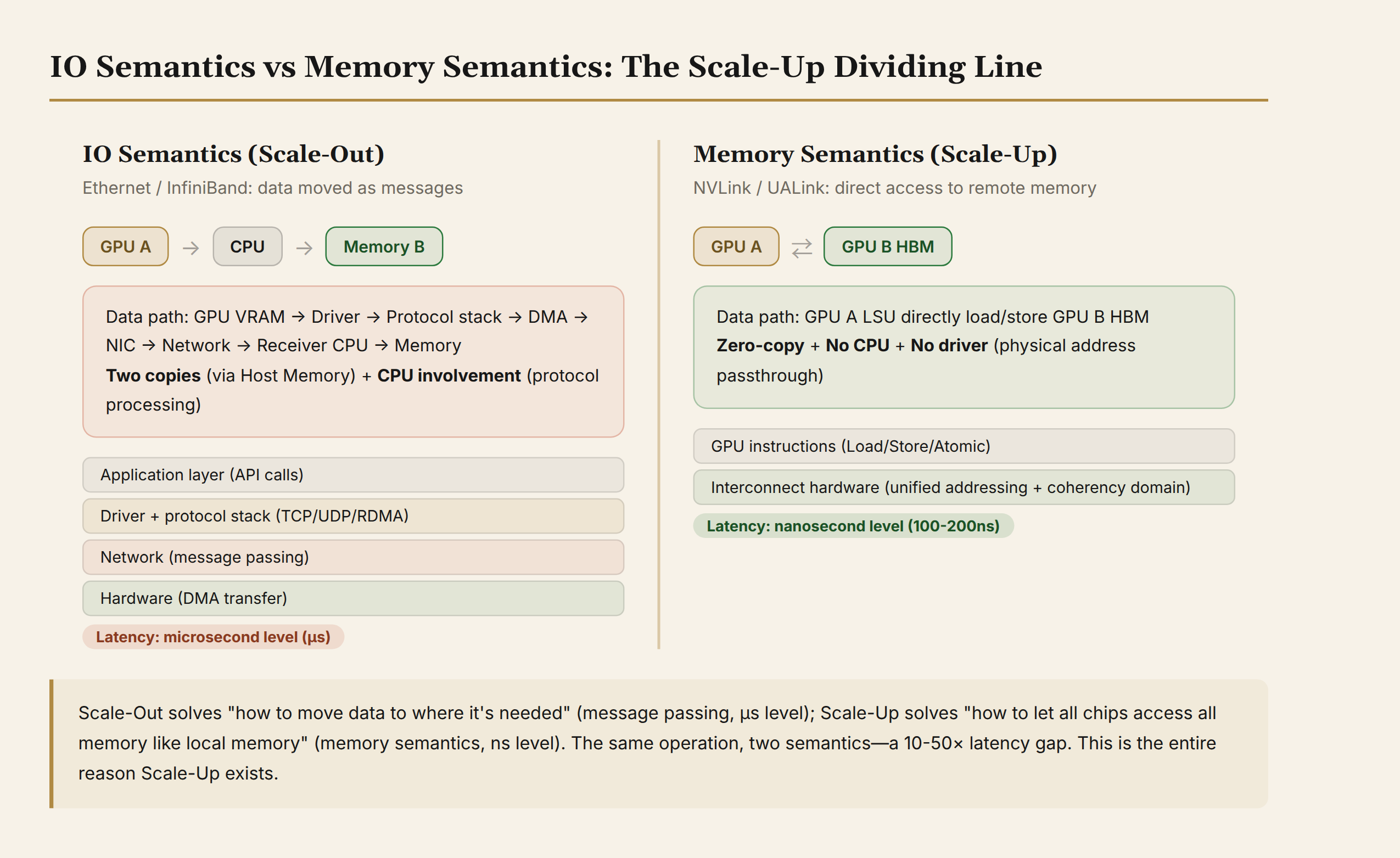
Among the seven walls in Chapter 2, Wall 3 (latency) and Wall 4 (small-message efficiency) point to the same root cause: the IO semantics of traditional networks (message passing) impose excessive overhead in fine-grained, high-frequency scenarios.
In the IO-semantics world, data moves in messages. For a GPU to read remote memory, it must: construct a DMA descriptor → hand it to the driver → traverse the protocol stack → NIC transmits → receiving-side CPU processes → write to memory. Latency: microseconds. And the CPU must intervene.
Under TP, one step means 400 AllReduce calls, each 16KB. If every call goes through IO semantics, overhead stacks into milliseconds. Inference TPOT (time per output token) increases by orders of magnitude.
Memory semantics is the alternative path. The GPU directly issues Load/Store instructions to access remote memory, exactly as it would access local DRAM. No DMA, no driver, no CPU involvement. Latency drops to nanoseconds.
This is the fundamental dividing line between Scale-Up and Scale-Out. Scale-Out (Ethernet/InfiniBand) solves "how to move data to where it's needed": message passing, microseconds. Scale-Up (NVLink/UALink) solves "how to let every chip access all memory as if it were local": memory semantics, hundreds of nanoseconds.
Five Pillars
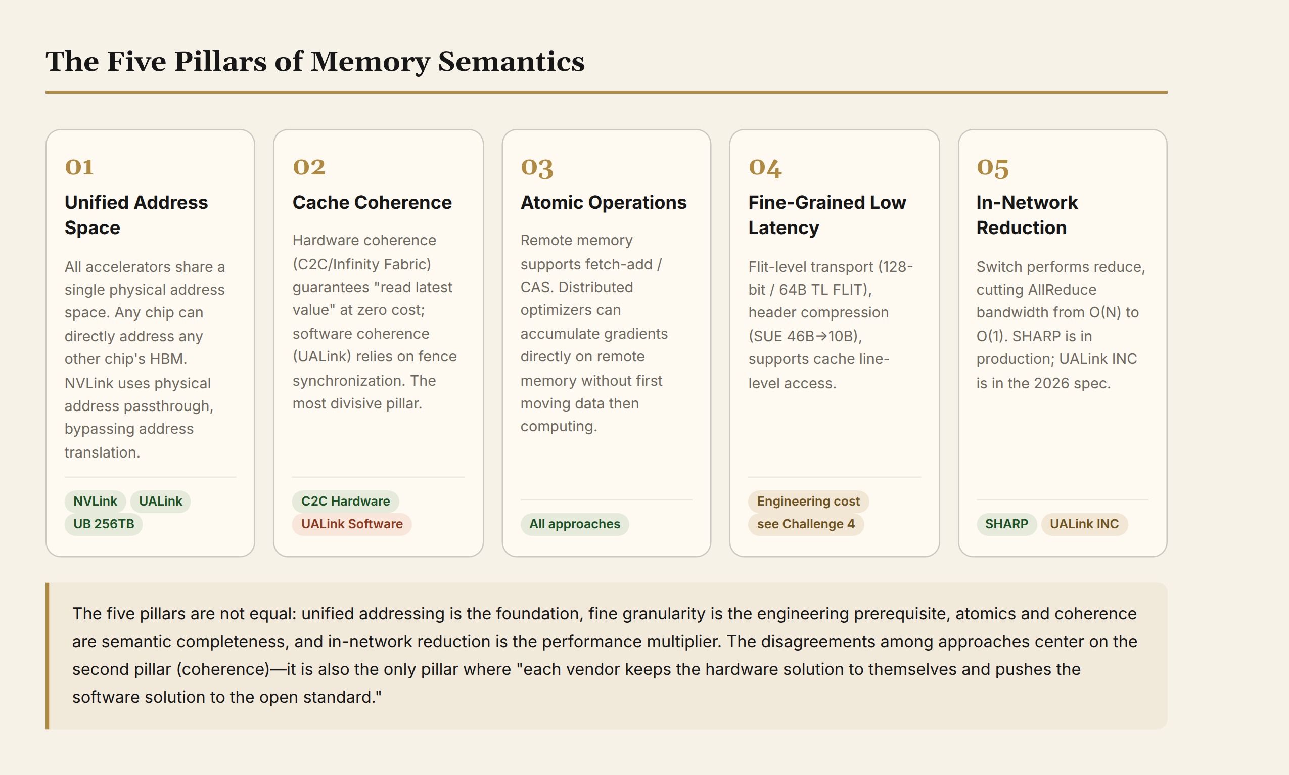
Memory semantics is not a single technology. It is the combination of five pillars.
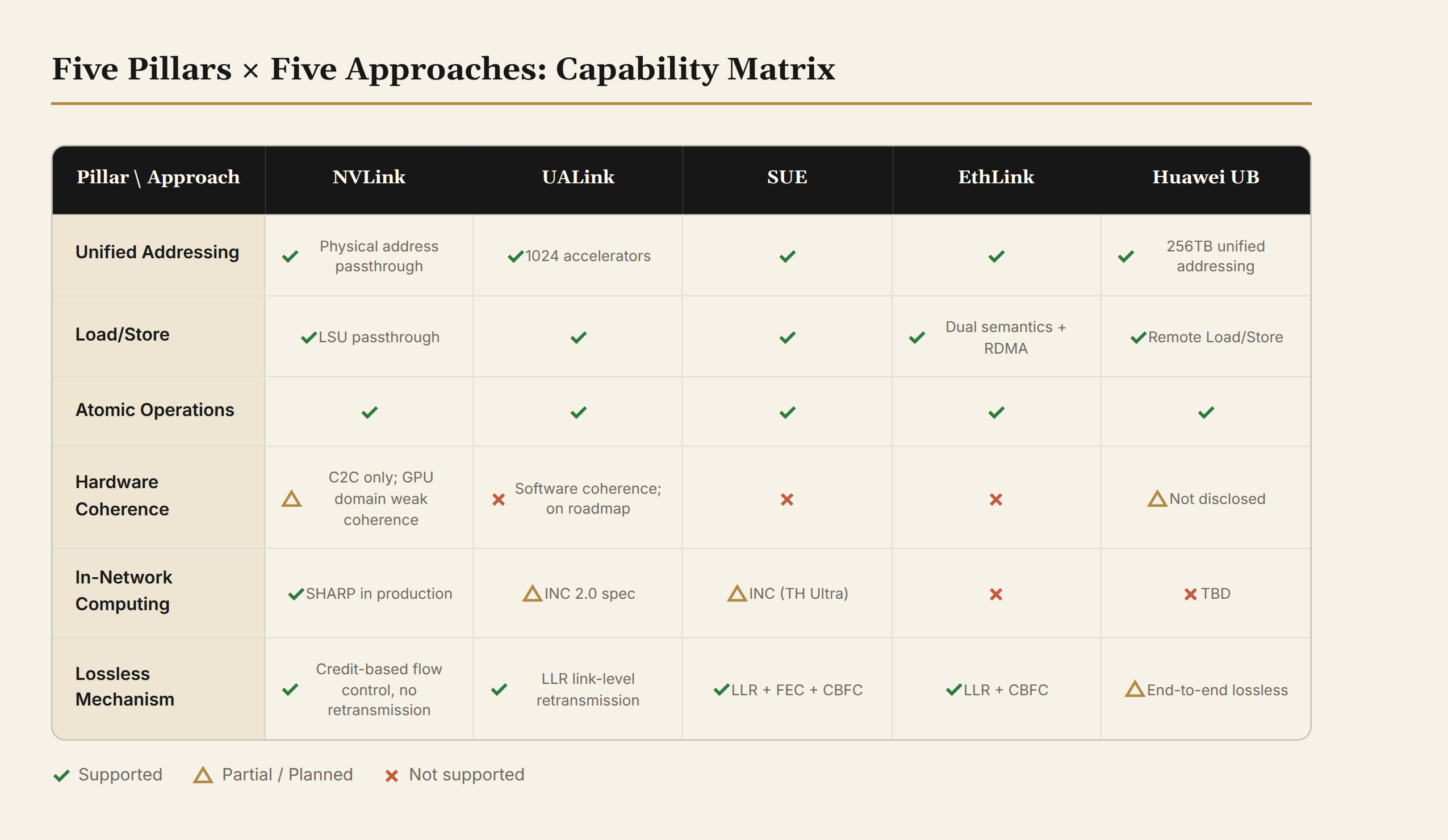
Pillar 1: Unified Address Space. All accelerators share a physical address space. Any chip can directly address any other chip's HBM. NVLink uses physical-address pass-through, bypassing virtual address translation. Huawei Lingqu UB provides a 256TB global unified memory address space. Without unified addressing, there is no Load/Store pass-through.
Pillar 2: Cache Coherence. Unified addressing solves "can I find the remote memory?" Coherence solves "is what I read the latest?" This is the pillar with the most divergence.
Hardware cache coherence (extending CPU-style MESI protocols across chips) guarantees software needs no manual synchronization. NVLink-C2C's SCF architecture and AMD Infinity Fabric implement this. Software coherence relies on explicit synchronization (fence, atomic), adding latency but simplifying implementation. UALink chose this.
The key judgment: every vendor keeps hardware coherence within its own ecosystem (NVIDIA C2C / AMD Infinity Fabric) and pushes software coherence to the open standard (UALink). Coherence protocols are core microarchitectural IP. Opening them is equivalent to opening chip design. This is not a technical compromise; it is business logic.
Pillar 3: Atomic Operations. Remote memory supports atomic instructions (fetch-add, CAS). Distributed optimizer gradient aggregation can atomically accumulate directly on remote memory without first moving data and then computing. NVSHMEM provides floating-point atomic add/fetch_add APIs.
Pillar 4: Fine-Grained Low-Latency Access. Flit-level transmission. NVLink uses 128-bit Flits (25b CRC + 83b transaction layer + 20b link layer). One header + 16 payload = 256B, peak efficiency 94.12%. UALink uses 64B TL FLITs packed into 640B DL FLITs. SUE compresses the Ethernet header from 46B to 10B. The engineering cost of fine-grained access (header compression, small-packet efficiency) is a central theme of Chapter 5.
Pillar 5: In-Network Reduction. Reduce inside the switch. AllReduce communication complexity drops from O(N) to O(1). Without in-network reduction, 72 GPUs doing AllReduce need 72 copies of data fully interconnected. With it, each port transmits only the reduced result. NVIDIA SHARP performs reduction inside NVSwitch. UALink 2.0's In-Network Compute provides ReadReduce/WriteMulticast/Broadcast/Reduce/AllReduce primitives.
The Latency Cliff
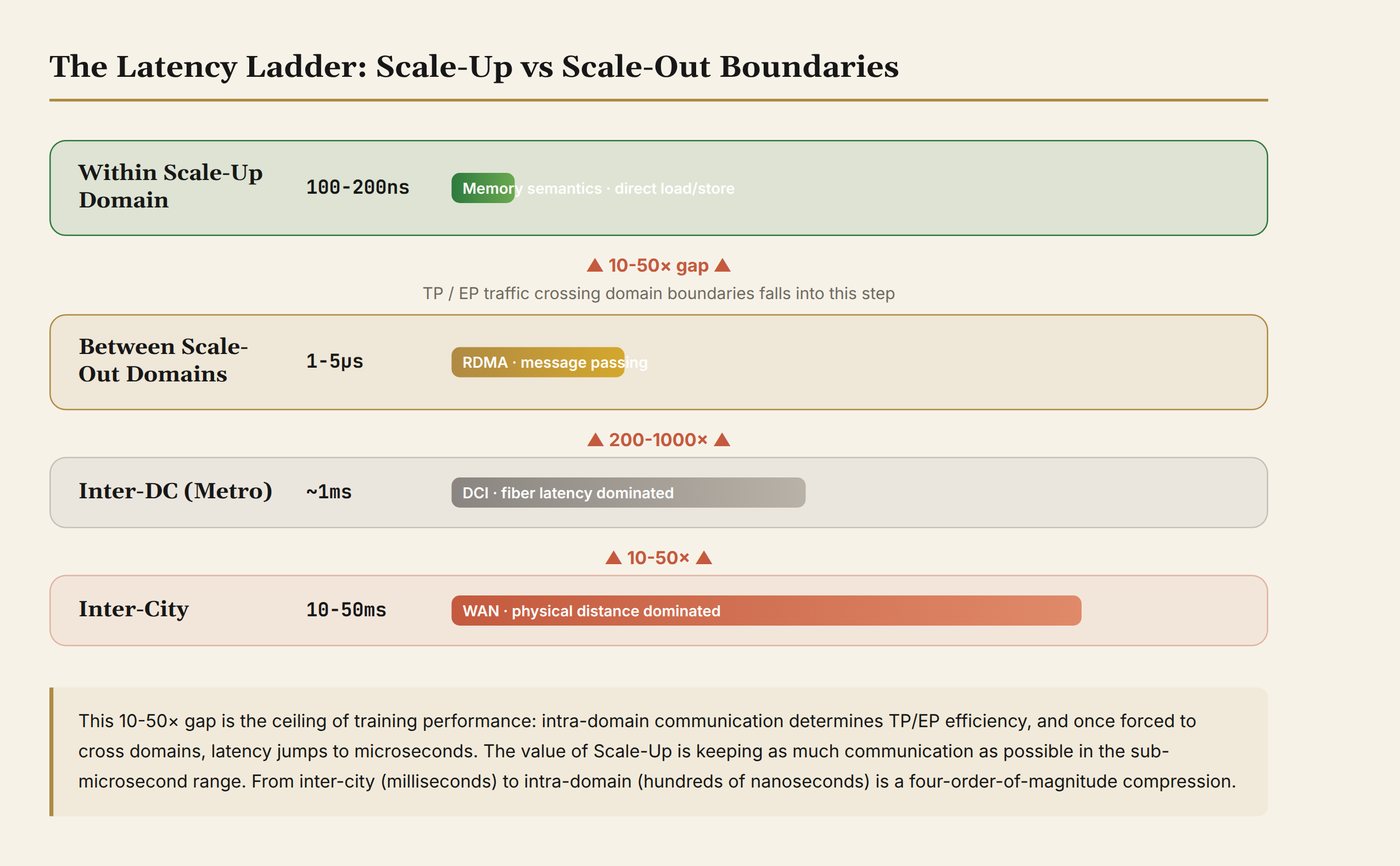
The cost of memory semantics is that it pulls interconnect to a new latency threshold:
| Tier | Latency | Semantics |
|---|---|---|
| Within Scale-Up domain | 100-200ns | Memory semantics (Load/Store pass-through) |
| Across Scale-Out domain | 1-5µs | RDMA (message passing) |
| Intra-city | 1ms | Network |
| Inter-city | 10-50ms | Network |
Between intra-domain hundreds-of-nanoseconds and cross-domain microseconds lies a steep 5-50× cliff. If TP/EP communication is forced across domains, it falls into microsecond territory and back into the congestion and routing problems discussed in the previous article. The entire purpose of Scale-Up is to keep as much communication as possible in the hundred-nanosecond regime.
The solution space is now defined. The next question: who does what, and why.
Chapter 4: NVIDIA's Choices, How NVLink Answers Every Question
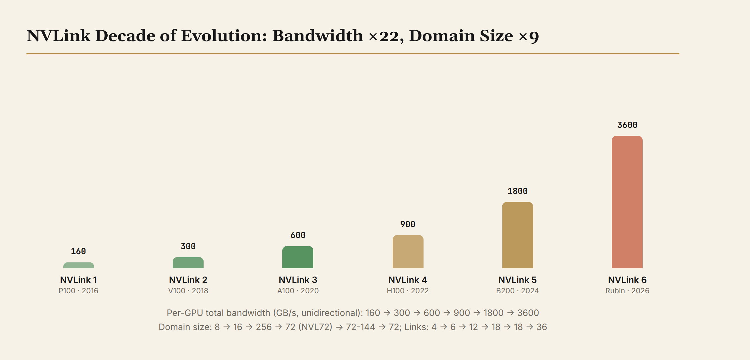
NVIDIA spent a decade answering the seven walls of Chapter 2. Each wall corresponds to a technical decision, each with a clear rationale and cost.
Bandwidth: Multi-Link Aggregation + Per-Generation Doubling
NVLink progressed from 160 GB/s in 2016 (4 links) to 3.6 TB/s in 2026 (36 links). Twenty-two-fold growth over a decade. Each link evolved from 20G NRZ to 224G PAM4, with per-generation rate doubling.
| Generation | Per-Link Bidirectional | Per-GPU Total Bandwidth | Domain Size | Representative |
|---|---|---|---|---|
| NVLink 1 | 40 GB/s | 160 GB/s (4 links) | 8 GPU | P100 |
| NVLink 2 | 50 GB/s | 300 GB/s (6 links) | 16 GPU (NVSwitch) | V100 |
| NVLink 3 | 100 GB/s | 600 GB/s (12 links) | 256 GPU | A100 |
| NVLink 4 | 100 GB/s | 900 GB/s (18 links) | 72 GPU (NVL72) | H100 |
| NVLink 5 | 200 GB/s | 1.8 TB/s (18 links) | 72-144 GPU | B200 |
| NVLink 6 | 200 GB/s | 3.6 TB/s (36 links) | 72 GPU | Rubin |
Note: NVLink generations 1-3 bandwidth figures are bidirectional (NVIDIA's early marketing convention). From NVLink 4 onward, the unidirectional convention is used.
N² Connections: NVSwitch Crossbar
72-GPU full-mesh interconnect requires 2,556 pairs. NVIDIA's answer: NVSwitch. GPUs don't connect directly; they go through switches for full-mesh. Each GPU connects 18 NVLink links to the switch, and the switch's internal XBAR (crossbar) enables any-to-any.
NVL72 math: 72 GPUs × 18 links = 1,296 ports = 18 NVSwitch chips (72 ports each) × 72 ports. No redundancy, no bottleneck: 72 ports match 72 GPUs. Physical implementation: 18 compute trays + 9 switch trays + 5,000 coaxial copper cables, all in one rack.
Every constraint in this math comes from physical reality: each NVSwitch chip has exactly 72 ports, each GPU has exactly 18 NVLink links. 72 is not the theoretical optimum. It is the engineering optimum for single-rack deliverability.
Tail Latency: Removing All Uncertainty
NVLink made an aggressive choice: removing end-to-end retry and adaptive routing. Both are standard features in Ethernet/InfiniBand. In NVLink, they are enemies because they introduce unpredictable latency.
Memory semantics demands that "a Load instruction returns within a predictable time." If a retransmission causes one Flit's latency to double, the entire pipeline stalls. Removing uncertainty buys 100-200ns of predictable latency.
Physical-address pass-through extends the same philosophy: no virtual address translation. The GPU's LSU directly accesses remote HBM using physical addresses. Every layer strips away unpredictability.
Small Messages: Flit + SHARP In-Network Reduction
The 128-bit Flit format minimizes header overhead (94.12% payload efficiency). More critically, SHARP: every NVLink switch has a built-in SHARP engine. AllReduce is completed inside the switch, requiring no GPU compute for communication reduction.
Under TP, this means all 400 AllReduce calls per step are digested by switch hardware. GPU compute is 100% devoted to computation. NCCL automatically detects and enables SHARP. A decade of software stack investment pays off here: topology awareness, PXN routing optimization, SHARP utilization, production hardening.
Coherence: Scenario Differentiation
NVIDIA's choice: weak coherence with software fence/atomic synchronization for the GPU-to-GPU domain, hardware coherence for CPU-GPU (NVLink-C2C's SCF architecture).
Why no hardware coherence for the GPU domain? Because AI workload access patterns are batched, regular, and predictable. AllReduce, MoE routing, weight broadcast: NCCL's streaming plus fence is sufficient. CPU-GPU coordination involves unpredictable pointer chasing and sparse access, where hardware coherence is needed to guarantee "what you read is always the latest."
NVLink-C2C is a separate design: single-ended parallel signaling (9 data + 1 clock, like DDR rather than high-speed serial), extending die-to-die interconnect beyond the package. Power: 1.3 pJ/bit, one-fifth of PCIe. The Grace Hopper superchip uses C2C to connect CPU and GPU with coherent shared memory, requiring no manual software synchronization.
Failure Domain: Hot-Swap and Graceful Degradation
NVLink 6 switches introduced three availability features: control-plane high reliability (control-plane faults don't interrupt the data plane), partial-rack operation (degraded mode when some GPUs fail), and switch-tray hot-swap (>500 insertion cycles). If one of 72 NVSwitches fails, only the affected GPUs lose partial links. Training slows but doesn't stop.
Power: C2C Per-Bit Efficiency
NVLink-C2C's 1.3 pJ/bit is the lowest among all approaches (an inherent advantage of single-ended parallel signaling). But NVL72's 120-140kW per-rack power still requires liquid cooling. The next-generation Feynman platform plans to mount CPO (co-packaged optics) chips directly on switch trays, solving copper cable distance limitations at 224G+ rates with optical interconnect.
The Cost: Lock-In
NVIDIA's solution comes at a cost: lock-in. NVLink is a proprietary protocol. NVSwitch is a proprietary chip. NVSHMEM and NCCL are deeply bound to NVIDIA hardware. Maximum performance, deepest vendor lock-in.
NVLink Fusion attempts to mitigate this by licensing third-party chips to integrate NVLink IP. But the "semi-open" reality: the hardware protocol layer is open (PHY, link, transport, coherence, atomic), while the software layer remains controlled (link bring-up, NVSwitch licensing, platform must include at least one NVIDIA product). Customers using third-party NVLink designs need NVIDIA approval.
Chapter 5: Starting Points of the Open Camp
Common Premise: The NVIDIA Tax
Every open route starts from the same premise: not wanting to be locked into NVIDIA.
NVIDIA holds roughly 80-95% of the AI accelerator market. Customers face: steep premiums (GPU + NVSwitch + InfiniBand + software licensing, all charged as a full stack), delivery lead times stretching beyond half a year, and feature upgrades held hostage to a single vendor's roadmap.
But breaking a monopoly requires more than willingness. It requires a technical alternative. Scale-Up interconnect is the core component of that alternative. If you can define an open high-speed interconnect protocol that lets any vendor's GPU or accelerator plug in and work, you shake NVIDIA's infrastructure lock-in.
AMD: From Substitute to Challenger
AMD long held the role of AI accelerator substitute. Customers only considered AMD when NVIDIA couldn't deliver. In July 2026, AMD signed a multi-tens-of-billions-dollar partnership with Anthropic: Anthropic will procure up to 2GW of AMD Instinct MI450 chips, with deliveries starting in the first half of 2027, and AMD will invest up to $5 billion in Anthropic. This marks AMD's first direct investment in an AI company.
The deal's significance extends beyond procurement. Anthropic is systematically building a compute supply chain independent of NVIDIA. AMD must prove MI450 can handle training, not just inference. That is the hardest barrier in the AI chip market.
AMD's Scale-Up weapon is Infinity Fabric. Five generations of evolution, from inter-core CPU connectivity to cross-node, cross-rack unified scheduling of CPU/GPU/accelerators. Inside MI455X, two FCDs (cache and interconnect dies) connect through a central Infinity Fabric, coordinating cache coherence and providing system-level atomic operations.
But AMD did not make Infinity Fabric into another closed standard. Instead, it drove the formation of the UALink Consortium.
UALink: The Open United Front
The UALink Consortium was founded by 9 inaugural board members: AMD, Astera Labs, AWS, Cisco, Google, HPE, Intel, Meta, and Microsoft. Alibaba Cloud, Apple, and Synopsys later joined the board. Membership exceeds 100 companies, including ByteDance, Tencent, ZTE, H3C, and ARM.
UALink 1.0 defines a complete four-layer protocol stack: UPLI (protocol layer interface, providing the memory-semantic bus interface), TL (transaction layer, 64B TL FLITs + credit-based flow control), DL (data layer, 640B DL FLITs + LLR link-layer retransmission), PL (physical layer, based on Ethernet 802.3dj). Per-channel: 200 Gbps. Per-port maximum: 800G. Supports 1,024 accelerators. UALinkSec hardware encryption + TEE (SEV/TDX).
UALink 2.0 (released April 2026) adds four specifications: Common 2.0 adds In-Network Compute (ReadReduce/WriteMulticast/Broadcast/Reduce/AllReduce), DL/PL 2.0 splits independently and adds link resiliency and link folding, Manageability 1.0 introduces centralized management (gNMI/YANG/SAI/Redfish), and Chiplet 1.0 is compatible with UCIe 3.0.
The UALink roadmap explicitly lists hardware memory coherence as a future-version feature. Versions 1.0 and 2.0 are software-coherent.
AMD's dual-track strategy is now clear: its own Infinity Fabric provides hardware cache coherence (competitive advantage for selling MI-series chips), while the UALink specification provides software coherence (the cross-vendor open compromise). This mirrors NVIDIA: both keep hardware coherence within their own ecosystem (C2C / Infinity Fabric) and push software coherence to the open standard (NVSwitch-domain weak coherence / UALink).
Broadcom: The Logic of Selling Switch Chips
Broadcom doesn't make GPUs. It makes switch chips. Its Scale-Up solution is SUE (Scale-Up Ethernet), adopted by OCP's ESUN working group as the recommended transport protocol.
SUE's strategy differs from UALink: it uses only the Ethernet physical layer, with everything above entirely different from traditional Ethernet. Two-and-a-half layers. No TCP/IP/UDP. Point-to-point connections, borrowing NVLink transport logic. The name says Ethernet, but it behaves more like a proprietary bus protocol running on Ethernet PHY.
The hardware foundation is Tomahawk Ultra: 51.2 Tbps aggregate bandwidth, full-speed throughput even with 64B small packets, latency under 250ns. Headers compressed from 46B to 10B (78% reduction). LLR + FEC link-layer retransmission, CBFC credit-based flow control, INC in-network collective computation.
Broadcom's logic for switch chips: maximize the reuse surface of the Ethernet ecosystem. SUE reuses standard Ethernet SerDes, MAC, switch ASICs, and operational toolchains, but strips the protocol stack to its thinnest form. Customers don't need to learn an entirely new protocol to gain Scale-Up capability. Companies building UALink switches mostly come from PCIe Switch backgrounds. This is not a coincidence.
ByteDance: Dual Semantics Optimized for Internal Use
ByteDance's 2026 capital expenditure was originally set at 160 billion RMB (later raised to approximately 200 billion), of which roughly 85 billion goes directly to AI chip procurement. Training and inference chip supply chains are now fully separated: large-scale training uses Huawei Ascend and Cambricon; online inference introduces Iluvatar CoreX and other specialized inference GPUs.
ByteDance's Scale-Up solution is EthLink, co-designed with Peking University and based on Ethernet. Its distinguishing feature: dual semantics, simultaneously supporting Load/Store and RDMA.
Upper-layer applications choose flexibly by scenario: latency-sensitive TP synchronization uses Load/Store (the GPU's LSU directly issues Memory Read/Write), while bandwidth-sensitive bulk data transfer uses RDMA (SM initiates, RDMA Engine executes). The protocol stack splits into two layers: the Scale-Up semantic layer (GPU operations + transaction layer, defining Memory Read/Write/Atomic/Message) and the Scale-Up network layer (LLR + CBFC + compressed headers).
ByteDance's insight: not all traffic needs memory semantics. Coexisting dual semantics, letting the programming model choose by load characteristic, is EthLink's differentiated contribution to UALink and SUE. ByteDance later joined the UALink Consortium, and some EthLink ideas have been absorbed.
Huawei: Full-Stack Self-Reliance
Huawei's situation differs from every other vendor. It simultaneously faces technology sanctions and supply chain restrictions. Self-reliance is not a strategic preference but an existential necessity.
Huawei's Scale-Up solution is Lingqu (UnifiedBus / UB), fully self-developed. The physical layer supports two modes: Mode-1 uses custom rates (can drive 160G without being constrained by standard 112G/224G limits), and Mode-2 is compatible with standard Ethernet electrical specifications. The protocol stack from physical layer to functional layer is entirely self-developed, combining existing technologies including Ethernet, link aggregation, IPv4/IPv6, MCTP, SPDM, and SM4 encryption.
The Ascend 950 super-node (Atlas 950 SuperPoD) was publicly demonstrated at WAIC 2026: 1,024 cards (scalable to 8,192 for the full Atlas SuperPoD), 256TB global unified memory addressing, 3µs RTT, 2TB/s interconnect bandwidth. The Atlas 950 SuperCluster scales to 500,000 cards.
Huawei has commercially deployed over 750 Ascend 384 super-node systems, covering internet, telecom, finance, and education sectors. The CANN heterogeneous computing architecture is fully open-sourced with over 12.44 million lines of code and 3,500+ monthly active developers (Huawei official data). Liang Wenfeng (DeepSeek founder) publicly stated: Huawei's 950 super-node can functionally replace the GB200 NVL72, with equivalent task-level and latency performance, at the cost of needing 4 Huawei cards for roughly the compute of 1 NVIDIA card, with chip iteration cadence trailing by about two years.
Chapter 6: Why Multiple Approaches Emerged
Chapter 5 showed five vendors making different choices. But the real question: why no unified standard?
Divergence 1: Physical Layer
NVIDIA chose proprietary PAM4 SerDes (from 20G to 224G+). Every other vendor chose Ethernet PHY. This is not a technical preference. It is an ecological niche difference. NVIDIA needs extreme performance to justify its closed-ecosystem premium. Other vendors need to reuse the Ethernet supply chain to lower cost and entry barriers.
Ethernet's Moore's law (per-chip bandwidth doubling every 18 months), mature SerDes/optical module/connector supply chains, and globally deployed operational toolchains form a gravitational pull that proprietary approaches cannot resist. UALink's latest physical layer has switched from PCIe to Ethernet. SUE, EthLink, ETH-X, and ETH+ are all Ethernet-based.
Divergence 2: Coherence
Hardware coherence provides zero-cost synchronization guarantees, but exists only in NVIDIA C2C and AMD Infinity Fabric. UALink 1.0/2.0 chose software coherence, with the roadmap planning to add hardware coherence in future versions.
Why doesn't UALink do hardware coherence? Because cross-vendor hardware coherence requires a unified coherence protocol, and AMD/Broadcom/Intel/Google chips have fundamentally different cache models. Coherence protocols are core microarchitectural IP. Opening them is equivalent to exposing chip design details. Keeping hardware coherence for oneself and pushing software coherence to the open standard is the shared business logic of NVIDIA and AMD.
Divergence 3: Protocol Stack Thickness
UALink's four layers are the most complete (UPLI/TL/DL/PL), because cross-vendor compatibility requires standardizing every layer's interface so that different chips' cache models and transaction semantics interoperate within a unified framework. SUE's two-and-a-half layers are the thinnest, because it targets only one switch chip (Tomahawk Ultra). No cross-vendor need means it can strip the stack to absolute minimum. EthLink's dual semantics are the most flexible, choosing Load/Store or RDMA as needed. Huawei UB is full-stack self-developed, because it depends on no external standard.
Thickness determines the balance between compatibility and performance. Thicker stack: better cross-vendor compatibility, more latency overhead. Thinner stack: more extreme performance, closer to proprietary. UALink chose compatibility. SUE chose performance. EthLink chose flexibility.
Divergence 4: Lossless Mechanism
NVLink removed end-to-end retry (pursuing deterministic latency). UALink, SUE, and EthLink retain LLR link-layer retransmission because they reuse Ethernet PHY, whose physical-layer reliability is lower than proprietary designs. Link-layer retransmission is the necessary backup. This is the cost of the "Ethernet physical layer" route: you enjoy supply-chain maturity, and you accept an extra layer of link-layer retransmission overhead.
Essence: Business Logic Drives Technical Divergence
Behind the four divergences lies one pattern: a chip vendor's commercial position determines its technical choices. NVIDIA relies on vertical integration to sell at a premium. It chooses closed and proprietary. AMD relies on standard-setting alliances to break the monopoly. It chooses open plus dual-track. Broadcom profits from selling switch chips. It chooses the thinnest stack to maximize customer reach. ByteDance optimizes for internal use to reduce cost. It chooses dual semantics. Huawei relies on full-stack self-reliance to survive sanctions. It chooses full-stack self-development.
Technical divergence is not "whose technology is better." It is "whose business model requires what technology."
Chapter 7: Progress and the Architect's Decision
Where Each Player Stands
NVIDIA: NVLink 6 enters mass production with the Rubin platform. Vera Rubin NVL72 is in large-scale manufacturing. NVLink Fusion partners (MediaTek, Marvell, Alchip, Astera Labs, Synopsys, Cadence) hold licenses. Intel and Samsung have joined. But the "semi-open" substance remains unchanged: platforms must include at least one NVIDIA product, and third-party designs require NVIDIA approval. NVLink's closed ecosystem will remain irreplaceable through 2026-2027. Fusion's semi-openness is a defensive posture, not a proactive choice.
UALink: Switches and accelerators compliant with the 1.0 specification are expected to ship late 2026 to early 2027. Marvell demonstrated a 576-lane UALink Switch (under 800W). AMD MI450 GPUs will use UALink interconnect, with 72 lanes per GPU at 200G. Products corresponding to the 2.0 specification are expected late 2027 to early 2028. The 3.0 specification is anticipated in 2027. This means the first non-NVIDIA Scale-Up interconnect clusters will appear in 2027. The open ecosystem moves from specification to product.
Huawei: The Ascend 384 super-node has been commercially deployed in 750+ systems. The Atlas 950 SuperPoD (1,024 cards) is planned for market release in Q4 2026. Sugon's 100,000-card super-cluster is already operational in Zhengzhou. This is one of the largest non-NVIDIA AI compute deployments worldwide, demonstrating that domestic Scale-Up has passed validation and entered large-scale commercial deployment.
ByteDance: EthLink has joined the UALink Consortium. Technical contributions are being absorbed. ByteDance is simultaneously advancing its dual training-inference supply chain (training on Ascend/Cambricon, inference on Iluvatar CoreX and others). China's largest AI compute buyer is systematically reducing dependence on a single supplier.
How to Choose Domain Size
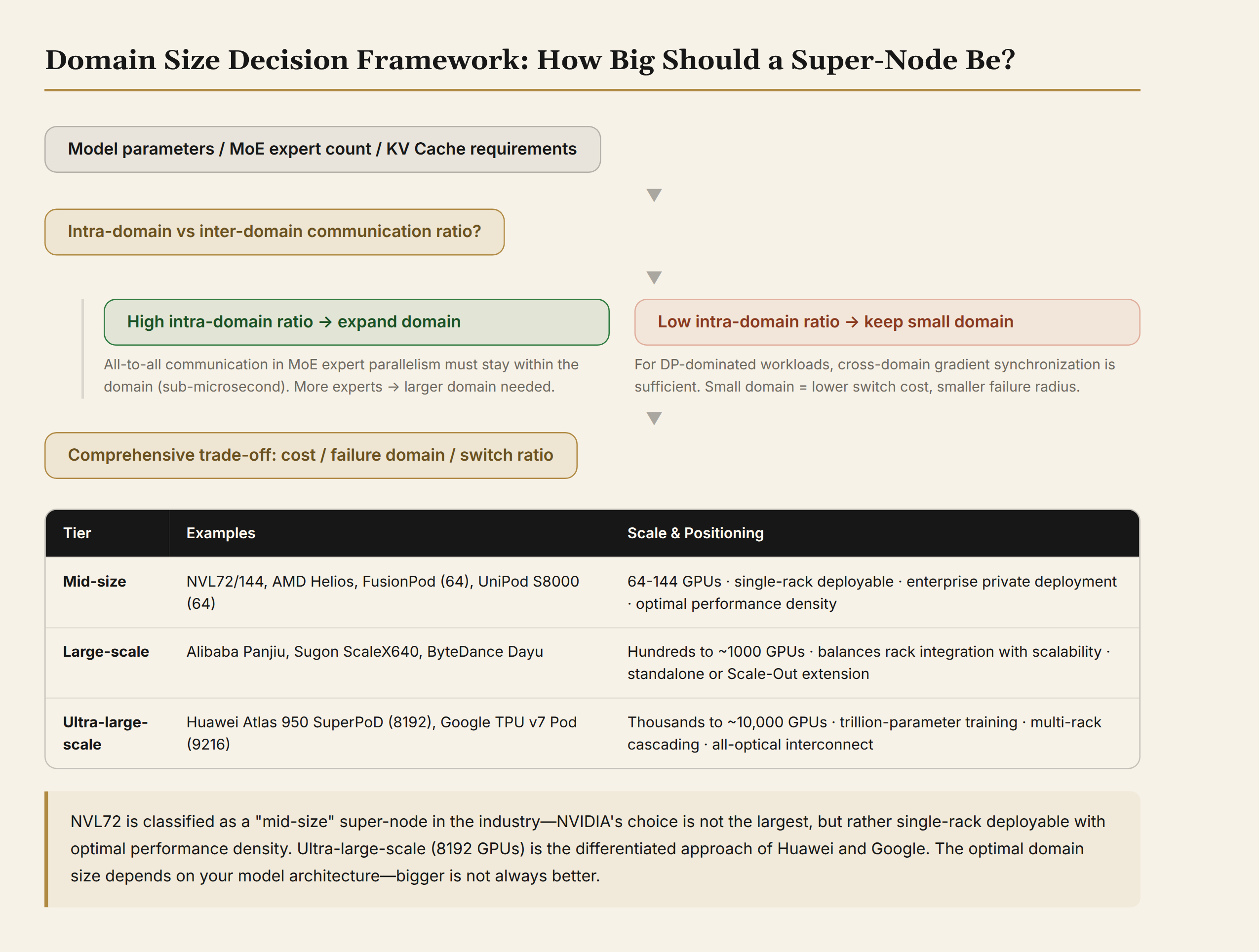
The first decision an architect faces is domain size. Bigger is not better. Too small: TP/EP is forced across domains, communication falls back to microseconds. Too large: switch layers multiply, costs explode (NVL72's switch ratio is 1:2, one switch chip per 2 GPUs), and the failure domain grows.
MoE is the primary driver of domain size. Expert parallelism demands that token-routing all-to-all completes within the domain (hundred-nanosecond level). The number of experts sets the minimum domain size.
The industry has settled on three tiers:
| Tier | Representative Systems | Scale | Positioning |
|---|---|---|---|
| Medium | NVL72/144, AMD Helios 72/144, H3C (64), xFusion (64) | 64-144 cards | Single-rack delivery, optimal performance density |
| Large | Alibaba Panjiu, Sugon ScaleX640, ByteDance Dayu | Hundreds to ~1,000 cards | Balance of integration and scaling |
| Ultra-large | Huawei Atlas 950 SuperPoD (8,192), Google TPU v7 Pod (9,216) | Thousands to ~10,000 cards | Trillion-parameter training |
NVL72 is classified as "medium" in the industry. NVIDIA's choice is not the largest. It is the single-rack-deliverable, performance-density optimal.
TCO Reality
Liang Wenfeng's substitution assessment provides a golden reference point: Huawei's 950 super-node can replace the GB200 NVL72 with equivalent task-level and latency performance, but it costs 4× the cards to match 1× the compute, with chip iteration trailing two years.
The architect's interpretation: system-level capability (super-node interconnect + software stack) has caught up. But the per-chip generational gap persists. Compute-density-sensitive workloads choose NVIDIA. Supply-chain-security or cost-sensitive workloads choose Huawei, paying with 4× the cards and higher power consumption.
Scale-Up's cost center is shifting from optical modules (the Scale-Out era) to switch chips + copper cables/connectors + liquid cooling. Dell predicts that by 2028, Scale-Up port demand will exceed Scale-Out by 2× or more. LightCounting estimates the 2027 Scale-Up switch market at $14 billion.
Assessment
Ethernet physical layer + memory semantics = the greatest common divisor. Every camp outside NVLink builds on Ethernet PHY. This is not coincidence. It is the gravitational pull of Ethernet supply-chain maturity and Moore's law.
Software coherence: how long is "good enough"? AI workloads' "write-once-read-many" access pattern makes software coherence sufficient for now. But two trends may change this judgment within 2-3 years: agentic workloads with fine-grained collaboration, and MoE scaling driving frequent inter-expert reads. When that happens, hardware coherence shifts from a bonus to a requirement.
NVIDIA's moat is not NVLink. It is the full stack. SHARP in-network computation + NVSHMEM programming model + a decade of NCCL optimization. Multiple competitors are catching up at the protocol layer, but ten years of communication library accumulation (topology awareness, PXN routing optimization, SHARP utilization, production hardening) cannot be replicated overnight.
China's dual track is clear: Huawei full-stack self-development (mirroring NVIDIA's vertical integration), and the Ethernet open route joining the UALink Consortium (mirroring AMD's open standards). UALink 1.0 products ship late 2026. Version 3.0 hardware parity arrives 2028+. The open ecosystem trails NVIDIA by more than one generation, but the gap is closing continuously.
Conclusion
Memory semantics is the price of entry. All five camps have paid it. The full stack is what wins. Only NVIDIA has one.
But the entry fee keeps dropping: Ethernet PHY's Moore's law, UALink's open ecosystem, Chinese vendors' pursuit, all lower the barrier. When memory semantics becomes commodity infrastructure, competition shifts from the protocol layer to the application layer. Training frameworks. Programming models. Toolchains.
Whoever turns the data center into a single computer owns the foundation of the AI era. That sentence still belongs to NVIDIA. But the foundation is cracking.
Disclaimer: This article is based on NVIDIA/AMD/Broadcom/Huawei/ByteDance public materials, UALink Consortium specifications, Marvell/ZTE/H3C technical analyses, SGLang technical documentation, industry research reports, and cross-verification with previously published locsic.com AI networking series articles. This article does not constitute investment advice. Data is current as of 2026-07-31.