
AMD Helios Supernode Teardown: Can Ethernet-Based Scale-Up Challenge NVLink's Moat?
On July 23, 2026, AMD unveiled the Helios rack-scale AI platform at Advancing AI 2026. 72 MI455X GPUs, 31TB of HBM4, UALoE (Ultra Accelerator Link over Ethernet) scale-up interconnect, plus a 2GW Anthropic deal and $5 billion strategic investment. This is AMD's first direct challenge to NVIDIA at the supernode scale. The question: can an Ethernet-based scale-up engineering approach genuinely threaten NVLink's moat?
1. What Is Helios: The Rack Is the System
1.1 Product Positioning
Helios is not a server. It is an AI infrastructure reference design delivered and operated as an entire rack. AMD defines it as the "first rack-scale AI reference design," based on the Open Rack Wide (ORW) standard that Meta submitted to OCP (Open Compute Project). AMD does not sell complete systems directly. Instead, it opens the reference design to OEM/ODM partners, who handle productization and delivery.
This contrasts with NVIDIA's Kyber rack strategy. NVIDIA's rack solution is more tightly integrated—from GPU to network to software stack, everything is in-house. AMD has chosen the open reference design route, positioning itself as a component supplier and architecture definer rather than a systems integrator.
1.2 Physical Structure
The physical composition of a Helios system:
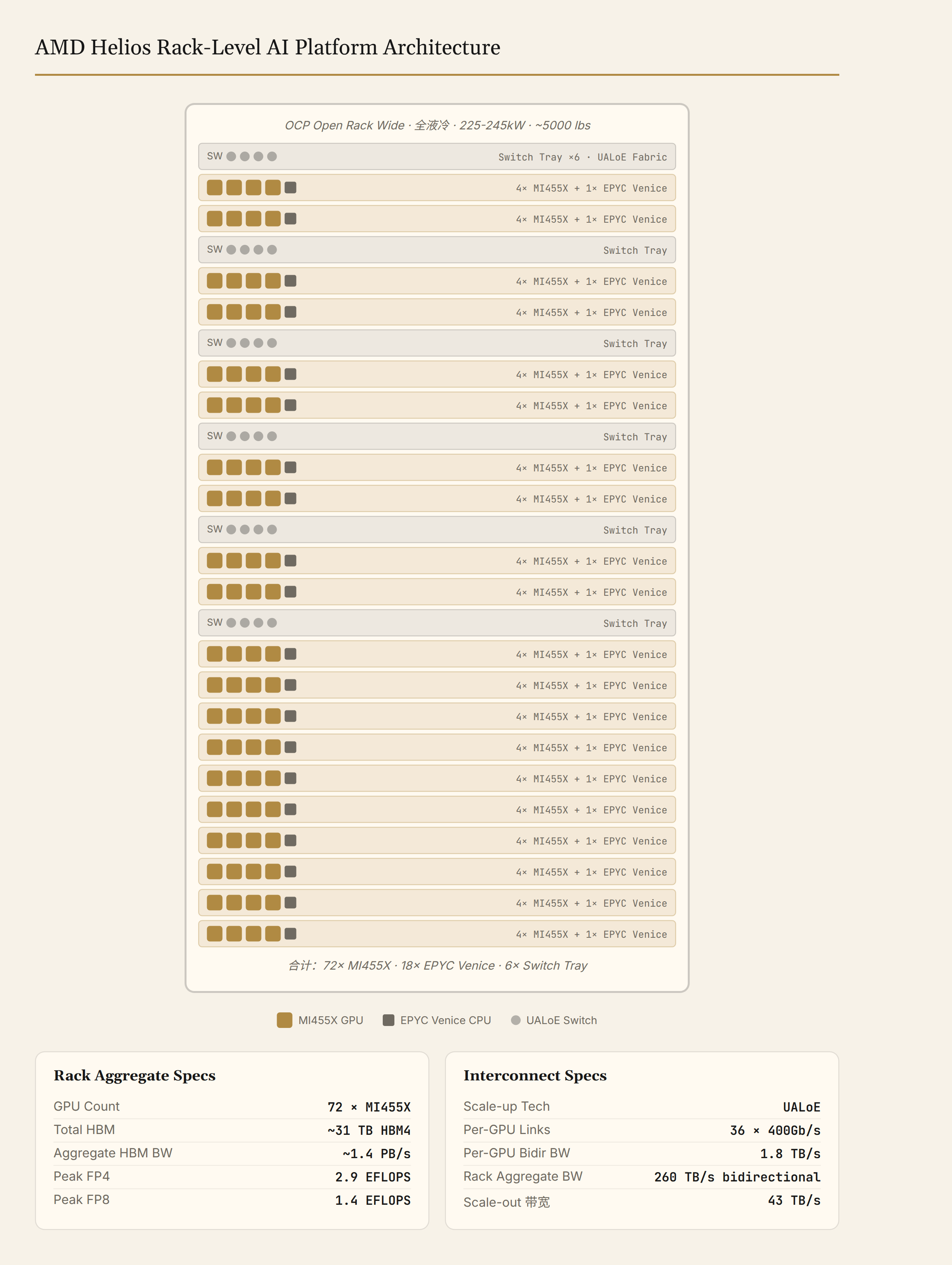
- 18 compute trays, each with 4 MI455X GPUs + 1 EPYC Venice CPU
- 6 switch trays running the UALoE scale-up fabric
- Full liquid cooling, with copper cold plates covering every GPU
- Entire rack weighs approximately 5,000 lbs (2,268 kg), power consumption 225–245 kW
- OCP Open Rack Wide dual-wide rack form factor
Rack-level aggregate specifications:
| Dimension | Value |
|---|---|
| GPU count | 72 MI455X |
| Total rack memory | ~31TB HBM4 |
| Aggregate memory bandwidth | ~1.4 PB/s |
| Peak compute | 2.9 EFLOPS FP4 / 1.4 EFLOPS FP8 |
| Scale-up bandwidth | 260 TB/s (bidirectional aggregate, 72 × 1.8 TB/s bidirectional) |
| Scale-out bandwidth | 43 TB/s (aggregate) |
| Host CPU | 18 EPYC Venice (Zen 6, up to 256 cores) |
| AI NIC | AMD Pensando Vulcano 800 Gbps |
1.3 Three-Generation Roadmap
AMD also disclosed a three-generation supernode roadmap:
- Helios (2026): MI455X + Venice + Vulcano + Salina
- Helios 500 (2027): MI500 series + Verano + Como + Monza
- Helios 600 (2028): MI600 series + Ferrara + Palma + Levanzo
A cadence of one generation per year directly mirrors NVIDIA's annual release strategy.
2. MI455X: A Spec-by-Spec Comparison with Rubin
2.1 Core Specifications
MI455X is built on CDNA 5 architecture, with 320 billion transistors, using a chiplet design:
- 8 XCDs (Accelerator Complex Dies), TSMC 2nm (N2 GAA) process
- 2 FCDs (Fabric and Cache Dies) + 2 IODs (I/O Dies), TSMC 3nm (N3P) process
- CoWoS-L advanced packaging, 12 HBM4 stacks
Spec-by-spec comparison with NVIDIA Vera Rubin GPU:
| Dimension | AMD MI455X | NVIDIA Vera Rubin | Leader |
|---|---|---|---|
| HBM capacity | 432GB HBM4 | 288GB HBM4 | AMD +50% |
| HBM bandwidth | 23.3 TB/s | 22 TB/s | AMD +6% |
| FP4 peak compute | 40 PFLOPS | 50 PFLOPS | NVIDIA +25% |
| FP8 peak compute | 20 PFLOPS | 17.5 PFLOPS | AMD +14% |
| Process node | XCD 2nm + IOD 3nm | TSMC (specific node undisclosed) | AMD claims first 2nm GPU |
| Transistor count | 320B | Not disclosed | — |
| Interconnect | UALoE 36 links × 400 Gb/s, 1.8 TB/s bidirectional per GPU | NVLink 5, 1.8 TB/s bidirectional per GPU (NVIDIA published data) | Tied |
2.2 Architectural Changes
CDNA 5 introduces several key departures from CDNA 4:
Compute unit rename: CU (Compute Unit) is now WGP (Work Group Processor), with 256 WGPs total. Wave64 is replaced by Wave32, reducing instruction latency and register pressure—better suited for latency-sensitive inference workloads.
Cache restructure: The large-capacity Infinity Cache from the previous generation is gone, replaced by 96 MB per FCD for a total of 192 MB shared L2 cache (a 6× increase). Per-WGP Local Data Store (LDS) is doubled to 384 KB.
Multicast reads: New multicast memory operations enable a single memory read to broadcast to multiple WGPs simultaneously, reducing redundant memory traffic. The Tensor Data Mover gains direct transfer capability between LDS and DRAM, bypassing intermediate registers.
These improvements point in one direction: data movement efficiency for inference. AMD is not competing with NVIDIA on raw transistor count for peak FLOPS. Instead, it is optimizing the data movement paths.
2.3 Strategic Significance of the Memory Advantage
The 432GB vs. 288GB memory gap is more than a spec number. In large-model inference, memory capacity determines the size of model shards that can be loaded at once. More memory means:
- Less cross-GPU communication overhead (fewer model shards)
- Larger KV Cache space (supporting longer contexts and more concurrent requests)
- More MoE expert weights resident in memory
72 MI455X GPUs aggregate to 31 TB of memory—50% more than 72 Rubin GPUs at 20.7 TB. At large-scale inference deployments, this gap is material.
3. UALoE: The Engineering Bet on Ethernet for Scale-Up
3.1 What Is UALoE
UALoE (Ultra Accelerator Link over Ethernet) is Helios's most critical technology bet.
The core idea of UALoE: use standard Ethernet physical layer and switch silicon to carry the UALink protocol (the open accelerator interconnect standard defined by the UALink Consortium). Each MI455X has 36 UALoE links at 400 Gb/s each, delivering 1.8 TB/s bidirectional scale-up bandwidth per GPU—matching NVIDIA's published NVLink 5 figure of 1.8 TB/s bidirectional per GPU. All 72 GPUs form a unified address space via 6 switch trays.
3.2 Three Scale-Up Engineering Approaches Compared
There are currently three mainstream scale-up engineering approaches in the industry:
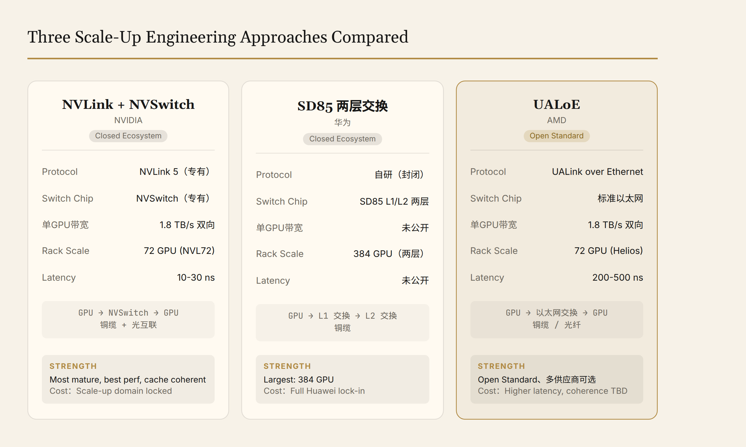
| Dimension | NVIDIA NVLink | Huawei SD85 Switch | AMD UALoE |
|---|---|---|---|
| Protocol | NVLink (proprietary) | In-house protocol | UALink over Ethernet (open) |
| Switch silicon | NVSwitch (proprietary) | SD85 L1/L2 two-tier switching | Standard Ethernet switch chips |
| Physical layer | Copper + optical | Copper | Ethernet (copper/fiber) |
| Ecosystem | NVIDIA closed | Huawei closed | OCP / UALink open |
| Per-GPU scale-up bandwidth | 1.8 TB/s bidirectional | Not disclosed | 1.8 TB/s bidirectional |
| Rack scale | 72 GPUs (NVL72) | 384 GPUs (two-tier switch) | 72 GPUs |
NVIDIA's NVLink is the most mature solution. Proprietary protocol + proprietary switch silicon delivers the best performance, but the entire scale-up domain is fully locked into NVIDIA. Huawei's SD85 achieves 384-GPU interconnect with in-house switch chips, leading in scale-up domain size, but is equally closed.
AMD has chosen a different path. UALoE uses standard Ethernet switch silicon to carry the UALink protocol—in principle, any UALink-compliant switch chip can participate. The logic mirrors x86 replacing RISC servers and Linux replacing Unix.
3.3 The Engineering Cost of Ethernet for Scale-Up
Using Ethernet for scale-up is not a free lunch. Ethernet switch chips are designed for general-purpose networking, not for the high-frequency, low-latency, high-volume traffic patterns of GPU-to-GPU communication. Key challenges:
Latency: Commercial Ethernet switch chips typically have port-to-port latency of 200–500 ns. NVSwitch, based on public data, operates in the 10–30 ns range. For latency-sensitive operations like AllReduce in large models, this gap compounds.
Traffic management: GPU scale-up traffic is dominated by elephant flows (large bulk data transfers), requiring lossless Ethernet support (PFC, Priority-based Flow Control; ETS, Enhanced Transmission Selection). Whether Ethernet switch chips' buffer management and traffic engineering capabilities can match the bursty patterns of GPU communication requires empirical validation.
Coherence model: NVSwitch + NVLink implements hardware-level cache coherence between GPUs—the CUDA programming model can directly perform cross-GPU memory access. Whether UALoE achieves hardware-level coherence or relies on software-layer coordination has a direct impact on programming complexity.
AMD has introduced a disaggregated DMA architecture to mitigate these issues: front-end units automatically split transfer requests and distribute them to back-end units at the UALoE interface, without communication libraries needing to be aware of the underlying topology. This reduces software-layer intrusion, but the physical constraints of latency and coherence at the lower level remain.
3.4 UALoE Protocol Stack: FLIT Switching over Ethernet
To understand UALoE's engineering choices, we need to unpack its protocol stack structure.
The UALink protocol uses FLIT (Flow Control Unit) switching, not the variable-length packet switching of traditional Ethernet. The core differences:
| Dimension | Traditional Ethernet Packet | FLIT Switching |
|---|---|---|
| Data unit | Variable-length frames 64B–16KB | Fixed-length FLITs (UALink 1.0 spec defines FLIT size as 256 bytes) |
| Buffering | Large packets require large buffers | Small-capacity slice buffers, low latency |
| Pipeline | Parse header → route → forward | Slice parallel processing, single-cycle forwarding |
| Header handling | Header and data travel together | Header FLITs separated from Data FLITs |
UALink's FLIT switching belongs to the same technology category as NVLink and PCIe. All are designed for GPU/xPU interconnects, distinct from general-purpose Ethernet packet switching. FLIT switching's advantages are low latency and high throughput; the trade-off is less flexibility compared to variable-length packets.
UALoE's core innovation is running UALink's FLIT switching over Ethernet's physical layer (PHY). This means:
- The physical layer reuses Ethernet's mature SerDes, electro-optical conversion, and cable ecosystem (mature, low-cost, multi-vendor)
- The link layer and above use UALink's FLIT protocol (low latency, GPU-optimized)
- Switch chips must support FLIT forwarding, not standard Ethernet L2/L3 forwarding
UALink's design goal is to concentrate processing at the switch side, reducing protocol overhead (area and power) at the xPU end. This benefits GPU vendors—they don't need to stuff a large network controller into the GPU package.
UALink roadmap (source: UALink Consortium public information and AMD's Advancing AI 2026 technical presentation):
| Version | Spec status | Expected hardware |
|---|---|---|
| UALink 1.0 | Released | Switches/accelerators late 2026 – early 2027 |
| UALink 2.0 | Released (includes 4 specification documents) | Hardware late 2027 – early 2028 |
| UALink 3.0 | Expected 2027 announcement | Hardware an additional year later |
Helios's UALoE is based on UALink 1.0. This means Helios's scale-up fabric is a first-generation product in terms of protocol maturity—fundamentally different from NVLink 5, which is a mature product refined over five generations.
3.5 ByteDance EthLink: An Alternative Ethernet Scale-Up Approach
ByteDance published its GPU Scale-Up Interconnect Technology White Paper in 2025, proposing the self-developed EthLink protocol. Like AMD's UALoE, EthLink is built on Ethernet, but the protocol stack design differs significantly.
The EthLink protocol stack has two layers:
- Scale-Up Semantic Layer: Includes upper-layer GPU operations and a scale-up transaction layer. GPU operations support a dual-semantic model: Load/Store (synchronous, small data transfers, latency-sensitive) and RDMA (asynchronous, large data transfers, bandwidth-prioritized). The transaction layer defines Memory Read, Memory Write, and similar operations, analogous to PCIe's transaction model.
- Scale-Up Network Layer: Handles Ethernet physical transport, with several key optimizations:
- LLR (Link Layer Retry) for reliable transport
- CBFC (Credit-Based Flow Control) for lossless networking
- Optimized packet header OEFH (Optimized Ethernet Frame Header) to improve payload efficiency
- RS-272 FEC (Forward Error Correction) with a low-latency coding scheme
Key EthLink design decisions:
Cache Coherency is guaranteed by system software, not by network hardware. Here, coherence refers to consistency of cache copies across multiple GPUs: NVLink maintains coherence through hardware protocols (extensions similar to MESI), while EthLink delegates this responsibility to system software, which ensures coherence through cache flush/invalidate or memory barrier operations. The cost is increased software overhead and latency; the benefit is simplified network hardware.
Dual-semantic model: The Load/Store path is for synchronous accesses initiated directly by GPU compute engines, with latency in the hundreds of nanoseconds and small data volumes (32/64-bit address width). The RDMA path is for asynchronous transfers initiated by an RDMA Engine, prioritizing bandwidth for larger data volumes (cache-line-level 64–256 bytes up to bulk transfers). The two paths operate in parallel, forming a pipeline.
Maximum support for 1,024 GPU nodes—far exceeding Helios's 72 and NVL72's 72.
3.6 Four Scale-Up Protocol Approaches Compared
Putting NVLink, UALoE, EthLink, and Huawei's in-house protocol side by side for a protocol-level comparison:
| Dimension | NVLink 5 | UALoE (AMD) | EthLink (ByteDance) | Huawei SD85 |
|---|---|---|---|---|
| Switch type | FLIT | FLIT over Ethernet PHY | Variable-length packet + optimized header | In-house protocol |
| Semantic model | Load/Store + Cache Coherent | Load/Store (inferred) | Load/Store + RDMA | Not disclosed |
| Coherence | Hardware-level | Not fully specified¹ | Software-guaranteed | Not disclosed |
| Reliability | Link-layer retransmission | Link-layer (FLIT) | LLR + CBFC | Not disclosed |
| Maximum domain | 72 GPUs | 72 GPUs (Helios) | 1,024 GPUs | 384 GPUs |
| FEC | Lightweight | Follows Ethernet | RS-272 low-latency | Not disclosed |
| Ecosystem | NVIDIA closed | UALink Consortium open | ByteDance-led, intended industry collaboration | Huawei closed |
| Maturity | 5th-gen in production | 1st-gen (delivery late 2026) | Whitepaper stage | Deployed |
¹ The coherence definition in the UALink 1.0 specification has not been fully disclosed; this assessment is based on currently available information.
Several specifications for Huawei SD85 cannot be obtained due to information restrictions; only publicly available data is listed.
Key judgments:
Coherence is the biggest divergence point. NVLink's hardware-level Cache Coherence lets the CUDA programming model directly perform cross-GPU memory access without upper-layer software concerns. EthLink has explicitly chosen software-guaranteed coherence, reducing network hardware complexity but increasing software overhead. AMD has not fully specified UALoE's coherence strategy—this is a critical point pending validation.
Switch type determines the latency ceiling. FLIT switching (NVLink, UALoE) inherently achieves lower latency than variable-length packet switching (EthLink, standard Ethernet) in typical designs. EthLink narrows the gap through optimized packet headers and RS-272 FEC selection, but the single-cycle forwarding advantage of FLITs remains physical. This is why UALoE chose FLIT over Ethernet PHY rather than using native Ethernet packets directly.
Maximum domain scale. EthLink's 1,024 GPUs and Huawei's 384 GPUs far exceed Helios/NVL72's 72 in scale-up domain size. For ultra-large model training (which requires more GPUs participating in the same AllReduce), a larger scale-up domain reduces cross-domain communication. However, there is a physical constraint between domain size and per-GPU bandwidth: the number of ports and aggregate bandwidth of switch chips are finite.
The maturity gap is pronounced. NVLink is in its fifth generation, UALink 1.0 is first-generation, and EthLink remains at the whitepaper stage. From initial delivery to forming a convincing large-scale deployment track record typically takes a 12–18 month validation cycle. This means that even if UALoE and EthLink have superior design philosophies, they are unlikely to pose a substantive challenge to NVLink in production deployments before the second half of 2027.
3.7 Open vs. Closed: The Ecosystem Bet
AMD's UALoE wager rests on one premise: enough players do not want to be locked into NVIDIA's scale-up ecosystem.
The UALink Consortium's members include Google, Meta, Microsoft, and Intel, with AMD as a core driver. These companies share two characteristics: they operate hyperscale AI infrastructure, and they do not want to cede the scale-up domain entirely to NVIDIA.
If UALoE succeeds, the scale-up layer shifts from "NVIDIA monopoly" to "open standard + multi-vendor." This benefits AMD, benefits Ethernet switch chip vendors (Broadcom, Marvell), and benefits cloud providers' in-house silicon programs.
If UALoE fails, NVIDIA's NVLink moat deepens further. Once the scale-up domain is locked into NVLink, GPU selection, network architecture, and software stack are all bundled—migration costs become prohibitively high.
4. Competitive Landscape: Can MI450 Actually Take Market Share?
4.1 The Signal from the Anthropic Deal
The AMD-Anthropic partnership is the most important customer validation MI450 has received:
- Up to 2 GW of MI450-series compute capacity, with deliveries starting in H1 2027
- AMD strategic investment of up to $5 billion in Anthropic
- Anthropic's current primary compute comes from Google TPU and NVIDIA GPU
The signaling value of this deal exceeds the numbers. Anthropic is one of the most advanced AI model companies today (the Claude series), and its compute sourcing decisions set industry direction. Choosing AMD signals:
First, AI companies are taking compute supply chain diversification seriously. A three-source supply chain of Google TPU + NVIDIA GPU + AMD MI450 offers better negotiating leverage and supply security than any single vendor.
Second, MI450's inference capabilities have earned top-tier customer endorsement. Training validation will take more time, but inference (high memory capacity, high bandwidth, low-cost token output) is a battlefield where AMD can already compete.
Third, the $5 billion investment anchors a long-term partnership. AMD is not just selling cards—it is betting on a reshaping of the AI compute infrastructure landscape.
4.2 Training: The Biggest Open Question
AMD's official positioning is that MI455X targets both training and inference. But the industry knows that MI-series validation in training scenarios is far less mature than in inference.
Training demands more from GPUs than peak compute:
- Reliability under sustained operation (training runs routinely last weeks)
- Communication library maturity (NCCL's overwhelming advantage over ROCm communication libraries)
- Framework support depth (PyTorch / JAX deep optimizations for CUDA)
- Debugging and profiling toolchains
CUDA's ecosystem, built over more than a decade, still leads ROCm significantly in training-scenario toolchain maturity. Signal65's independent testing shows MI355X approaching or exceeding B200 in inference throughput, but public benchmark data for training scenarios is virtually nonexistent.
The critical test of the Anthropic deal lies here: if MI450 can prove itself in Claude training, AMD transcends being merely an "inference substitute" and becomes a true dual-workload platform. That validation will not appear until after H1 2027 deliveries.
4.3 Cost Economics
AMD used the Kimi K2 Thinking model for a TCO modeling demonstration at the launch. Under AMD's claimed best-case scenario, Helios delivers 30% higher tokens-per-dollar than NVIDIA Vera Rubin NVL72, with 10–15% higher single-GPU token throughput.
These figures come from AMD's own modeling, based on pre-production systems and pricing assumptions. Actual production performance remains to be validated. But the direction is reasonable: larger memory capacity + higher FP8 compute + OEM competition enabled by the open reference design all favor AMD on cost structure.
NVIDIA's premium stems from ecosystem lock-in and brand. If AMD can demonstrate a 30% inference TCO (Total Cost of Ownership) advantage, it will have material appeal for cost-sensitive deployments (sovereign AI, enterprise inference, edge training).
4.4 NVIDIA's Response
NVIDIA will not sit idle. Rubin is already accelerating, and Vera Rubin NVL72 is the direct Helios competitor. NVIDIA's advantages:
- CUDA ecosystem irreplaceability (training scenarios)
- NVLink + NVSwitch maturity and performance
- Full-stack integration from silicon to rack to software
- Customer relationships and developer community
NVIDIA's risk: the UALink Consortium already counts Google, Meta, Microsoft, and Intel among its members. If the open standard gains enough adopters, proprietary interconnects face long-term erosion pressure from open standards.
5. Connection to the WAIC Supernode Series
In our WAIC 2026 analysis series, we established an L1–L4 maturity grading framework for supernodes (see our previously published WAIC supernode enterprise decision analysis). Placing Helios in this framework alongside Huawei SD85 supernodes and the Lingqu full-stack:
| Dimension | Helios | Huawei SD85 | Lingqu (Huawei full-stack software) |
|---|---|---|---|
| Scale-up protocol | UALoE (open standard) | In-house (closed) | Kernel重构 (closed) |
| Switch topology | 6 switch trays, 72 GPUs | L1/L2 two-tier, 384 GPUs | MoE dataflow optimization |
| Ecosystem openness | OCP reference design, OEM/ODM participation | Full-stack in-house | Full-stack in-house |
| Validation status | Delivery begins late Q3 2026 | Deployed | Deployed |
| Programming model | ROCm (open) | CANN (opening up) | openFuyao (under development) |
Helios scores highest on the openness dimension: open reference design, open interconnect standard, open software stack. But openness does not equal maturity. The gap between ROCm and CUDA is real, and the gap between UALoE and NVLink performance is real.
From an enterprise decision-making perspective, Helios's value is this: it gives customers a viable path to supernode scale-up without choosing NVIDIA. The mere existence of this option changes NVIDIA's pricing power and customer negotiating leverage.
Conclusion
AMD has done the right thing with Helios: it has provided an open-standard alternative in the domain where NVIDIA is strongest—scale-up interconnect. UALoE is not the highest-performance scale-up solution, but it is the first NVLink alternative with top-tier customer endorsement (Anthropic 2 GW + Microsoft), a complete full-stack offering (GPU + CPU + NIC + DPU + software), and an open ecosystem (OCP + UALink).
MI455X's specs genuinely lead Rubin on the memory dimension (432GB vs. 288GB) and on FP8 compute (20 vs. 17.5 PFLOPS). But FP4 peak compute trails (40 vs. 50 PFLOPS), and the ecosystem gap in training is wider.
Core judgment: Helios will not displace NVLink's dominance in the short term. But it has opened a breach in inference scenarios and cost-effective deployments, and the Anthropic deal provides the first heavyweight validation of that breach. The real verdict lies in training: if MI450 proves itself in Claude training in 2027, AMD graduates from "inference substitute" to "dual-workload platform," and the AI silicon landscape changes materially.
UALoE's long-term significance may transcend the outcome of any single GPU generation. If Ethernet-based scale-up proves viable, NVLink's proprietary interconnect moat faces gradual erosion. This is not a one-product contest—it is a platform architecture contest.
Sources: AMD Advancing AI 2026 official announcements, AMD official product pages, technical teardown coverage from Expreview / ITHome / KuaiTech, on-site reporting from ZAKER / Zhidx, Signal65 independent test reports. MI455X specifications from AMD official materials; Rubin specifications from NVIDIA official disclosures. Performance comparisons based on publicly stated peak theoretical values from both parties. Data as of July 29, 2026.