
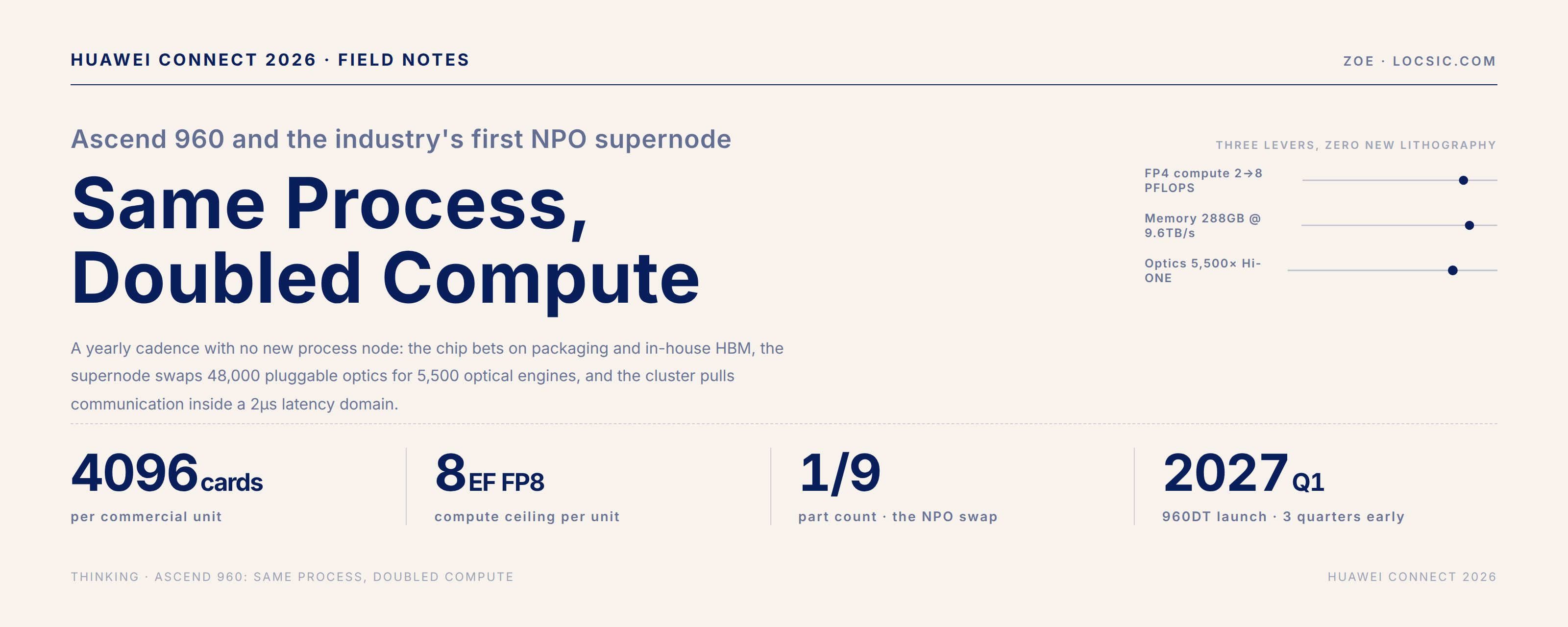
On the morning of September 17, the eleventh Huawei Connect opened in Shanghai. In his keynote, Rotating Chairman Wang Tao delivered numbers on three tiers. Ascend 960 chip development is running ahead of schedule, with the 960DT due in the first quarter of 2027, three quarters earlier than the roadmap announced a year ago. The Ascend 960 supernode runs 4,096 cards per system, the industry's first to bring near-package optics (NPO) into a supernode. Each system uses 5,500 in-house Hi-ONE optical engines in place of the 48,000 pluggable 800G optical modules it would otherwise need.
The process node did not change. Xu Zhijun stated the premise at the same event a year ago: build on the chip manufacturing processes China can actually obtain. Huawei has no new lithography windfall, and its promise of one generation a year with doubled compute in each does not rest on process advances. Folding and stacking inside the chip (the τ-law) and three tiers of leverage on the system side form two routes built on the same premise. This article takes apart where the doubling levers actually sit. The answer has three tiers: at the card level, packaging and memory move in-house; at the supernode level, the interconnect becomes optical engines; at the cluster level, communication overhead gets squeezed out of the training schedule.
The Single-Card 960: For the First Time, the Doubling Comes from Packaging, Not the Process Node
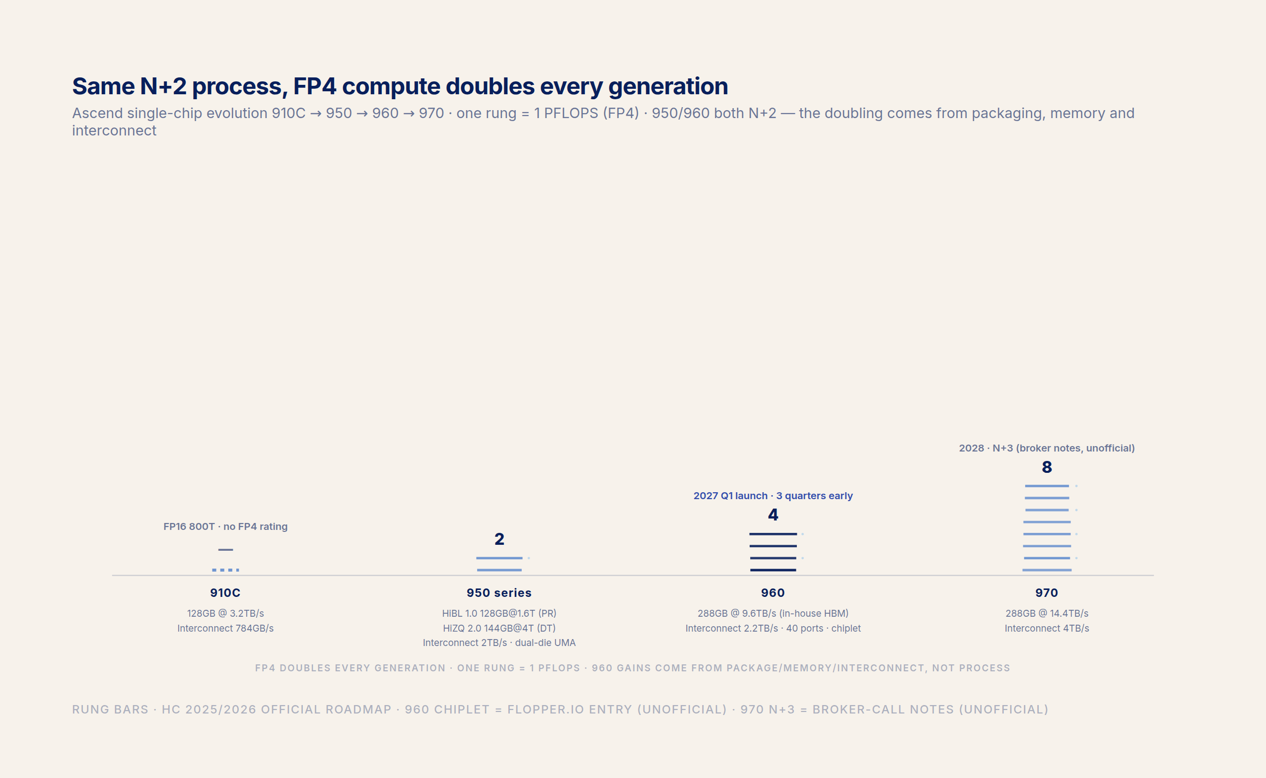
Start with the numbers on the official roadmap. Against the 950 series, the Ascend 960 doubles across the board on compute, memory capacity, memory access bandwidth, and interconnect port count: 2 PFLOPS of FP8 compute and 4 PFLOPS of FP4; 288 GB of memory at 9.6 TB/s of access bandwidth; 2.2 TB/s of interconnect bandwidth across 40 ports. The chip also introduces the in-house HiF4 four-bit precision format, which Huawei calls the industry's best 4-bit inference precision (no third-party replication yet).
The biggest change is in how the chip is built. The 950 series is a dual-die UMA design: two dies tied together by a high-bandwidth bus and presented to the operating system as a single device. The 960 moves to a chiplet-style multi-die package; the third-party spec database Flopper.io labels it the first chiplet design on Da Vinci v4, the fourth generation of Huawei's in-house NPU architecture, though that label is unofficial. Doubling chip-level compute no longer rides on transistor density; it rides on the number of dies inside the package. Structurally, this is the same move NVIDIA made going from Hopper's monolithic die to Blackwell's two reticle-size dies (chips close to the lithography mask limit), with Huawei one generation behind and bound to the process nodes obtainable in mainland China (supply-chain expert-call notes put the 950 and 960 at the N+2 node, with the migration to N+3 deferred to the 970 generation; unofficial information).
Memory is the bigger move at the card level. Starting from HiBL 1.0 on the 950PR (128 GB, 1.6 TB/s) and HiZQ 2.0 on the 950DT (144 GB, 4 TB/s), Huawei's in-house HBM has already completed two generational iterations. The 960's 288 GB and 9.6 TB/s double capacity and bandwidth at the same time, and the in-house memory stack absorbs the memory-side pressure of doubled compute. With Micron expecting the memory supply-demand imbalance to extend beyond 2028 and HBM supply tight, the in-house route answers the supply question and the cost question together.
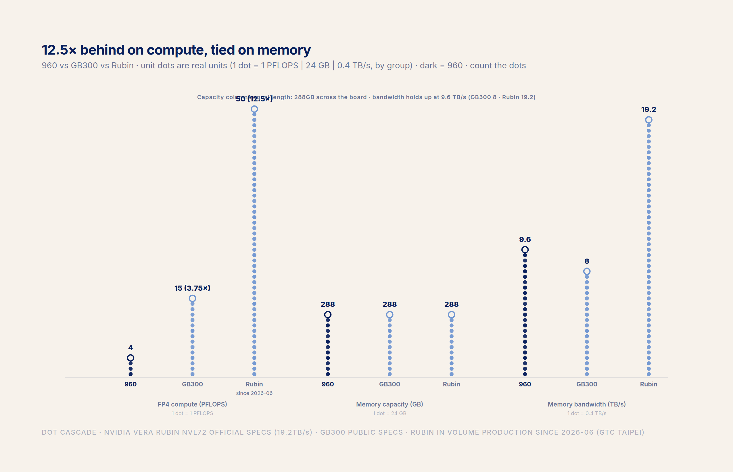
Set against contemporaneous NVIDIA products, the gap is still clear. GB300 delivers 15 PFLOPS of FP4 against the 960's 4, a 3.75× advantage; Rubin, in full production since June 2026 with 50 PFLOPS of FP4 per package, widens the gap to 12.5 times. Memory paints a different picture: the 960's 288 GB matches GB300 and Rubin, and its 9.6 TB/s of bandwidth beats GB300's 8 TB/s while trailing Rubin's 19.2 TB/s. Huawei does not chase compute parity at the card level. It uses capacity and bandwidth to hold the model and keep it fed, and leaves the compute gap for the system layer to close. This is the trade the 950 generation already proved out; the 960 carries it forward and doubles down on it.
4,096 Cards, One Computer: Three Ledgers for Moving Optical Interconnect into the Chassis
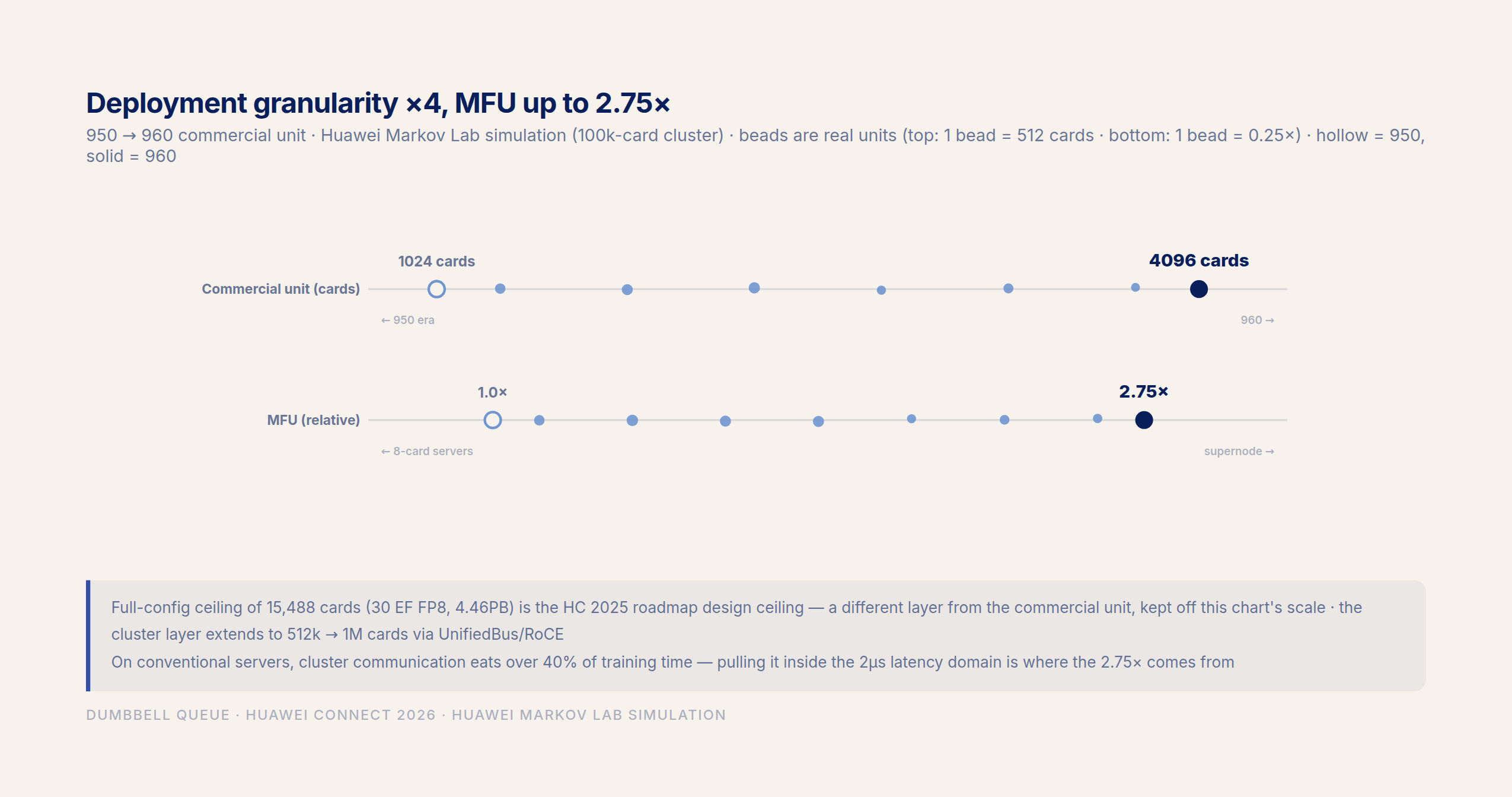
The commercial unit of the Ascend 960 supernode is 4,096 cards, delivering up to 8 EFLOPS of FP8 compute and 1 PB of HBM with round-trip latency as low as 2 microseconds; Huawei positions it for training and inference of 10-trillion-parameter models. For comparison, the 950 supernode's commercial unit is 1,024 cards. In the space of a year, commercial granularity grew fourfold. The 15,488-card full configuration on the Huawei Connect 2025 roadmap (30 EF FP8, 4.46 PB of memory) remains the design ceiling; the two figures coexist because they describe different levels.
The first constraint after a fourfold jump in granularity is interconnect. Copper was already near its engineering limit at the 950's 1,024-card scale: as SerDes (serializer/deserializer) rates climb further, electrical reach shortens and cable bulk swells, so 4,096 cards require pushing the optical engines right up against the package. Huawei compresses this generation's interconnect stance into one phrase: "near copper, far optics." That is where Hi-ONE sits. It is HiSilicon Optoelectronics' high-density optical engine platform, 200G per lane and 7.2 Tbps of transport capacity per engine; Huawei calls it the industry's first mass-produced NPO product and the only design with a built-in light source.
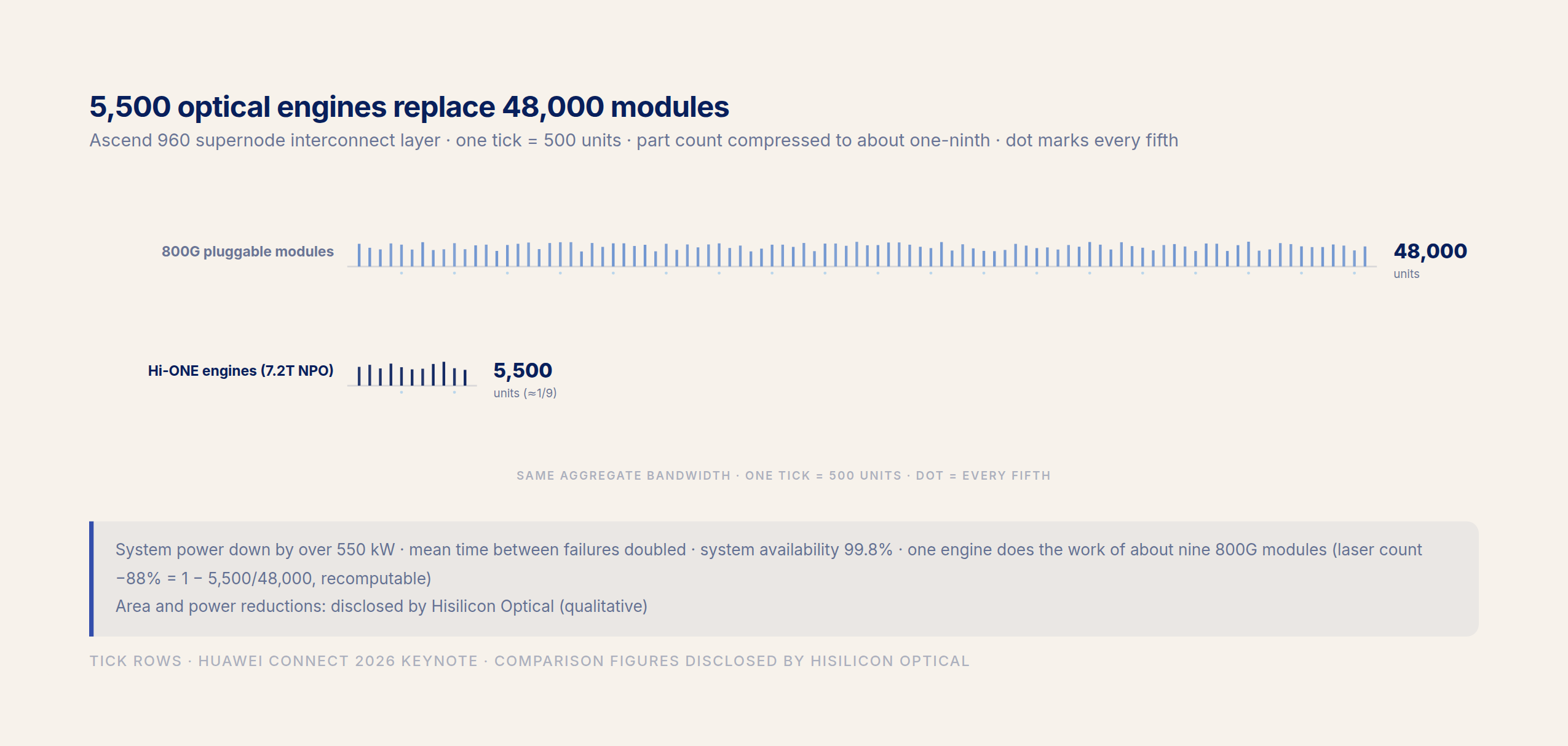
The first ledger is component count and power. The bandwidth carried by those 5,500 7.2 Tbps engines would otherwise require 48,000 pluggable 800G modules: component count compresses to roughly one-ninth, system power falls by more than 550 kW, mean time between failures doubles, and system availability reaches 99.8 percent. Per engine, one Hi-ONE stands in for about nine 800G modules, laser count drops by about 88 percent, and footprint and power fall sharply as well (per HiSilicon Optoelectronics' disclosure).
The second ledger is the technology-route tradeoff. Mainstream optical interconnects keep their high-power light sources external and couple light into the silicon photonics engine over polarization-maintaining fiber, on the grounds that sources degrade at high temperature and their reliability is hard to control. HiSilicon instead builds the InP (indium phosphide) high-power light source directly into the engine and uses aluminum quantum-well material to improve high-temperature carrier confinement; measured power drift over 10,000 hours stays within ±10 percent, better than the industry's customary ±20 percent. A WDM (wavelength-division multiplexing) architecture compresses 36 transmit and 36 receive lanes into 18 + 18 fibers. A DSP-free linear-drive design (no digital signal processor in the path) cuts transport latency from 110 nanoseconds to the 10-nanosecond class (per HiSilicon Optoelectronics). Integrated StarSensor fault diagnostics pin optical-link failures to minute-level detection and centimeter-level accuracy, aimed squarely at the transient service outages that optical-link failures cause in AI compute clusters.
The third ledger is the logic of NPO displacing CPO (co-packaged optics). The industry has mostly treated NPO as a transitional form on the way to CPO. CPO seals the optics and the switch chip on the same substrate, maximizing integration, but a failed optical engine cannot be replaced on its own. NPO packages the optical engine separately and deploys it next to the chip, preserving pluggability and serviceability. In choosing NPO, Huawei is balancing yield, power, and maintenance cost. For a 4,096-card system carrying 5,500 optical engines, serviceability decides outright whether the scale is viable.
Cluster Economics: Communication Eats Over 40 Percent of Training Time, and Topology Pens It into the Supernode
Above the card and the supernode, the 960 generation also settles the cluster-level ledger. Simulations by Huawei's Markov Lab show that a 100,000-card cluster built from 4K-card supernodes reaches 2.75 times the model FLOPs utilization (MFU) of a 100,000-card cluster built from eight-card servers. Under the conventional server architecture, intra-cluster communication consumes more than 40 percent of training time. That 2.75-times figure comes from topology: expert-parallelism traffic in MoE models is fenced entirely inside the supernode's 2-microsecond latency domain. Above that, multiple supernodes can network through UnifiedBus (Lingqu, Huawei's self-developed interconnect protocol) or RoCE. Huawei quotes a maximum cluster size of 512,000 cards, extendable to 1 million with multi-rail topology.
The supporting hardware for this economics arrived in the same launch. The Kunpeng supernode scales to a maximum of 4,096 nodes and a 256 TB unified memory pool, forming a peer interconnect with the AI supernode that requires no protocol conversion. The OceanStor M900 provides a PB-scale KV-cache tier direct-attached over UnifiedBus, using hybrid media and optimized Retention algorithms to lift SSD read/write endurance to 16 times, a multi-tier KV-cache architecture aimed at long-sequence agent inference. Weights sit in supernode memory, KV state sinks into the storage tier, and communication stays inside the optical domain: three media, each doing its own job.
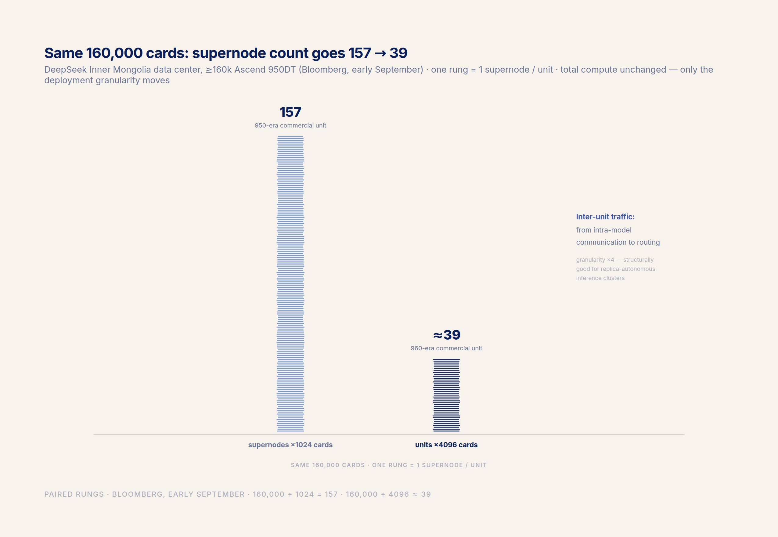
A concrete example. Bloomberg reported in early September that DeepSeek plans to deploy at least 160,000 Ascend 950DTs at a datacenter it is building in Inner Mongolia. At the 1,024-card commercial unit, that is 157 supernodes; at this generation's 4,096-card granularity, the same scale maps to about 39 units. With deployment granularity four times larger, inter-unit interaction degrades from intra-model communication to request routing, and each unit is a computer that carries an entire model. For inference clusters designed around replica autonomy, this is a structural tailwind.
The Software Stack Did Not Start with the 960: The 950's Report Card
To judge the 960's ecosystem starting point, look at what happened with the 950 this year.
DeepSeek V4 was the watershed. Exactly two software stacks delivered full Day 0 inference support on launch day: CUDA and Huawei CANN. A trace-level teardown of the 950DT running DeepSeek V4-Flash by SemiAnalysis (as relayed by media) shows CANN achieving three levels of execution overlap in a 16-way expert-parallel deployment: compute overlapping collective communication, shared-expert compute hidden underneath routed-expert compute, and indexing and compression operations overlapping each other. This is engineering capability at the instruction-scheduling level, beyond adaptation that merely gets the model running. V4 was coordinated with Ascend from the architecture-design stage: its attention mechanism, MoE quantization scheme, and expert-parallelism communication design all account for Ascend's execution paths. Joint definition of model and silicon has produced its first large-scale instance inside a domestic Chinese stack.
The market's signals are more direct. ByteDance has locked in about half of 950-series capacity, with Alibaba and Tencent following in the hundreds of thousands of chips. China Mobile has opened a supernode equipment procurement for 6,208 cards (776 compute nodes). On September 10, Bloomberg Businessweek, citing people with knowledge of the matter, reported that HBM costs had pushed the Ascend 950DT's price up about 60 percent over the past three months, to RMB 250,000. The price rise is evidence of a supply bottleneck, and equally of overheated demand. When DeepSeek cut V4-Pro pricing to a quarter, it also previewed that Pro prices would come down substantially again once Ascend 950 supernodes ship in volume in the second half of the year. The chain linking inference cost to domestic-chip supply can now be read directly off public pricing.
This is the starting point the 960 inherits: more than 5,200 monthly-active developers on CANN, more than 40 models natively trained on Ascend, and more than 20 million openEuler installations. Huawei officially calls it the only domestic technology route that supports pretraining.
The 2027 Matchup: A Competition Offset by Half a Generation
On the timeline, the 960DT's first quarter of 2027 does not line up against Rubin. That statement is about chip cadence; systems run on a separate clock, with the Atlas 860 air-cooled and Atlas 960 liquid-cooled supernodes planned for the second and third quarters of 2027 respectively. Rubin entered full production in June 2026 and starts going into racks at major cloud providers in the second half of the year. The 960's true head-to-head opponent is the Rubin Ultra NVL576 in the second half of 2027 (four dies per package, about 100 PFLOPS FP4, 1 TB of HBM4e, 600 kW Kyber racks).
The structure of the competition is offset. At the card level, the 960's 4 PFLOPS against Rubin Ultra's roughly 100 is a gap of about 25 times; at the system level, the 960 supernode's 4,096-card scale-up domain against the NVL576's 576 dies turns the ratio around at roughly seven to one. Huawei trades scale-up domain size for single-card density. Both numbers are real; which one dominates depends on which layer is taken as the baseline. At bottom this is a contest between two ways of organizing resources: one pushes compute density toward the packaging limit, the other pushes coordination scale toward the optical-interconnect limit.
Geopolitical boundaries carve out the markets for this offset competition. Because of export controls, the domestic market naturally sits within the Ascend ecosystem. Overseas, Huawei is exploring markets such as Malaysia and Egypt, and South Korean channels plan to bring in the 950DT, 950PR, and the Atlas 950 SuperPoD in the fourth quarter of 2026 (per ETNews). A Morgan Stanley research note (as relayed by media) projects China's AI chip market at RMB 646 billion by 2030. The 960's main battlefield is markets where inference demand is exploding while NVIDIA supply is constrained.
The Risk List: Capacity, Yield, and Unproven Training
First, in-house HBM capacity. The 950DT's roughly 60 percent price rise over three months says the bottleneck has already reached the supply side. How fast in-house HBM ramps decides whether the 960's doubling stays on paper or becomes a doubling in deliveries; this is the hardest constraint in the entire roadmap.
Second, NPO yield and engineering validation at scale. High-lane-count silicon photonics engines are sensitive to manufacturing tolerances. Hi-ONE today relies mainly on MZ (Mach-Zehnder) modulators, with denser schemes such as microring resonators sitting later on the roadmap. In a 5,500-engine system, any defect in yield, coupling, or maintenance gets multiplied by 5,500. The first mass-produced NPO label currently rests on the vendor's own account; large-scale field data has not been made public.
Third, training capability remains unproven. What the 950 generation validated was inference and decode. Training of domestic frontier models still leans heavily on high-end NVIDIA chips (per Bloomberg and other media). The T in 960DT stands for Training; whether it can carry the main training load of a frontier-scale cluster in 2027 is this generation's real exam.
Fourth, two mutually inconsistent number sets. For the 960 supernode's improvement over the 950, Huawei Connect 2026 published 2.3 times for training and 2.5 times for inference on a 10-trillion-parameter model. Huawei Connect 2025 published 3 times for training and more than 4 times for inference. The two sets use different reference frames, presumably reflecting the difference between commercial-unit and full-configuration baselines; this article retains both and awaits Huawei's clarification.
Summary and Judgment
This article has taken apart the Ascend 960's three-tier structure: the card doubles through chiplet packaging and in-house HBM, the supernode pushes commercial granularity to 4,096 cards on NPO optical engines, and the cluster squeezes communication overhead out of training time through topology. None of the three tiers depends on process advancement. Under a process ceiling, this amounts to a complete track change in how compute grows.
Three judgments:
First, the 960 is the first full delivery of the system-defined silicon route. System-defined silicon means chip specifications and tradeoffs are derived backward from what whole systems and clusters need: the system requirement comes first, the chip specification follows. The 950 validated joint definition across software stack and models; the 960 brings interconnect into the in-house product line as well (Hi-ONE, UnifiedBus, and M900). This generation co-developed 11 key chips around the supernode, covering compute, interconnect, and storage. Chip design is now reverse-derived from system topology, and the ceiling of this model sits on the in-house HBM capacity curve.
Second, NPO is shifting from transitional form to main path. With the first mass-produced NPO supernode, Huawei shows that optics inside the chassis can balance all three ledgers at once: power, density, and operations. NVIDIA is betting on the higher-integration CPO. Between 2027 and 2028, supernode interconnect will split into two routes, serviceable versus maximum density, and choosing between them is at heart a contest of operations economics. Operations is home turf for a company that has spent more than thirty years in the connectivity business.
Third, China's inference-compute cost curve has begun moving independently of NVIDIA's pricing system. The 950 already showed the shape: V4-Pro cut to a quarter of its price, and DeepSeek's token share in Vercel AI Gateway statistics rising from under 1 percent to 17 percent in May, past OpenAI. Once the 960 supernode design is locked, domestic inference costs will track in-house HBM, NPO optical interconnect, and electricity prices, decoupled from GPU market prices. The slope of that curve gets its first direct reading in 2027, from DeepSeek Pro pricing after the Ascend 950 supernode ships in volume.
What to watch next: first, whether the 960DT ships on schedule in the first quarter of 2027, given the execution risk inherent in a three-quarter pull-in. Second, the actual size of the DeepSeek Pro price cut once the 950 supernode ships in volume in the second half of 2026, already previewed officially. Third, Hi-ONE's generational evolution and the industry spread of NPO standardization (the OPEN NPO multi-source agreement, the OIF standards project). Fourth, how the first overseas supernode lands in South Korea in the fourth quarter of 2026. Fifth, when the 15,488-card full configuration makes its official debut.
Sources
- Huawei Connect 2025, full text of Xu Zhijun's keynote (Huawei official site, 2025-09); Huawei launches the Ascend 960 supernode (Huawei official site, 2026-09-17); on-site coverage of Wang Tao's keynote (STAR Market Daily, National Business Daily, Guancha, China Science and Technology Net, Eastmoney; 2026-09-17)
- Reuters: Huawei to launch two new AI chips in 2027 (2026-09-17); report on the Ascend 950DT price increase (2026-09-10)
- Bloomberg Businessweek: Huawei raises prices on its most advanced AI chips (950DT up about 60 percent in three months, to RMB 250,000) (2026-09-10, relayed via Sina Finance and Weibo)
- SCMP: Huawei unveils latest tech to boost AI power (2026-09-17)
- Bloomberg (relayed via Newtalk and Guancha): Ascend 960 preview, the Malaysia and Egypt markets, DeepSeek's 160,000-card Inner Mongolia deployment (2026-09)
- SemiAnalysis trace-level teardown of the Ascend 950DT inference architecture (relayed in full via InfoQ and NetEase Tech, 2026)
- HiSilicon Optoelectronics Hi-ONE: the IFOC 2025 launch (C114, ICC); CIOE 2026 chip-optics forum readouts (simpletechtrend); NPO industry deep dives (Hibor, 10jqka Finance)
- The τ-law V2 paper (He Tingbo, ChinaXiv:202605.00224v2) and this site's companion reads, Tau-Law V2: From Theoretical Framework to Production-Grade Evidence and After Folding, the Chip Runs Cooler
- NVIDIA: Vera Rubin in full production (GTC Taipei at COMPUTEX, 2026-06-01, announced by Jensen Huang; https://baijiahao.baidu.com/s?id=1866887647149058135); NVIDIA's site marks it as now in full production (https://www.nvidia.com/zh-tw/data-center/vera-rubin-nvl72/)
- NVIDIA Rubin specs: NVIDIA's official Vera Rubin NVL72 spec page; CES 2026 public information (36Kr, wccftech, vrlatech, and others); Rubin Ultra: Xueqiu, Baidu Baike (2026)
- Convequity, Flopper.io, ETNews, and the Morgan Stanley research note (as relayed by media)