
On September 4, He Tingbo posted the third paper in the τ-law series on ChinaXiv, with a title blunt enough to provoke: "Huawei's τ Chip Was Supposed to Melt?" The abstract states the stakes in its first sentence: "Heat is the sharpest concern on τ scaling law." The paper takes aim at the most concentrated objection after her May 25 keynote at ISCAS (the IEEE International Symposium on Circuits and Systems): logic folding lifts transistor density by 55 percent in a single generation, power per unit area should soar, and 3D stacking lengthens the heat-escape path for the lower silicon layer, so the chip ought to run hotter and burn more power. That is indeed the first reaction of anyone who knows the trade: folding means more power and harder cooling.
Three days later, the Mate XT2 carrying this chip was announced. Six days after that, Geekerwan published its full efficiency measurements. Once the two sides were set against each other, the result was inverted: the chip with 55 percent more transistor density draws substantially less power at equal performance, and on the Mate XT2 it held Genshin Impact at a full-frame 59.4 at high resolution on 5.4 watts for the whole device. Where the intuition went wrong is what the paper spends its entire length answering. Three questions follow: how the counterintuitive result holds up theoretically, what the measurements matched and what they proved right, and how much of the chip's headroom can still be read from the test data.
1. How the Counterintuitive Result Holds Up Theoretically
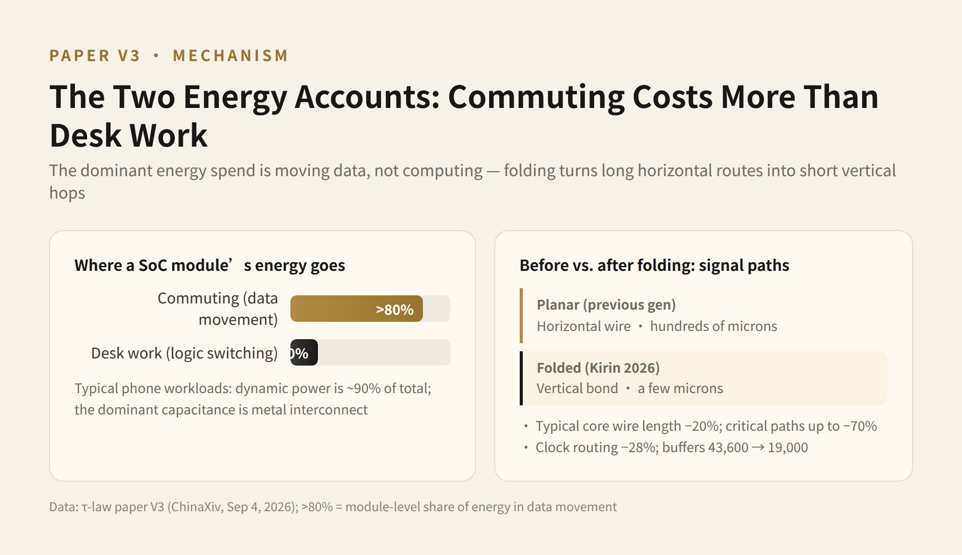
The argument begins with the composition of power. Most people picture chip power as transistor-switching power: a logic gate opens, closes, spends a little energy. The paper calls this "the work at the desk," the part that actually computes. What dominates is the other account: the energy spent moving data among memories, buffers, and compute units, which the paper frames as commuting. Its abstract compresses the point into one sentence every commuter already knows: "it is the travel that burns the majority of the energy, not the work at the desk." The quantified version: in large AI clusters, more than 80 percent of energy goes to data movement, and smartphone SoCs show the same imbalance to a milder degree. In typical phone workloads, dynamic power is about nine-tenths of total power, and the capacitance that dominates the dynamic-power equation comes mainly from metal interconnect, not from the transistors themselves.
Why interconnect is expensive deserves a full sentence. At advanced nodes the switching energy of a transistor is already low; the dominant term is the energy of charging and discharging wires. The longer the wire, the larger its accumulated parasitic capacitance, and every signal transition pays that capacitance once in each direction, with energy proportional to the capacitance itself. This relationship between wire length and energy was observed repeatedly as geometric scaling slowed, yet rarely treated as a central variable. The paper accordingly names shortening the signal travel distance as the first optimization target for power reduction.
Logic folding attacks exactly this account. The paper describes the technique as "taking a circuit that used to sprawl across a flat plane and folding it into vertically stacked tiers bridged by tiny vertical links so that signals travel shorter distances." The two silicon layers are joined by hybrid bonding, a process that fuses copper pads directly at the wafer level, with the bonding pitch setting the density of vertical connections. Kirin 2026 reaches a 1.5-micron pitch, so vertical connection points sit on average only microns apart. Signals that once traveled along horizontal wires hundreds of microns long now drop vertically through bonding pads. The paper gives three sets of engineering numbers: total wire length on a typical processor core shrinks about 20 percent, and critical paths by as much as 70 percent; on one processing module, clock routing shortens 28 percent and the clock-buffer count falls from 43,600 to 19,000. The clock network is among the busiest and most power-hungry networks on a chip; cutting its buffers by more than half saves precisely the energy of driving long wires.
After the wires shorten, the released margin passes through a square-law amplification. The area freed by folding holds more transistors, and for modules that scale directly, NPU (neural processing unit) and GPU (graphics processing unit) chief among them, double density means the same work can run at double the parallelism and half the frequency. Once frequency falls, each clock cycle allows more time for signals to propagate, and that timing slack lets supply voltage come down in step. Dynamic power is proportional to the square of voltage, so every fraction of voltage reduction is doubled in the power saving. The paper's flagship example: the previous NPU carried 1 large core plus 2 efficiency cores; the transistor margin released by folding let the new generation fit 4 large cores, and this wider array delivers 70 TOPS (trillion operations per second) at 0.7 volts. The previous generation topped out at 29 TOPS, under half that figure, and needed 0.85 volts to get there. The paper compresses the mechanism into one line: more hardware, running more gently, to do more work.
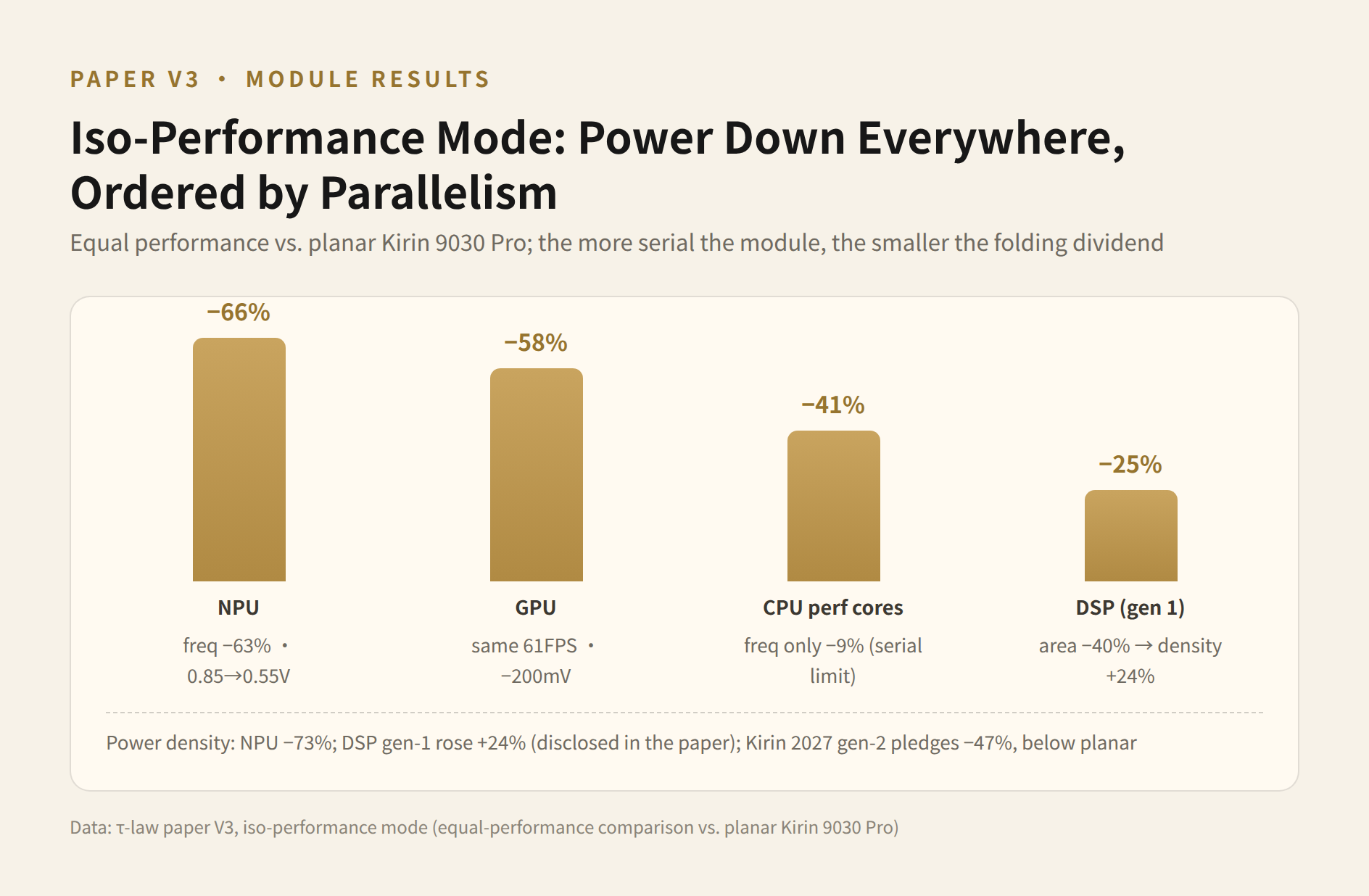
The boundary of the benefit is set by how serial the workload is. The paper invokes the hardware twin of Amdahl's law: the serial fraction of a program caps the gains from parallelism, and the serial critical paths on silicon likewise cap which regions can trade parallelism for voltage. NPU and GPU workloads are data-dense and highly parallel, so the folding dividend cashes in full. CPU (central processing unit) performance cores are serial-heavy, and the gains are structurally limited; the paper's own numbers put it at frequency down only 9 percent and power down 41 percent at equal performance. The DSP (digital signal processor) first-generation fold saved 25 percent of power. The gradient across four modules, NPU 66, GPU 58, CPU 41, DSP 25 percent, aligns with the parallelism of each workload. That alignment is itself evidence of internal consistency in the data.
The final link is a redirection of the thermal argument. The paper's own words: "We contend that critics are aiming at the wrong metric. What matters is not the heat, but the heat density — and, one level deeper, the junction temperature of transistors, which is the metric that actually governs speed, leakage, and reliability." Heat flows from the transistor junction through the chip's layers toward the heat sink, every segment of that path carries thermal resistance, and junction temperature is approximately power multiplied by thermal resistance plus ambient temperature; a chip does not fail from dissipating some number of watts, but when a junction climbs past its operating-temperature limit. Folding acts on this physical chain three ways: total power at equal performance falls first, cutting heat at the source; power spreads across two active silicon layers, lowering heat flux per unit volume; and thermal-aware placement interleaves hot and cold modules so hot spots do not stack vertically. Kirin 2026 only selectively folds the highest-payoff critical paths, and the paper explicitly labels the design conservative.
Two deliberately honest passages sit inside the argument. The DSP's first-generation fold cut power 25 percent but shrank area 40 percent, so power density rose 24 percent; the number is not hidden, and the repair pledge is written into the text: Kirin 2027's second generation redesigns the DSP for 47 percent power reduction and power density below the planar version. The other is the boundary statement, verbatim: "τ is a time scaling law, not an energy law. A folded system running faster but burning more power violates no time-scaling principle — yet it would drain your battery by lunchtime." The paper then closes the loop on why the real chip runs cool: "The cool-running Kirin happened because we deliberately spent the time headroom of folding on lower voltage and power. That trade is a companion discipline, not a free consequence of the law." And on the choice itself: "Physics permits both settings; discipline chooses the cool one."
The errors of intuition are now visible, three of them: counting logic gates while ignoring wire length; computing power per square millimeter while ignoring heat flux per cubic millimeter; watching total heat dissipation while ignoring junction temperature. The paper's closing image is Sisyphus, with one amendment: "this hill leads somewhere: every cycle leaves behind a chip that computes more and burns less."
2. Key Conclusions and Chip Metric Checkpoints
The paper's virtue is that most of its conclusions are checkable. Laid out as checkpoints, its claims give the audit an anchor:
- NPU: at the same 29 TOPS, frequency down 63 percent, voltage from 0.85 to 0.55 volts, power down 66 percent, power density down 73 percent. Full-speed mode delivers 70 TOPS at 0.7 volts
- GPU: at the same 61 frames per second, voltage down 200 millivolts and power down 58 percent. The full-speed figure is about a 42 percent gain
- CPU performance cores: at equal performance, frequency down only 9 percent and power down 41 percent. Peak frequency 3.1GHz, a derived gain of about 13 percent over the 9030 Pro's 2.75GHz, with the architecture unchanged
- DSP: first-generation fold cut power 25 percent and area 40 percent, raising power density 24 percent. The 2027 second generation pledges a 47 percent power cut and power density below the planar design
- Transistor density: from roughly 155 to 238 million transistors per square millimeter, a 55 percent increase
- Bonding: 1.5-micron hybrid-bonding pitch with 50 million vertical interconnects, roughly 10 to 15 percent of them carrying signals. Kirin 2027 silicon has reached a 1-micron pitch with more than 100 million interconnects
- Clock network: routing shortened 28 percent, buffers reduced from 43,600 to 19,000
- Roadmap: 720-nanometer pitch within three years with more than 200 million interconnects, pointing toward 480 nanometers thereafter; CPU peak frequency advancing from 3.1GHz toward and beyond 5GHz
The power and performance results of the first four can be approximated by device-level benchmarking, with silicon-level sub-items such as operating voltages and power density excepted. The last four depend on teardown analysis or internal data and cannot be verified by third parties for now.
3. The Audit: What Matched, and What It Proved Right
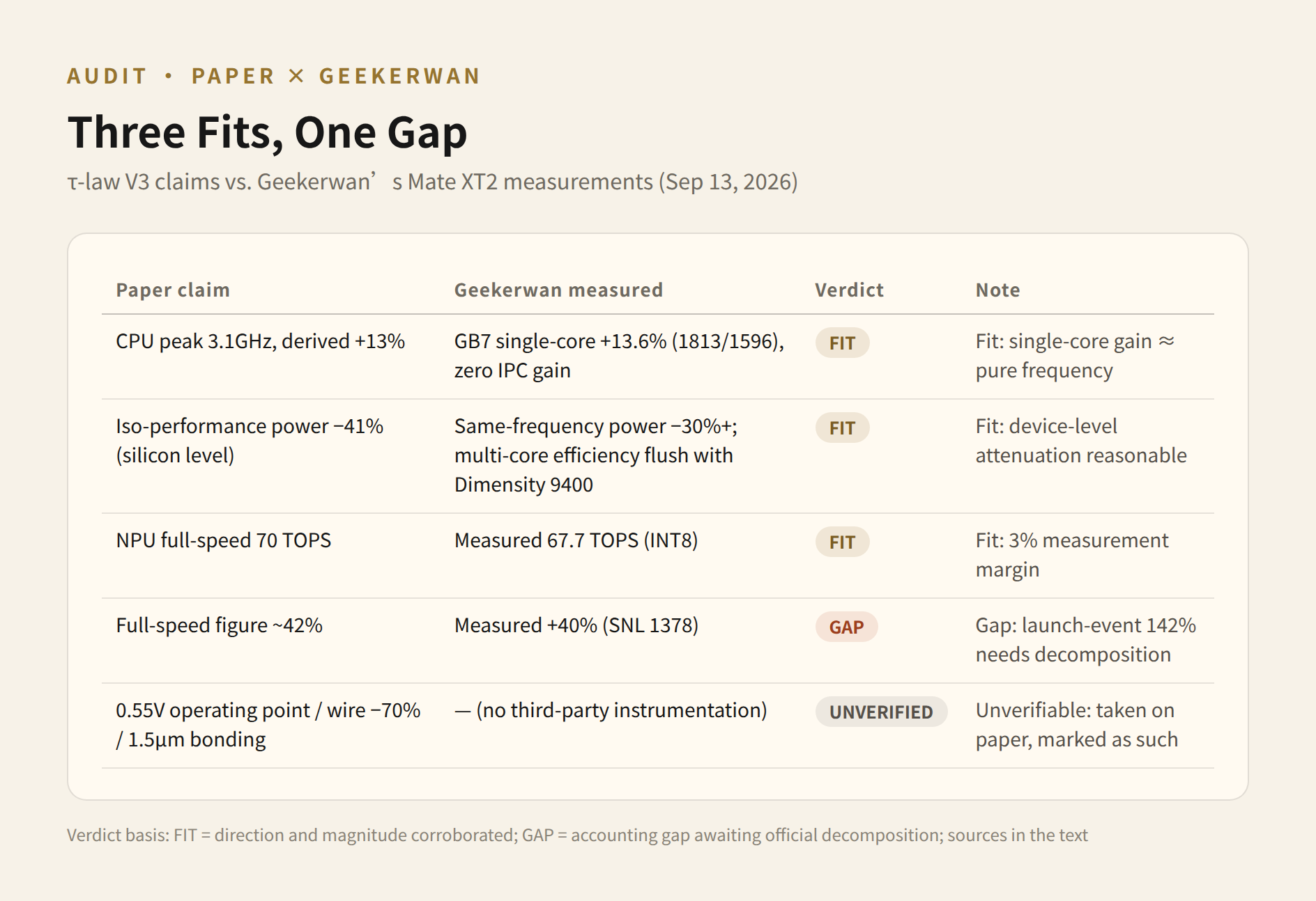
Geekerwan's full efficiency test of the Mate XT2, published September 13, went to real lengths methodologically: it ported native SPEC CPU 2026 and GeekBench 7 for HarmonyOS and swept the efficiency curves point by point across the frequency range. The paper's evidentiary protocol matters first, because it sets how the audit reads: each module reports two modes, one at equal performance with the previous generation and one at full speed, each carrying five data panels (performance, frequency, voltage, normalized power, normalized power density), with the planar Kirin 9030 Pro as baseline. Iso-performance mode answers what folding made cheaper; full-speed mode answers what the margin buys when spent on performance. The launch event's 142 percent and the paper's 42 percent differ by more than threefold, and the most natural explanation is that they belong to different modes and baselines. With that layer clear, the audit can proceed.
Single-core gain almost exactly equals frequency gain: architecture unchanged is directly proven, the serial limit corroborated. GeekBench 7 single-core 1813 against the 9030 Pro's 1596 is a 13.6 percent lift; the paper records the CPU peak frequency restored to 3.1GHz, which against the 9030 Pro's 2.75GHz is a derived gain of about 13 percent. Zero instructions-per-clock gain and a 13.6 percent single-core lift line up almost exactly. The pair of numbers matches two predictions at once: the paper's claim of an unchanged architecture is directly proven, with the zero IPC gain as its direct readout; and the predicted benefit gradient, in which the CPU is limited by serial workloads and collects no scale dividend, is corroborated on the device. Of all the audit points, this is the most persuasive.
Same-frequency power down more than 30 percent, efficiency up three tiers: the iso-performance power reduction is not just a number on paper. Geekerwan measured same-frequency power down more than 30 percent versus the 9030 Pro, with the multi-core efficiency curve sitting flush against the Dimensity 9400, the current first tier of smartphone efficiency. The paper's silicon-level figure is 41 percent for the CPU performance cores at equal performance. Thirty percent at the device level against 41 percent at the silicon level, with power delivery, peripherals, and the whole device in between, is a reasonable attenuation. Two generations took the chip from three tiers behind into the first tier, which matches the order of magnitude of the paper's self-calibration: density gains equivalent to three years of geometric scaling.
NPU measured at 67.7 TOPS against the paper's 70: the full-speed specification is real. The 3 percent gap is normal measurement margin against theory on the INT8 (8-bit integer) basis; running a 30-billion-parameter mixture-of-experts multimodal model on-device is the application-side corroboration of the same capability. The GPU scale route checks out as well: FP32 (32-bit floating point) throughput rose from 1.4 to 2.2 TFLOPS (trillion floating-point operations per second), and 3DMark Steel Nomad Light scored 1378, roughly 40 percent over the previous generation.
One gap: the launch-event-versus-paper accounting difference. The launch claimed a 142 percent gain in GPU rendering performance; the paper's full-speed figure is about 42 percent; Geekerwan measured +40 percent, matching the paper and sitting more than threefold below the launch claim. The 142 percent baseline most likely stacks a GPU architecture upgrade on top of logic folding itself, with folding accounting for only part of it; only Huawei can decompose that accounting. It is the one number left hanging in this audit.
A further batch of data cannot be verified by third parties: the NPU's 0.55-volt operating point, the 70 percent critical-path wire reduction, the 1.5-micron bonding with its 50 million vertical interconnects. The density accounting also needs its own label: 238 MTr/mm² (million transistors per square millimeter) is Huawei's own metric; a third-party conversion to the industry-standard Bohr basis gives roughly 175, against 313 for TSMC's N2, so calibrate the accounting before comparing across fabs. These are internal silicon figures, taken from the paper and marked unverifiable. The measurements deserve a discount of their own: GeekBench 7, though ported by Geekerwan, still had the prime and mid cores frequency-limited by system scheduling policy during the run, and the tri-fold's thermal structure constrains performance release, so the measured curves are likely a conservative floor, with third-party background data putting real performance 10 to 15 percent above the measured values.
4. Reading the Chip's Headroom from the Test Data
With the audit complete, the test data still holds five measures of headroom.
Frequency headroom. Geekerwan observed that the 3.1GHz step brought no significant power increase and still sits on the efficient segment of the curve, where higher frequency still buys real performance. The processor's frequency ceiling has not been reached; the paper's roadmap points CPU peak frequency toward and beyond 5GHz, and the current 3.1GHz leaves physical room on that path.
Efficiency headroom. One generation took the chip from three tiers behind into the first tier, and that is the conservative configuration's result: Kirin 2026 selectively folds only the highest-payoff critical paths, and the paper labels the design conservative. The full-speed 9050 Pro Max has not yet shipped; the bar-phone thermal envelope of the Mate 90 series is the precondition for its full release.
Measurement headroom. The frequency limits from GeekBench 7's lack of HarmonyOS adaptation, plus the tri-fold's form-factor thermal constraint, together depress measured values by 10 to 15 percent. The current readings are results compressed by the measurement environment, not the chip's actual ceiling.
Generational headroom. The 1-micron second-generation fold of 2027 has already taped out, with vertical interconnects crossing from 50 million past 100 million; the repair pledge on the DSP's 24 percent power-density increase rides on that generation. The bonding pitch roadmap runs toward 720 and then 480 nanometers, so the density path is long.
And one factor outside the chip. Geekerwan's conclusion emphasizes that with hardware and HarmonyOS 7 working together, the gaming experience has reached Snapdragon 8 Elite territory, with system scheduling contributing no less than the silicon itself. The chip's final potential is the product of what the chip can do and what the system can release.
Summary and Judgment
The chain of facts: the τ-law was proposed at ISCAS on May 25, grounded in six years and 381 shipped chip designs. The third paper took the thermal objection as its title on September 4 and answered it with Kirin 2026's module-by-module measurements. The chip shipped with the Mate XT2 on September 7, and Geekerwan completed the independent measurement on September 13. Three judgments:
1. The counterintuitive result has a real mechanism, and its name is trading density for voltage. What folding delivers is not an improvement at the level of the individual transistor — the fact that the entire 13.6 percent single-core gain came from frequency proves exactly that: what should not have changed (instructions per clock) truly did not, and what should have changed (efficiency) truly did. At equal performance the NPU drops 66 percent, the GPU 58, the CPU 41: voltage-squared arithmetic at work, and that arithmetic holds for any design that obtains double density. Folding also holds a second dividend that plain doubled density cannot claim: it cuts the commuting account itself, and the shortening of wires and clock networks comes directly from folding's vertical geometry. Stacked together, the two gains complete folding's value: this is the path Huawei holds in hand without next-generation lithography, delivering both doubled density and shorter wires.
2. The paper's writing is itself an industry signal. It discloses the DSP's 24 percent power-density increase, concedes the CPU's serial limitation, draws a boundary around the law (time scaling is not energy scaling), and writes the next generation's repair pledge into the body text. This is the writing of a route argument, not of a brochure. "Physics permits both settings; discipline chooses the cool one" is a sentence no marketing document would risk. The 142-versus-42 gap between the launch event and the paper makes the paper's numbers look more credible by contrast.
3. The final verdict belongs to the Mate 90, on two criteria. Every confirmation on the tri-fold comes from the conservative configuration plus a large heat-spreading surface; the full-speed 9050 Pro Max on a bar phone is the real stress test. And whether Kirin 2027's 1-micron second-generation folding delivers the promised DSP density repair is the most direct test of whether this route can compound generation after generation the way Moore's law did.
What to watch next, in order of verifiability: the full-speed efficiency curves of the 9050 Pro Max on the Mate 90 series. Measured data for Kirin 2027 (1-micron bonding, second-generation folding). Huawei's decomposition of the 142 percent claim. A re-test once GeekBench 7 is fully adapted for HarmonyOS.
(Facts and figures in this piece are current as of September 14, 2026, and are drawn from the paper and public reporting cited; the judgments are editorial opinion and do not constitute investment advice.)