
August 4–6, 2026. Santa Clara. The 20th edition of Flash Memory Summit.
The conference is now called Future of Memory & Storage. 3,500 attendees, 1,500 organizations, 350 speakers, 100 exhibitors. The rebrand isn't cosmetic — it's an industry admission that the old taxonomy no longer holds. When a single conference covers HBM vertical stacking, NAND doing TSV interconnect, SSDs accessed directly by GPUs, and CXL enabling memory to flow across servers, "Flash Memory Summit" is no longer an accurate name.
But the rename is surface. The real signal from FMS 2026 is a collective redefinition of storage architecture. Over the past year, multiple vendors independently began describing a storage architecture that departs from the traditional hierarchical model. SK Hynix and Sandisk's new HBF (High Bandwidth Flash) standard inserts a new media layer between HBM and SSD. Samsung describes its CXL memory modules with an "open PCIe/CXL fabric architecture." NVIDIA combines cuFile and SCADA into a GPU-to-SSD direct access channel. These signals converge on one trend: storage architecture is undergoing two simultaneous shifts — new media layers are being added (HBF/zHBM), but the hard boundaries between layers are dissolving (CXL lets memory flow across servers, ICMSP gives SSDs memory semantics, SCADA lets GPUs bypass the CPU to access storage directly).
Understanding this shift requires three dimensions: bus technology (what connects things), storage media (what nodes exist on the network), and protocol evolution (who controls scheduling).
I. Cracks in the Hierarchical Model
The old storage hierarchy is linear: GPU registers → L2 cache → HBM → DDR → SSD. Each layer has clear bandwidth and latency boundaries, and data moves between them. This model has held since the 1980s and fits a CPU-centric computing architecture.
AI inference broke it. Not by squeezing upward one layer at a time, but by tearing it apart from three directions simultaneously:
Direction one: Memory islands get bridged. Traditional server memory is bound to CPU memory channels and DIMM slots. In an 8-GPU server, the 2TB of DRAM is split across two CPU sockets, with NUMA cross-socket access latency doubling. When AI inference needs 500GB+ of KV Cache space, the problem isn't total capacity — it's that "the memory you need is on the wrong node." CXL (Compute Express Link, a cache-coherent interconnect built on the PCIe physical layer) liberates memory from the motherboard into a pooled resource. At FMS 2026, three CXL controllers were on display simultaneously — Samsung CMM-D, Marvell Structera, and Montage Technology MXC — the supply chain is approaching deployable status.
Direction two: SSDs are no longer "block devices." When NVIDIA's ICMSP (Inference Context Memory Storage Platform) defines SSDs as "first-class memory nodes for KV Cache," the SSD's role shifts from "file container" to "memory extension addressable by the GPU." Kioxia's GP1 delivers 10 million IOPS with 512-byte granularity access — these are not block-device performance characteristics. They are memory characteristics.
Direction three: New interconnects enter storage. The HBF standard adopted UCIe (Universal Chiplet Interconnect Express) as its interface to the processor — NAND storage stacks can now hang directly on the processor's in-package interface, just like HBM. UCIe isn't the only option; the HBF Alliance chose it for its industry consensus base. Samsung's zHBM takes its own wafer-bonding route, and NVIDIA's GPU-Direct SSD uses PCIe. The interfaces are diverging, but the direction is unanimous: storage media is moving closer to the compute unit.
Three directions combined: memory can be pooled (CXL), SSDs can be used as memory (ICMSP), and storage media can connect directly into the package (UCIe / zHBM). The hard boundaries of the hierarchical model are dissolving — data movement between media is no longer "overflow when the upper layer is full," but rather a scheduler selecting the optimal node based on latency budget and cost constraints. Meanwhile, new media layers (HBF, zHBM) are still being added, making the spectrum denser. The hierarchical model cannot describe this structure.
Micron provided an anchor data point during FMS: the share of memory (including HBM + DRAM + NAND) as a percentage of AI server system value has grown from roughly 10% three decades ago to nearly 50% today.[1] WSTS's spring 2026 forecast projected the global semiconductor market at $1.51 trillion, up 90% year-over-year, with memory chips growing 249.5%; the August Q2 update revised the full-year forecast upward to $1.655 trillion, up 108% year-over-year, with memory chip growth further revised to 302%.[2] The three major manufacturers have essentially locked in their 2027 DRAM and HBM capacity with strategic customers, with NAND allocations expected to be finalized by August.[3] The official FMS agenda featured a session titled "The Memory Supercycle 2026–2028."
When memory accounts for half of system cost, when storage chips grow 302% year-over-year, this industry is no longer a supporting actor to GPUs. It is redefining its own architecture.
II. Bus Technology: How Things Connect Is Being Rewritten
The physical foundation of networked storage is bus technology. At FMS 2026, interconnect technology across three layers underwent a generational leap simultaneously.
In-Package: Storage Media Connects Directly to the Processor
HBF connects to the processor via the UCIe interface. This is the first time storage has connected to a processor through a standardized in-package interface — previously, NAND always sat at the other end of the PCIe bus, behind a host controller.
UCIe's significance lies in standardizing physical connections between chiplets: die from different manufacturers can achieve plug-and-play through a unified interface, much like USB standardized device interfaces. HBF chose UCIe because it already has industry consensus; in principle, HBM, storage stacks, and accelerator die could all hang off the same interface ecosystem. But this isn't the only path — Samsung's zHBM uses wafer-bonding technology to vertically stack above the accelerator, taking the 3D integration route. Both paths shorten the distance from storage media to compute unit, but via different technologies.
In-Server: CXL 3.2 Moves from "Attached Memory" to "Multi-Host Sharing"
The first version of CXL solved memory expansion — giving servers more DRAM. By CXL 3.2, the core capability has become multi-host shared memory pools.
CXL supply chain status at FMS 2026:
| Vendor | Product | Key Specs |
|---|---|---|
| Samsung | CMM-D MD310 | CXL 3.2 / PCIe 6.0 / 256GB / 72 GB/s / EDSFF E3.S |
| Marvell | Structera series | Sub-microsecond access latency, multi-host dynamic memory pool sharing |
| Montage Technology | MXC CXL 3.2 Controller | Trial production stage, targeting CXL Type 3 memory expansion |
CXL's core value in AI scenarios is solving the "stranded memory" problem. Traditional server memory is bound to CPU channels and DIMM slots, provisioned for peak configuration. The result: some nodes are memory-starved while others sit idle. DDR5 16Gb DRAM contract prices rose from $4.80 in May 2025 to $37.50 in May 2026 — a 681% increase in one year. 256GB DDR5 server memory modules broke past ¥50,000. When memory is this expensive, leaving it idle is waste; pooling it is imperative.
CXL memory pools let multiple CPU nodes share a set of DRAM resources — KV Cache in AI inference is the target scenario vendors repeatedly emphasize: hot data on HBM, warm data on CXL memory pools, cold data on SSDs. CXL makes this tiered data flow possible without provisioning every node with peak-configured memory.
System-Level: GPU Manages Storage Queues Directly
NVIDIA launched the SCADA (Scaled, Accelerated Data Access) architecture at FMS 2026 and open-sourced the cuFile API. This is a power transfer in system-level interconnect.
In the traditional model, GPU reads must go through CPU scheduling — the CPU initiates NVMe I/O requests, reads from SSD into host memory, then copies across PCIe to GPU memory. This path turns the CPU into a bottleneck when handling the massive volume of 512-byte micro-requests generated by AI inference: microsecond-level latencies compound, and I/O resources exhaust first.
SCADA lets the GPU issue storage I/O requests via cuFile, with a BlueField-4 DPU handling actual NVMe queue management — the GPU sends requests, BF4 executes, and the CPU never participates in data movement. Measured results: in data analytics workloads, SCADA achieves 5.3× the speed of CPU-triggered mode, with hardware costs reduced by up to 21.7× according to Chinese media reports.[4] In Micron's reference design shown at FMS (note: this was a concept demonstration at the FMS booth using H100 GPUs, distinct from the Vera Rubin / BF4 production architecture discussed below), 3 H100 GPUs drove 44 PCIe Gen6 SSDs, achieving 230 million random read IOPS and 118 GB/s storage throughput per server. The CPU responsible for scheduling was nearly idle throughout.[4:1]
The hardware vehicle is NVIDIA's STX architecture system based on the Vera BlueField-4 storage processor, planned for commercial availability in the second half of 2026.
Three bus technologies, one conclusion: the GPU is taking over storage scheduling control from the CPU. UCIe/zHBM lets in-package storage connect directly to the processor. CXL lets memory pools exist independently of the CPU. SCADA lets the GPU bypass the CPU to manage SSDs directly. The CPU has gone from "the mandatory path for all data movement" to "an optional co-processor."
III. Storage Media: Different Price Tiers on the Network
With the connection foundation in place, the next question is: what media nodes exist in the system? FMS 2026's answer — more than ever before, and the boundaries between them are blurring.
HBM4/HBM4E: The Highest-Bandwidth In-Package Node
HBM is the lowest-latency, highest-bandwidth, highest-cost-per-capacity medium.
Samsung revealed its full roadmap at FMS 2026: HBM4 based on 1c DRAM process + 4nm base die, with 36GB per stack, 2048 I/O, and bandwidth reaching 3300 GB/s; HBM4E pushes further — 64GB per stack, 16-layer stacking, 4 TB/s bandwidth, 16 Gbps pin speed (20%+ faster than HBM4), with samples already delivered to customers.[5] HBM5 has also entered the roadmap.
HBF: A New Category Between HBM and SSD
HBF (High Bandwidth Flash) is the most significant new category announcement at FMS 2026.
What HBF is: NAND flash chips vertically stacked using TSV (Through-Silicon Via) process, connected to the processor via UCIe interface. The physical form factor resembles HBM (vertical stacking + standardized package interface), but the storage medium is NAND, not DRAM.
Key specs: Two capacity configurations — 8-layer and 16-layer stacking, up to 512GB. Three bandwidth grades — Grade 1 at ~0.4 TB/s, Grade 2 at ~1.2 TB/s, Grade 3 at ~3.0 TB/s.
NAND's inherent access latency is roughly an order of magnitude higher than DRAM. HBF's bandwidth advantage comes from extreme parallelism — a massive number of NAND channels working simultaneously through TSVs, trading throughput for latency. This makes HBF suited for bandwidth-sensitive but latency-tolerant scenarios (like the warm data tier of KV Cache), not for latency-critical hot data paths.
Why it matters: HBF occupies a price-performance zone that was previously empty (pricing below is based on industry estimates; HBF is not yet in mass production). HBM4 costs approximately $20–40/GB at 36–48GB capacity; QLC SSD costs approximately $0.05–0.10/GB at 100+TB capacity. HBF is estimated to land at $2–8/GB with 256–512GB capacity (HBF is not yet in mass production; pricing is speculative) — 5–10× cheaper than HBM, two orders of magnitude faster than SSD. The UCIe interface means it can hang directly inside the GPU package without going through the PCIe bus.
The HBF standard was published by OCP (Open Compute Project) as an open industry standard, not a proprietary one. The HBF Alliance already counts Google and Tenstorrent as members. SK Hynix plans to deliver Grade 1 products in the second half of 2027.
zHBM: Samsung's 3D Integration Route
Samsung exhibited a zHBM concept model at FMS 2026. Unlike traditional HBM placed alongside AI accelerators, zHBM uses advanced wafer-bonding technology to vertically stack HBM directly on top of the AI accelerator. According to Samsung, the system is expected to deliver 8× the performance of HBM5, with memory density increased by over 10×, energy efficiency improved by 3×, and thermal resistance reduced by more than 50%.
zNAND-O is Samsung's solution for edge AI — using TSV process to vertically stack NAND (4-layer/8-layer), combining high spatial efficiency, low latency, and I/O performance. Mass production timeline to be determined.
Samsung's roadmap logic is clear: as the industry's only IDM (Integrated Device Manufacturer) with simultaneous command of DRAM, NAND, wafer foundry, and advanced packaging, zHBM + zNAND-O + V10 + HBM4E + LPDDR5X-PIM (processing-in-memory) + enterprise SSDs constitute an end-to-end closed solution.
CXL Memory Pools: Solving Stranded Memory
CXL memory pools are "shared DRAM nodes." They don't belong to any single server — they're allocated to multiple hosts on demand. Samsung's CMM-D MD310 supports CXL 3.2 and PCIe Gen6, providing 256GB capacity, 72 GB/s bandwidth, in EDSFF E3.S form factor. Marvell's Structera goes further — delivering shared memory pools with sub-microsecond access latency and tens-of-TB-scale capacity through CXL switches.
GPU-Direct SSD: SSDs Become Memory Nodes
Kioxia's GP1 won Best of Show at FMS 2026. The GP1 is a PCIe 6.0 NVMe SSD optimized for direct GPU access: 10 million IOPS, 512-byte access granularity, 50 DWPD (per vendor announcement).[6]
NVIDIA's ICMSP provides the architectural framework for SSDs like the GP1. ICMSP defines a "Layer G3.5" — an Ethernet-connected flash layer optimized for KV Cache, serving as the AI Pod's long-term memory. A Vera Rubin SuperPod's BF4 rack contains 16 2U storage chassis, each with 4 BlueField-4 storage units, totaling 64 BF4s + 9,600TB of NVMe SSDs. The BlueField-4 DPU accelerates KV I/O and control plane, providing RDMA connectivity via Spectrum-X Ethernet and NVMe-oF protocol.
ICMSP's core innovation is a specialized FTL (Flash Translation Layer) software running on the BlueField-4 storage controller that translates KV Cache memory addressing into storage-based addressing — issuing standard NVMe commands downstream while exposing a KV Cache addressing interface upstream. This means the SSD hardware itself needs no customization; the intelligence lives in the DPU layer: it knows which data belongs to the same attention head, which data belongs to the same prefix cache namespace — 512-byte granularity access, data organized by attention head, lifecycle managed by prefix cache namespace.
Results: first-token response time (TTFT) for multi-turn Agent inference reduced by 82.7%, system physical memory savings of 67%.[4:2]
NAND Media Iteration: The Physical Foundation of the Capacity Tier
At the bottom of the fabric is high-capacity, low-cost storage media. The NAND flash layer-count race continues, but the key change isn't in the numbers — it's in how they're manufactured.
| Vendor | Generation | Layers | Architecture Highlights |
|---|---|---|---|
| Samsung | V10 BV-NAND | 400+ | Bonding V-NAND: memory cells and peripheral circuits manufactured on separate wafers then vertically bonded, bypassing single-wafer stacking limits, density +58% |
| SK Hynix | V10 4D NAND | 375 | First public display of physical wafers, 2.5× performance per watt improvement, enterprise SSD mass production in early 2027 |
| Kioxia/Sandisk | BiCS10 | 332 active | CBA (CMOS directly bonded to array), 37 Gb/mm² areal density, QLC |
Bonding V-NAND / CBA represents a generational manufacturing leap — no longer relying on endless stacking on a single wafer, but manufacturing separately and bonding together. This mirrors the logic of CoWoS / FOPLP in advanced packaging: when a single technology path approaches physical limits, use integration to go around them.
Media Landscape: Not a Hierarchy, a Spectrum
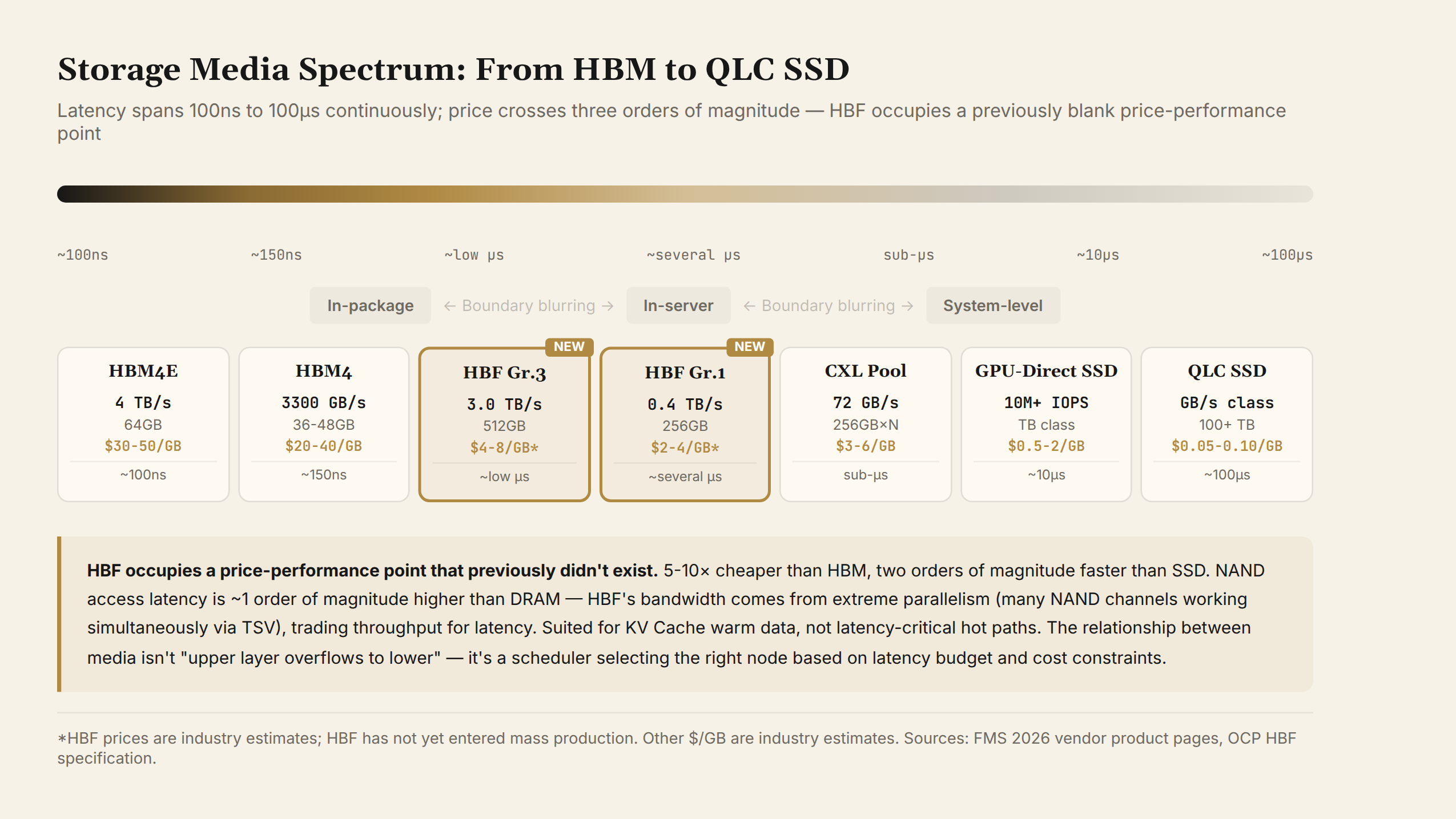
Viewing these media together:
| Medium | Interface | Bandwidth | Capacity | $/GB | Latency |
|---|---|---|---|---|---|
| HBM4E | In-package | 4 TB/s | 64GB | $30–50 | ~100ns |
| HBM4 | In-package | 3300 GB/s | 36–48GB | $20–40 | ~150ns |
| HBF Grade 3 | UCIe | 3.0 TB/s | 512GB | $4–8 (est.) | ~low μs |
| HBF Grade 1 | UCIe | 0.4 TB/s | 256GB | $2–4 (est.) | ~several μs |
| CXL Memory Pool | CXL 3.2 | 72 GB/s | 256GB×N | $3–6 (DDR5 + controller premium) | sub-μs |
| GPU-Direct SSD | PCIe 6.0 + SCADA | 10M+ IOPS | TB-scale | $0.5–2 | ~10μs |
| QLC SSD | PCIe 6.0 | GB/s-class | 100+ TB | $0.05–0.10 | ~100μs |
Latency spans from nanoseconds to hundreds of microseconds. Pricing spans three orders of magnitude, from $50/GB to $0.05/GB. The relationship between media is not "overflow from the upper layer to the next" — it's "the scheduler selects the optimal node based on latency budget and cost constraints." HBF fills the $2–8/GB zone that previously didn't exist, adding a new point on this spectrum.
IV. Protocol Evolution: Who Controls the Scheduling Interface
Physical connections and media nodes are in place. But who decides which medium a piece of data lives on? Who controls data movement? This is the protocol layer's contest.
FMS 2026 exposed three protocol lines intersecting.
cuFile + SCADA: GPU Takes Over Storage Scheduling
NVIDIA open-sourcing the cuFile API and launching the SCADA architecture is fundamentally about moving storage scheduling control from the OS kernel to the GPU side.
Traditional storage stack: application → system call → VFS → file system → block device layer → NVMe driver → SSD. This chain was designed around the assumption that the CPU drives I/O. SCADA truncates it: GPU → cuFile → SCADA → NVMe queue → SSD. The CPU is not in the path.
This isn't just performance optimization — it's an architectural power transfer. When the GPU manages NVMe queues directly, traditional file system semantics (open/read/write/close) are no longer the only data access method. The GPU can use more primitive interfaces to address storage locations directly — for KV Cache, a scenario that "doesn't need filenames, only key-value addressing," this strips away an unnecessary layer of abstraction.
NVIDIA simultaneously brought in Google, Intel, and Meta as founding maintainers, rallying 40+ storage vendors into the Storage-Next initiative. The core question: when the GPU replaces the CPU as the primary storage access initiator, how should SSDs adapt? The focus is optimizing 512-byte sector read/write performance — traditional SSD minimum management units (physical pages) have reached 8–16KB, while a single KV Cache access may be only 512 bytes. This means one effective 512-byte read moves 16–32KB of physical data, with read amplification exceeding 30×. Intel has joined the open-source organization and participates in code maintenance. cuFile and SCADA have been elevated from NVIDIA proprietary technology to industry-wide standards.
ICMSP: SSDs Gain Memory Semantics
If cuFile/SCADA changed how GPUs access SSDs, ICMSP changed how SSDs understand data.
A traditional SSD's FTL manages LBA (Logical Block Addressing) to physical page mapping. It neither knows nor cares what data sits in those blocks. ICMSP's specialized FTL brings KV Cache semantics into the storage layer: it knows which data belongs to the same attention head, which data belongs to the same prefix cache namespace, which data can be safely evicted.
This means the SSD transitions from "general-purpose block device" to "inference-dedicated memory node." Data organization shifts from "block sequences" to "KV tables + lifecycle tags." Addressing granularity shifts from 4KB to 512 bytes. Access patterns shift from "file reads/writes" to "memory addressing."
NVMe FDP: Industry-Standard Data Placement
While NVIDIA pushes cuFile/SCADA, standards bodies (the NVMe Working Group) are advancing FDP (Flexible Data Placement). FDP lets the host explicitly tag data placement and attributes — checkpoint data written to the SLC layer as burst buffer, hot data to the TLC layer for high-performance access, cold data sinks to the QLC layer.
FDP and cuFile operate at different layers — cuFile defines how the GPU initiates storage access; FDP defines how the SSD arranges data placement. They're complementary, not competitive. The real contest is this: NVIDIA wants cuFile to become the de facto standard for GPU-to-storage access (like CUDA for computing), while standards bodies want storage interfaces to remain vendor-neutral.
Core Judgment: Whoever Controls the Scheduling Interface Defines the Rules
The competition across three protocol lines points to one judgment: the center of value in storage architecture is shifting from the media layer (media is replaceable) to the scheduling layer (scheduling determines who has the most influence).
NVIDIA understands this. Its strategy: cuFile defines the GPU→SSD access standard, ICMSP defines KV Cache management semantics inside the SSD, the Storage-Next initiative defines industry specifications for next-generation storage devices. Three lines combined — NVIDIA is attempting to become the de facto standard-setter for the storage scheduling layer.
This is exactly the same strategy it executes in the compute layer with CUDA while observing UALink from the sidelines. Whoever controls the scheduling interface defines the rules — this judgment still holds.
V. Industry Fork: Three Routes in Contention
Assembling the signals, FMS 2026 reveals an industry-level fork: vendors have fundamental disagreements about the path to build storage architecture.
Samsung: The Closed Integration Route
Samsung simultaneously commands DRAM, NAND, wafer foundry, and advanced packaging — the industry's only IDM. Its route is end-to-end closed: zHBM (vertically stacked HBM) + zNAND-O (TSV NAND stacking) + V10 BV-NAND + HBM4E + LPDDR5X-PIM + enterprise SSDs, forming a proprietary full stack.
Strength: can deliver integrations no one else can (zHBM performance at 8× HBM5, density over 10×). Weakness: closed routes historically lose to open coalitions. zHBM is planned for 2029 mass production, 12–18 months behind HBF.
OCP / HBF Alliance: The Open Standards Route
Led by SK Hynix + Sandisk, published by OCP, with Google and Tenstorrent joining. The HBF standard went from inception to publication in 6 months — this is the speed advantage of open alliances.
Route logic: don't pursue proprietary integration; define open standards for multi-vendor participation. HBF uses a UCIe universal interface, NAND as the medium, OCP for ecosystem. Specs are conservative (Grade 1 tops out at 0.4 TB/s), but standardization-driven ecosystem momentum could overtake proprietary approaches over time.
NVIDIA: The Platform Coordination Route
NVIDIA doesn't manufacture media (no HBM, no NAND), but it defines the scheduling rules. cuFile + SCADA + ICMSP + Storage-Next initiative — NVIDIA's position in the storage scheduling layer mirrors its position in the compute layer with CUDA: no hardware, just rules.
Kioxia's GP1 featured in an NVIDIA keynote slot — a signal. The GPU-Direct SSD + ICMSP combination gives NVIDIA a complete vertical integration narrative from compute to storage. But it lacks DRAM capacity, lacks NAND capacity, and depends on partners.
Mirroring the Compute Industry
Samsung's closed integration ≈ Apple's vertical integration; OCP/HBF open standards ≈ the UALink coalition; NVIDIA's platform coordination = NVIDIA's own compute-layer strategy — control the scheduling interface, stay out of media manufacturing.
NVIDIA's storage strategy is more complex — it's hedging both sides simultaneously. cuFile/ICMSP is NVIDIA's own storage interface moat, with no direct relationship to the HBF Alliance. This means NVIDIA plays two roles in storage architecture: "rule-maker" (cuFile defining the GPU-SSD interface standard) and "ecosystem participant" (remaining independent outside the HBF Alliance).
On the China supply chain front, the FMS 2026 floor plan covered the full chain: YMTC (NAND IDM), DapuStor/Memblaze/Longsys (enterprise SSDs), InnoGrit/YEESTOR/Silicon Motion (SSD controllers), Montage Technology (CXL 3.2 controller trial production), ScaleFlux (computational storage + Gen6 + CXL across three lines), GigaDevice (storage chips). ByteDance appearing in the speaker list signals that Chinese CSPs are no longer just buyers — they're beginning to participate in storage technology direction discussions.
VI. NAND, Interfaces, and Checkpoint Engineering
The following signals are directionally important but represent incremental upgrades — consolidated here.
PCIe Gen6 SSD mass production begins. Kioxia CM10, ScaleFlux FC6116, and Kioxia GP1 are all Gen6 products. Controller competition accelerates: Marvell Bravera SC6, Silicon Motion MonTitan SM8466, and Phison PS5303-X3 all offer PCIe 6.0 solutions, with rated sequential reads reaching 28 GB/s (Marvell Bravera SC6, Silicon Motion SM8466). Gen7 has entered the agenda (CDFP X16 cables, PCIe L0p power analysis).
QLC Enterprise SSDs + Checkpoint Tiering. Kioxia displayed the LC9 245.76TB QLC NVMe SSD. Micron's 6600 ION reaches 245TB per drive; DapuStor's R6060 appeared at FMS 2026 in an E2 form factor at 512TB (up from the previous E3.L/E1.L maximum of 245TB). AI data centers need massive capacity for checkpoints, vector databases, and cold data — QLC is no longer just a "cheap consumer drive" label. After single-drive capacity breaks past 245TB, high-performance SSD controller power exceeds 45W, and onboard cold-plate liquid cooling in EDSFF (E1.S/E3.S) form factors has shifted from optional to industry standard.
The checkpoint scenario has produced a standard engineering pattern for SLC + QLC heterogeneous tiering:
- Burst Phase: When a checkpoint triggers, data writes at full speed to the SLC layer (or pSLC region within the SSD), letting GPUs quickly unfreeze and resume computation
- Destaging Phase: After GPUs resume training, background processes destage SLC data to the QLC layer via large-block sequential writes, with write amplification approaching 1.0, maximizing QLC endurance
- Recovery Phase: During failure recovery, checkpoints are read from the QLC layer — QLC read performance approaches TLC, enabling fast recovery
GPUs are too expensive — every additional minute of write time means thousands of GPUs burning electricity for nothing. SLC+QLC tiering has gone from "optional optimization" to "mandatory practice" at 10,000-GPU clusters.
VII. Predictions
Prediction 1: HBF Reaches Market Before zHBM
SK Hynix will deliver HBF Grade 1 products (8-layer stacking, ~0.4 TB/s, 256GB) in the second half of 2027, 12–18 months ahead of Samsung's zHBM mass production in 2029. The first-mover advantage of an open standard will attract more vendors to join the HBF Alliance. Validation window: Q3 2027.
Prediction 2: GPU-Direct SSD + ICMSP Enters NVIDIA Reference Designs in 2027
Kioxia GP1's NVIDIA keynote slot is a signal. ICMSP has already reduced TTFT by 82.7% — if NVIDIA includes GPU-Direct SSD as an optional memory expansion layer in its 2027 roadmap and builds ICMSP into the default inference framework, the architecture goes from "Kioxia + Solidigm exclusive" to "industry standard." Validation window: GTC 2027.
Prediction 3: CXL Memory Pools Face Structural Headwinds for Large-Scale Deployment
The CXL supply chain at FMS 2026 appears approaching deployment readiness — controllers in trial production, switch chips in mass production, memory modules in system validation. But from "supply chain ready" to "hyperscale CSP deploying CXL in production for AI workloads," several structural issues remain unanswered.
First, CPU vendor willingness. CXL liberates memory from CPU control into pooled resources, which weakens CPU platform lock-in. Intel and AMD have been half-hearted about CXL memory pooling — they support the protocol but aren't actively driving the ecosystem.
Second, software stack immaturity. OS support for CXL memory pool hot-plug, NUMA affinity, and page migration is still early. Large-scale production deployment requires deep kernel-level adaptation — it's not plug-and-play.
Third, NVIDIA doesn't push CXL. NVIDIA pushes ICMSP/SCADA (GPU manages storage directly), not CXL (CPU manages remote memory). In AI inference workloads, the GPU-direct-to-storage path is more dominant. CXL's sweet spot may be in traditional databases and virtualization, not AI inference.
A more pragmatic assessment: CXL memory pools may enter small-scale production validation in 2027 (a few CSPs for non-AI workloads), but "hyperscale CSPs大规模 using CXL for AI inference" still lacks sufficient structural drivers. Validation window: whether any CSP publishes CXL memory pool production data on AI workloads by end of 2027 — if not, it means this path is slower than the industry expects.
Open Questions
- HBF Alliance expansion: Will NVIDIA, AMD, or Meta join? If NVIDIA joins, HBF's ecosystem momentum hits a phase transition. But NVIDIA may choose not to join — preserving cuFile independence aligns better with its platform strategy than joining any storage standards coalition
- Scheduling software contest: The hardware exists, but OS and inference framework auto-tiering capabilities haven't caught up. NVIDIA's cuFile + ICMSP is racing to fill this position. Standards bodies (SNIA/NVMe) are also pushing data placement standards like NVMe FDP. Two lines competing: NVIDIA wants a closed platform; industry standards want open abstraction. This mirrors the CUDA vs. SYCL/OpenCL competitive structure exactly
Related Reading
- Inference Economics Part 3: KV Cache Scheduling Engineering discusses "what to do after compressing to 7%" — FMS 2026 delivers the hardware-layer answer: CXL memory pools and GPU-Direct SSDs for tiered management, with NVIDIA ICMSP turning SSDs into first-class KV Cache memory nodes
- Storage Supercycle: RAMageddon predicted AI inference would rewrite the storage hierarchy — FMS 2026 confirmed this judgment with the HBF standard and networked storage architecture. Storage chip growth revised from the spring forecast's 249.5% to 302%
- Inference Economics Part 1: Inference Pricing Teardown reverse-engineers inference pricing from physical cost — Micron's "memory is 50% of system value" means the primary variable in inference cost is shifting from GPU compute to memory and storage bandwidth
- Agent Storage Paradigm: Three Years of FMS Wind Shifts predicted KV Cache would become a cross-tier storage object and that Agents would generate random IOPS pressure — FMS 2026 validated both predictions directly with the GP1 (10 million IOPS, 512-byte granularity) and ICMSP
FMS changed its name. When a conference's very name can no longer contain what it discusses, the industry isn't going through a product cycle — it's undergoing an architecture rewrite. And the core of this rewrite is that the storage hierarchy is becoming a network — shareable, schedulable, and fundamentally different from the linear ladder we've lived with for forty years.
Disclosure: This article is based on the FMS 2026 official agenda and public coverage, Samsung/SK Hynix/Kioxia/Micron/NVIDIA official press releases and product pages, WSTS 2026 spring forecast and Q2 update, and the HBF specification document published by OCP. This is not investment advice. Data herein is current as of August 9, 2026.
Deutsche Bank research note following FMS 2026 meeting with Micron management (2026-08-06), citing Jeremy Werner, Senior Vice President of Data Center. ↩︎
WSTS (World Semiconductor Trade Statistics) spring 2026 forecast (June 2026); the August Q2 update revised the full-year forecast to $1.655 trillion, with memory chip growth further revised to 302%. ↩︎
Eastmoney report dated 2026-08-04 citing supply chain sources. ↩︎
NVIDIA/Solidigm/AIC joint announcement; figures are vendor-published results awaiting independent benchmark verification. ICMSP architecture details and the 82.7%/67% figures are from the FMS 2026 technical presentation slides; SCADA performance data is from the NVIDIA FMS 2026 keynote. No independent benchmark had been published as of writing. ↩︎ ↩︎ ↩︎
Samsung's official product page lists HBM4E specs (64GB/16H/4 TB/s/16 Gbps); sample shipment month not specified. Tonghuashun Finance reported on 2026-08-07 that SK Hynix delivered 12-layer HBM4E samples to customers in June. ↩︎
The GP1's 50 DWPD figure comes from vendor materials distributed during FMS 2026; Kioxia's official award press release does not list this parameter. ↩︎