
Specing an EDA cluster with an AI-cluster mindset is the most common mistake in enterprise EDA infrastructure planning today. Piling on cores, buying GPUs, deploying InfiniBand — these decisions usually stem from generic assumptions about compute infrastructure rather than any specific analysis of EDA verification workloads. The bottlenecks in EDA verification are fundamentally different from those in AI training. AI training is bounded by GPU interconnect bandwidth. EDA verification is bounded by memory bandwidth, storage I/O patterns, and the serial dependencies inherent in EDA tools. This article starts from the EDA workflow itself, identifies six categories of verification load that shape infrastructure decisions, derives hardware requirements from algorithmic first principles for each one, and delivers a heterogeneous cluster blueprint for a 30–40 node deployment.
EDA Workflow and Workload Identification
EDA (Electronic Design Automation) covers the entire flow from RTL code to tape-out. A chip design cycle typically runs 12–24 months, with EDA tools involved at every stage.
In the design phase, engineers write RTL code in hardware description languages (Verilog/VHDL) to define the chip's logical behavior. This phase is workstation-centric and places almost no demand on compute clusters.
Logic synthesis converts RTL into a gate-level netlist — Boolean logic gates and interconnects. Tools such as Design Compiler or Genus run at this stage with moderate compute requirements, typically handled on workstations or a small number of servers.
Physical design (Place & Route) maps the gate-level netlist onto a physical layout — deciding where each logic gate sits and how metal traces are routed. Tools such as Innovus and ICC2 run here, with single jobs lasting hours to over ten hours and memory requirements of 200–400 GB. This phase needs compute clusters, but parallelism is limited; the dominant pattern is large-memory single-node jobs.
Verification is the most compute-intensive part of the EDA flow and the primary driver of cluster scale. Verification is not a single operation — it spans multiple analysis types across functional and physical dimensions:
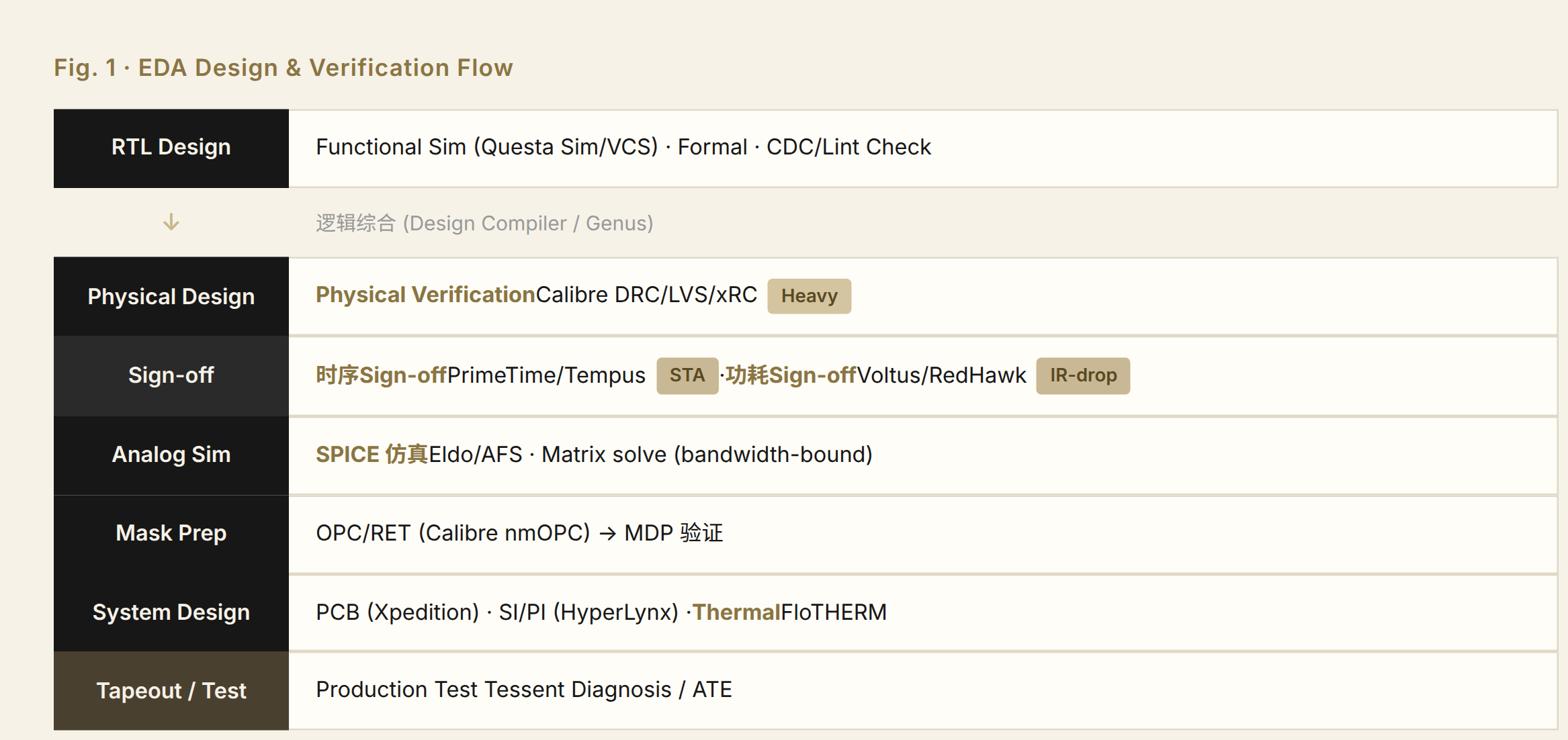
- Functional verification (digital simulation): Before tape-out, software simulates the chip running to verify correct logical behavior. Tools: Questa Sim, VCS, Xcelium.
- Analog circuit verification (SPICE simulation): Solves precise differential equations for analog circuits such as PLLs, ADCs/DACs, and SerDes. Tools: HSPICE, Eldo, AFS.
- Physical verification (DRC/LVS): Checks whether the layout complies with the foundry's manufacturing rules. Tools: Calibre, ICV.
- Static timing analysis (STA): Analyzes whether the chip can reach its target frequency across all process corners. Tools: PrimeTime, Tempus.
- Power integrity analysis (IR-drop): Analyzes the voltage-drop distribution across the power grid when the chip operates at full load. Tools: Voltus, Totem, RedHawk-SC.
- Thermal simulation: Analyzes the temperature distribution across the chip and package under operating conditions. Tools: FloTHERM, Icepak.
The compute demand of these six workload categories drives hardware investment. Other phases — design, synthesis, place and route — are either workstation-centric or manageable on single nodes and do not create cluster-level resource pressure. Not every company needs all six, however. The workload emphasis varies significantly by business type.
Foundries (TSMC, SMIC, Samsung Foundry). The core workloads are DRC/LVS and SPICE. A foundry performs sign-off-grade physical verification for every customer tape-out and also develops and maintains DRC rule decks — a 7 nm process rule set contains 5,000+ rules, and each process iteration requires a full regression run. The DRC cluster is typically the largest of all workload pools. For SPICE, the foundry must characterize standard cell libraries: tens of thousands of cells × 6–10 PVT (Process-Voltage-Temperature) corners, with delay, power, and noise metrics simulated individually for each cell — a massive compute load. IR-drop analysis supports sign-off power integrity for customer designs and reference power network design during process development. Digital simulation and STA are not primary foundry workloads — foundries do not design large-chip logic.
Fabless design companies (Nvidia, HiSilicon, MediaTek, Qualcomm). All six categories are in use, and each operates at cluster scale. Digital simulation is typically the largest: a single SoC project's regression suite of 300–500 test cases requires hundreds of concurrent runs, making simulation nodes the most numerous in the cluster. DRC/LVS demand surges before tape-out, with sign-off verification requiring large-memory nodes. STA runs continuously throughout the sign-off iteration cycle at high frequency. SPICE is used for analog IP (PHY, PLL, ADC/DAC). IR-drop and thermal simulation run during sign-off. Design-company clusters are typically heterogeneous, partitioned into workload-specific pools.
IP companies (ARM, Imagination, VeriSilicon). The core workloads are SPICE and digital simulation. ARM's primary business is designing and verifying CPU/GPU IP, which requires extensive SPICE characterization of standard cells and interface circuits, plus digital simulation to verify functional correctness. DRC/LVS is used for pre-delivery physical verification of IP, at moderate scale. STA and IR-drop serve IP sign-off. Digital simulation regression scale depends on IP complexity — a high-end CPU IP verification suite can rival that of a full SoC.
OSATs (ASE, JCET, TFME). EDA compute loads are light. The primary tools are thermal simulation (package-level) and limited IR-drop analysis (package power network). DRC, digital simulation, and STA are not involved — those are design-side activities. Compute needs are met with workstations and a few servers; building an EDA cluster is typically unnecessary.
EDA service providers (VeriSilicon,灿芯, Creative Electron). The workload profile depends on service scope. Turnkey design service providers have a workload profile close to that of a Fabless design company — all six categories in use. Providers focused on physical verification outsourcing run primarily DRC/LVS and need large-memory, many-core node pools.
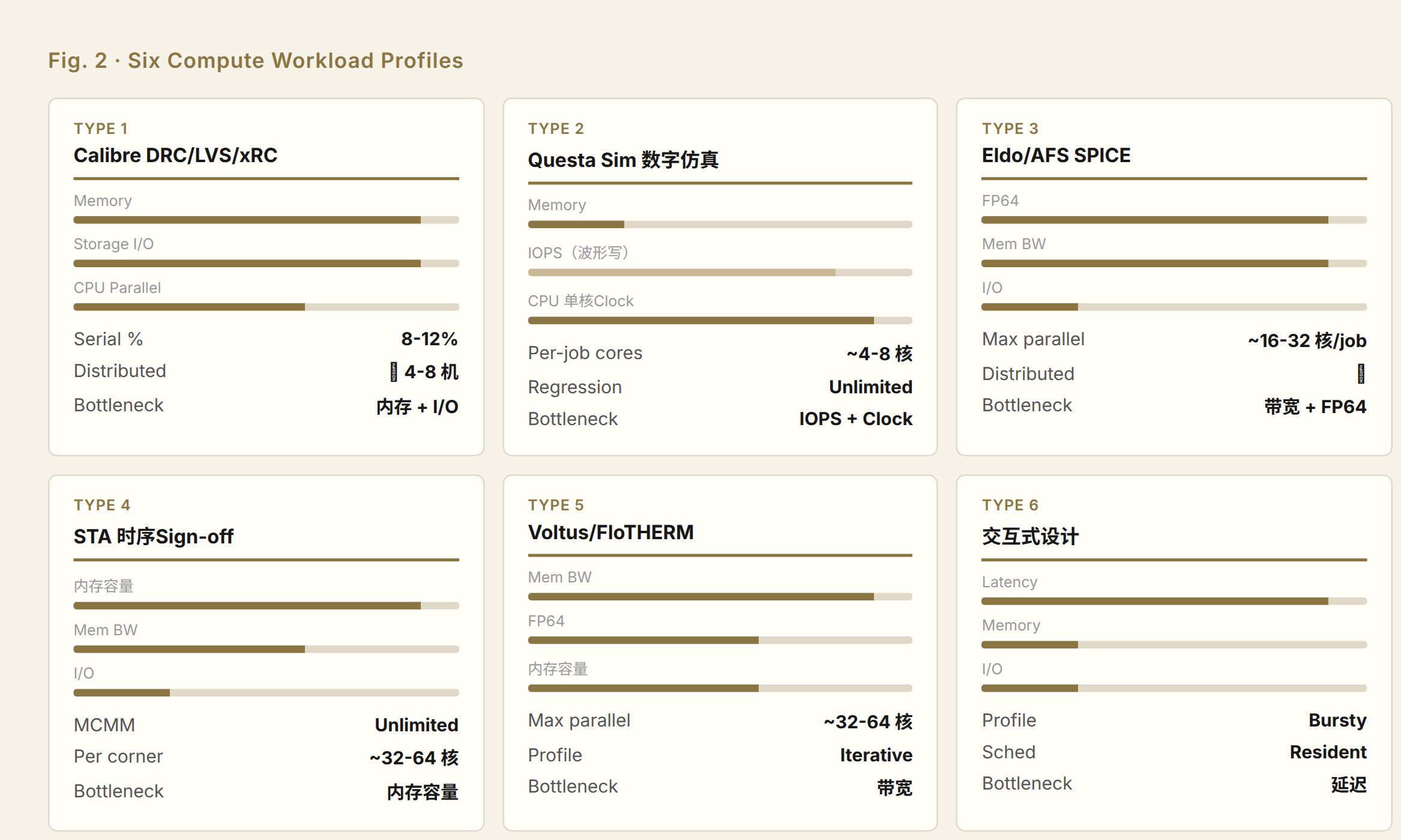
The target audience for the cluster blueprint in this article is organizations building a 30–40 node EDA cluster — primarily Fabless design companies and full-service EDA service providers. The following sections analyze each of the six workload categories from algorithmic principles to hardware requirements. Foundries and IP companies can select the relevant node types based on their own workload emphasis.
DRC: Geometric Operations and Hierarchical Traversal
Input: GDSII/OASIS layout file (50–200 GB for a 7 nm full-chip design), foundry-provided rule deck (5,000+ rules at 7 nm). Each rule is a geometric constraint — minimum width X nm, minimum spacing Y nm, via enclosure density ≥ Z%, metal density for a given layer between A% and B%.
Output: Violation report — each violation is a geometric region with coordinates, annotated with the rule it violates. A single full-chip DRC run typically produces 100,000 to 1,000,000 violations, each written as an individual small file (a few KB to tens of KB).
Computation: For every polygon in the layout, the tool executes computational geometry operations — Boolean operations (intersection, union, difference, for overlap checks), distance transforms (for minimum spacing checks), area and density statistics (for metal density rules), and polygon fracturing (decomposing complex polygons into trapezoids for scanline algorithm processing). A multi-billion-transistor SoC has on the order of a billion layout polygons, and each rule must be checked against all of them.
Compute pattern: Integer arithmetic and bitwise operations dominate. Layout coordinates use integer values (Database Units, typically 1 DBU = 0.1 nm). Geometric operations (intersection, union, difference, containment) are implemented via scanline algorithms on integer coordinates. There are no floating-point operations and no matrix solves. Compute intensity scales with polygon count × rule count — running a 5,000-rule deck on a full chip amounts to executing billions of polygon geometric operations.
Parallelism: The layout is partitioned by design hierarchy into sub-blocks, each checked independently (spatial parallelism). 64 blocks can be assigned to 64 CPU cores for simultaneous processing. However, at the boundaries between adjacent blocks, rule checks must wait for both sides to finish before merging results (barrier synchronization), which creates a serial bottleneck.
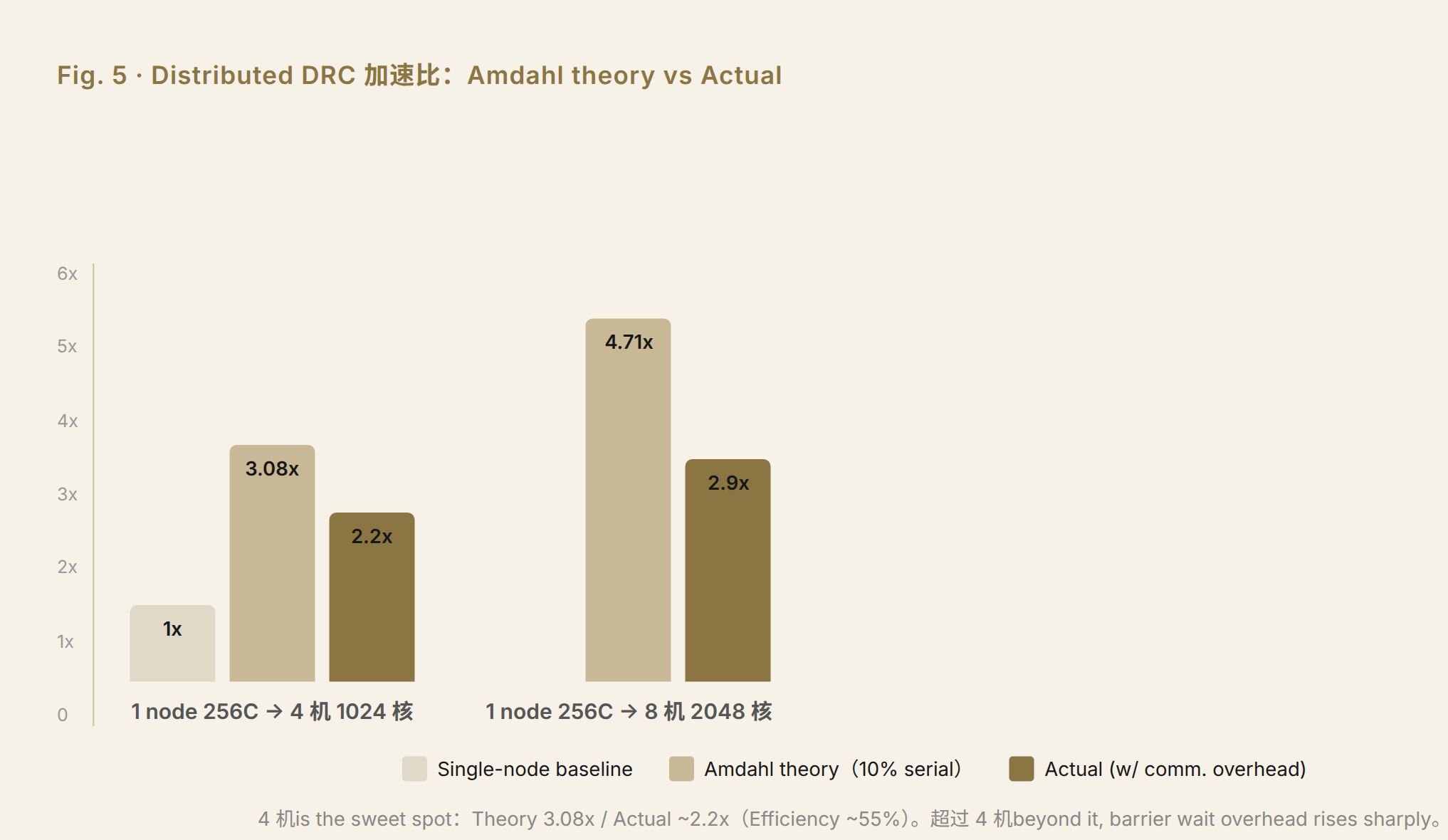
The serial fraction of full-chip DRC is approximately 8–12%. By Amdahl's Law, 10% serial overhead means that distributing across 4 machines yields a theoretical speedup ceiling of 3.08×, and roughly 2.2× after communication overhead. Beyond 4 machines, efficiency drops sharply — 4 machines is the efficiency inflection point; 8 machines drop to about 36% efficiency.
Hardware requirements: Loading a 200 GB layout requires large memory (7 nm full-chip working set: 600–900 GB). Multi-block parallelism benefits from many cores (128–256 cores show returns; beyond that, diminishing). Violation output is 100,000 to 1,000,000 small files of random writes, requiring 100,000+ IOPS. Layout file reads are large sequential reads, with a single job peaking at 3–5 GB/s. The read side needs bandwidth (large sequential files); the write side needs IOPS (small random files). Both must be served by the same storage system.
Digital Simulation: Discrete Event-Driven and Causally Serial
Input: Gate-level netlist or RTL code (tens of MB to several GB), testbench (describing the input signal sequence over time), timing annotation file (SDF — Standard Delay Format, specifying propagation delay for each logic gate).
Output: Waveform file (FSDB/VCD format, recording every signal's logic level at every time step — a single simulation run can produce tens of GB over hours), coverage report (functional coverage + code coverage, quantifying which logical paths were exercised).
Computation: Discrete event-driven simulation. The simulator maintains an event queue advanced by time step. At each time step, only gates whose inputs transition are processed: input values are read, outputs are computed via lookup or evaluation, and output changes are enqueued as new events. A single transition can trigger downstream gates, propagating an event chain. The simulation clock advances from t=0 to t=N, with each step strictly dependent on the previous one.
Compute pattern: Integer logic operations dominate — bitwise AND/OR/NOT/XOR, LUT (Lookup Table) lookups, comparisons, and branches. Signal values use four-state logic (0/1/X/Z, where X = unknown, Z = high-impedance). State computation is discrete logic — no floating-point, no matrix solves. Complexity scales with circuit size × simulation time × switching activity. A typical SoC simulation processes 1–10 million events per second.
Parallelism: The main simulation loop of a single run is strictly serial — each time step depends on the previous one, dictated by causality. Questa Sim's -mt multithreading provides only modest speedup on the testbench portion (about 1.2–1.5× with 2–4 threads); the main simulation loop is bounded at 4–8 cores. Regression testing, however, is fully independent parallelism: 300–500 test cases have zero inter-dependency and can run hundreds of vsim processes simultaneously. This is a textbook embarrassingly parallel problem — throughput scales linearly as long as CPU slots are available.
These two modes have radically different hardware needs. A single simulation run benefits from high clock frequency and strong single-core performance; more than 8 cores is wasted. Regression testing is throughput-oriented parallelism: a 64-core machine can run 16 concurrent 4-core jobs. Waveform writes are continuous small-file appends; at 200-way regression concurrency, the storage layer must sustain 150,000–200,000 write IOPS.
SPICE Simulation: Sparse Matrix LU Factorization
Input: Circuit netlist (SPICE deck, describing component values and connectivity, 10–500 MB), process model file (BSIM/CJM model parameters describing transistor nonlinear I-V characteristics), simulation directives (DC sweep, transient analysis, AC analysis).
Output: Waveform file (node voltages and branch currents over time), measurement report (scalar results: gain, bandwidth, phase margin, power). Unlike digital simulation waveforms, SPICE waveforms record continuous analog quantities with precision determined by the time step.
Computation: Transient analysis is SPICE's heaviest workload. At each time step: (1) Newton-Raphson iteration solves the nonlinear circuit equations (transistor I-V is exponential, requiring linearization and iterative convergence); (2) inside each Newton iteration, the linearized circuit is formulated as a linear system Ax = b and solved via sparse matrix LU factorization; (3) convergence is checked, and if not reached, the time step is reduced and the system is recomputed. Matrix A is the circuit admittance matrix with dimension equal to the number of circuit nodes; sparsity typically exceeds 99%.
Compute pattern: FP64 double-precision floating-point operations overwhelmingly dominate. LU factorization has O(n × k²) complexity (n = matrix dimension, k = average nonzeros per row), with FP64 multiply-add at its core. For a million-node circuit, a single LU factorization involves billions of floating-point operations, and memory reads/writes are 3–5× the compute volume — SPICE is a classic memory-bandwidth-bound application. The outer Newton-Raphson loop typically converges in 5–20 iterations, each requiring a full LU factorization.
Parallelism: Parallelism in LU factorization is constrained by the elimination tree structure. The root of the tree (trailing pivots) must complete before children can begin. Tree width determines available parallelism: small circuits (<100,000 nodes) top out at 8–16 threads; large post-layout circuits (>1,000,000 nodes) achieve near-linear scaling at 16 threads, with about 40% additional gain at 32 threads. The parallelism ceiling is set by the matrix dependency chain itself and cannot be broken by adding more cores. The right approach is to run 4 independent jobs concurrently on a 96-core node, each using 16–24 threads.
SPICE's I/O profile is "heavy at both ends, empty in the middle" — at start-up it reads the netlist and model files (10–500 MB), followed by hours to days of pure in-memory computation with almost no disk access, and finally writes out waveforms at completion. Storage pressure is the lowest among all six workload categories. Hardware priorities: FP64 throughput and memory bandwidth rank first and second; 16–32 threads per job is optimal; 512–576 GB memory covers most use cases.
STA: Longest Path on a Directed Acyclic Graph
Input: Gate-level netlist (millions of logic gates), timing library (.lib/.db — lookup tables for each cell's delay and transition time at every process corner), timing constraint file (SDC — defining clocks, I/O delays, false paths, multicycle paths), parasitic file (SPEF — RC network extracted from layout, where each wire segment is modeled as a resistor-capacitor pair).
Output: Timing report — for each path: start point, end point, delay value, and slack (positive = timing met, negative = timing violation). A single full-chip STA run produces hundreds of thousands to millions of path analysis results. The critical path — the path with the smallest slack — determines the chip's maximum operating frequency (Fmax).
Computation: The entire chip is modeled as a Directed Acyclic Graph (DAG) — each logic gate is a node, inter-gate connections are directed edges, and edge weights represent the RC delay of the interconnect plus the gate's intrinsic delay. Delay values are computed by looking up the timing library (NLDM/CCS/ECSM models), accounting for input transition time (slew) and output load capacitance. The tool then performs a longest-path search on the DAG to find the critical path that determines Fmax. Simultaneously, it performs setup checks (can data arrive before the clock edge?) and hold checks (does data arrive too quickly and corrupt the previous cycle?).
Compute pattern: Table lookup with interpolation and graph traversal dominate. Timing library lookup is 2-D table interpolation (input slew × output load), using linear or nonlinear interpolation. RC delay calculation uses the Elmore delay model or AWE (Asymptotic Waveform Evaluation) approximation — involving floating-point arithmetic but far less compute than SPICE matrix solves. DAG traversal has O(V+E) complexity (V = nodes, E = edges); traversing a million-node DAG is not inherently intensive, but each node's delay calculation involves repeated lookups and interpolation. Overall compute density is moderate, with mixed FP32/FP64 arithmetic.
Parallelism: Two dimensions. First, multi-corner multi-mode (MCMM) — each process corner (FF/TT/SS × different voltage and temperature combinations) is a fully independent analysis. 10 corners = 10 parallel processes, with no upper limit. Second, within a single corner, path analysis can be grouped by launch clock and parallelized, but group count is bounded by the number of clock domains — typically 16–32-way parallelism.
One characteristic that distinguishes STA from other workloads is invocation frequency: DRC runs a few times per day (each taking hours), while STA may run dozens to over a hundred times per day — an engineer fixes a timing violation and immediately reruns. This is the standard sign-off iteration loop. Hardware priorities: memory capacity ranks first (200–500 GB working set); 32–64 cores per corner shows returns; MCMM corners parallelize without limit.
IR-drop: Iterative Solution of Resistive Networks
Input: Layout power network (extracted from GDSII — power grid geometry), operating current distribution (per-node transient current waveforms from dynamic simulation or power analysis), package parasitics (resistance and inductance of bonding wires or bumps).
Output: Voltage drop map — IR-drop value at every point across the chip area (VDD supply voltage minus actual local voltage). Sign-off requires all points to be within tolerance (typically < 7–10% of VDD, i.e., 50–70 mV at 0.7 V). Current density distribution is also output for electromigration risk assessment.
Computation: The power grid is modeled as a large-scale resistive network (or RC network for transient analysis). VDD pads connect to the power supply; each transistor's supply pin is a current sink. The solution procedure: (1) build the nodal admittance matrix G (million to ten-million dimensional, extremely sparse); (2) inject the known operating current vector I; (3) solve G·V = I for node voltages. In transient analysis, this is solved at each time step with a time-varying current vector. For electromigration analysis, current density in each metal segment is back-computed from the voltage distribution and compared against process-defined current density limits.
Compute pattern: Sparse matrix iterative solve — Conjugate Gradient (CG) or GMRES, dominated by FP64 floating-point arithmetic. Matrix dimension is in the millions to tens of millions, with sparsity > 99.9%. The bottleneck in iterative solve is not raw floating-point count but Sparse Matrix-Vector multiplication (SpMV) — each iteration must traverse all non-zero matrix elements for multiply-add operations. Memory bandwidth is the bottleneck: the matrix data volume far exceeds the compute volume, and most time is spent waiting for data to travel from memory to registers. Typical convergence requires 100–1,000 iterations.
Parallelism: The SpMV within each iteration can be parallelized by spatial domain decomposition — partition the chip area into N sub-regions, compute each independently, and exchange data at boundaries. But iterations are strictly serial — iteration k+1 depends on iteration k. The parallel efficiency inflection point is 32–64 cores.
IR-drop is the second most memory-hungry workload in the cluster (300–800 GB working set), after DRC. Memory bandwidth is the number-one priority; 32–64 cores is the sweet spot.
Thermal Simulation: Numerical Solution of the Navier-Stokes Equations
Input: Chip physical model (dimensions, material thermal conductivity, heat capacity), package structure (substrate, solder, heat sink, TIM — Thermal Interface Material — thermal parameters), power distribution map (per-module power dissipation, typically exported from PrimeTime power analysis), boundary conditions (ambient temperature, convection heat transfer coefficient, cooling solution parameters).
Output: Temperature distribution field — steady-state or transient temperature at every grid point inside the chip and package. Sign-off requires the maximum temperature to stay within process/reliability limits (typically < 105–125°C). Thermal stress distribution and thermo-mechanical reliability risk points are also reported.
Computation: Solves the heat conduction equation (steady-state: ∇·(k∇T) + Q = 0) or the coupled thermal-convection equations (transient: including Navier-Stokes equations for fluid field and the energy equation for temperature field). The continuous domain is discretized into a mesh (FEM — Finite Element Method — or FVM — Finite Volume Method), a stiffness or coefficient matrix is assembled, and the solution is obtained via iterative solve for steady-state or time-stepped integration for transient.
Compute pattern: Like IR-drop, this is numerical solution of partial differential equations, dominated by FP64 sparse matrix operations. Thermal simulation adds a fluid dynamics dimension, however — if forced-air or liquid cooling flow fields must be analyzed, Navier-Stokes solution compute cost significantly exceeds pure heat conduction. Stiffness matrix dimension depends on mesh density, typically in the millions to tens of millions. Computation centers on SpMV and vector operations — memory-bandwidth-bound. The latest FloTHERM version supports GPU acceleration for select computations (mesh generation, matrix preconditioning), with returns varying by model size.
Parallelism: Time steps are serial (for transient analysis); within each step, parallelism follows spatial domain decomposition. The parallelism profile is similar to IR-drop, with 32–64 cores in the effective range. Memory requirement is approximately 200 GB — the lowest among the six workload categories.
CPU Side: Heterogeneous Node Pools
The six workload categories have distinctly different CPU requirements. DRC needs many cores (256) and large memory, dominated by integer geometric operations. Digital simulation single jobs need high clock frequency with few cores (4–8 cores), while regression testing demands massive concurrency — integer logic operations. SPICE needs FP64 throughput with high bandwidth and moderate core counts (16–32 threads per job) for dense matrix floating-point computation. STA needs large memory with moderate core counts, dominated by table lookups, interpolation, and graph traversal. IR-drop needs bandwidth with moderate core counts for sparse matrix iterative solve. Thermal simulation needs moderate core counts for PDE (Partial Differential Equation) numerical solution. No single CPU model covers all scenarios.
The reference platform is the Intel Xeon 6900P series (Granite Rapids-AP). The top SKU offers 128 cores per socket, 12 memory channels per socket, and supports DDR5-6400 RDIMM or MRDIMM-8800. Important caveat: the 6900P does not support DDR5-8000 RDIMM. Intel's July 2026 announcement of DDR5-8000 support covers only the 6700P (SP) series. For higher bandwidth on the 6900P (AP), the only option is MRDIMM-8800 (approximately 1,690 GB/s vs. approximately 1,229 GB/s for DDR5-6400).
A dual-socket system has 24 DIMM slots, and all must be populated. Every idle channel wastes bandwidth — 4 DIMMs use only 17% of available bandwidth, leaving CPU cores idle waiting for data. For bandwidth-sensitive workloads like DRC and SPICE, EDA tool vendor benchmarks and user field reports indicate performance losses of 30–60%.
The 6900P supports CXL 2.0. DRC nodes requiring more than 1.5 TB of local DRAM working set can consider CXL memory expanders. The trade-off is increased access latency (CXL memory adds ~30–50 ns vs. ~100 ns for local DRAM) and lower bandwidth than local DRAM. This makes CXL memory unsuitable for latency-sensitive workloads like SPICE, but practical for DRC's large working set scenario.
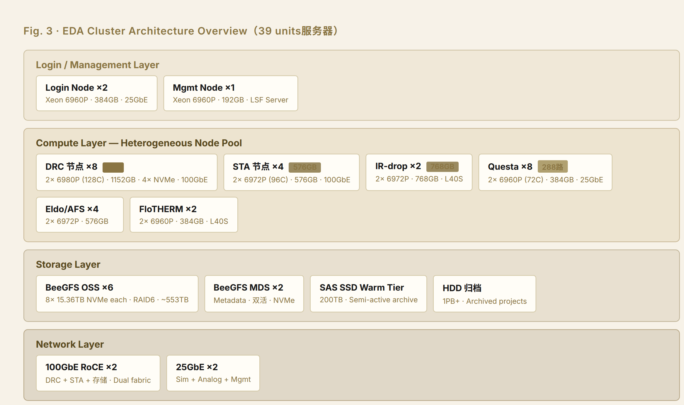
Configuration of the six node types:
- DRC node ×8: Dual-socket 128C (256 cores total), 1,152 GB (24 × 48 GB DDR5-6400), local 4 × 7.68 TB NVMe
- STA node ×4: Dual-socket 96C (192 cores total), 576 GB, 2 × 3.84 TB NVMe
- IR-drop node ×2: Dual-socket 96C (192 cores total), 768 GB, 2 × 3.84 TB NVMe, optional L40S GPU
- Simulation node ×8: Dual-socket 72C (144 cores total), 384 GB, 2 × 3.84 TB NVMe, 36 slots of 4 cores each = 288 concurrent jobs per node
- SPICE node ×4: Dual-socket 96C (192 cores total), 576 GB, 2 × 3.84 TB NVMe, 4–6 jobs per node × 16–32 threads each
- Thermal simulation node ×2: Dual-socket 72C (144 cores total), 384 GB, 2 × 3.84 TB NVMe, optional L40S GPU
Storage Side: Coexistence of Multiple Extreme I/O Patterns
The core challenge of EDA storage design is that a single system must simultaneously satisfy fundamentally different I/O patterns. DRC layout reads are 50–200 GB large-file sequential reads, peaking at 3–5 GB/s per job; 8 concurrent jobs demand 30–40 GB/s aggregate bandwidth. DRC violation writes are 100,000 to 1,000,000 small-file random writes at 100,000+ IOPS. Simulation waveform writes are 200-way concurrent small-file appends at 150,000–200,000 IOPS. SPICE mid-computation barely touches disk. STA reads timing libraries and parasitic files (several GB to tens of GB) and writes timing reports (moderate-size text files).
The solution is to route different I/O patterns through different paths.
Each compute node has 2–4 local NVMe SSDs (DRC nodes: 4 × 7.68 TB; others: 2 × 3.84 TB). DRC violation small files write directly to local NVMe (single drive: 1,000,000 IOPS). Simulation waveforms also write locally. After job completion, results sync to shared storage. In practice, DRC and simulation turnaround time improves by 30–50% — an 8-hour DRC run drops to 5–6 hours.
Shared storage uses an all-flash BeeGFS tier. 6 OSS (Object Storage Server) nodes × 8 × 15.36 TB NVMe per node, hardware RAID6 (6+2), yielding approximately 553 TB usable capacity with 40+ GB/s aggregate read bandwidth — serving shared reads for layouts, PDKs (Process Design Kits), and project directories. At the 20–40 node scale, BeeGFS is an order of magnitude simpler to deploy and operate than Lustre, with sufficient performance. Lustre is the right choice for 100+ node HPC centers.
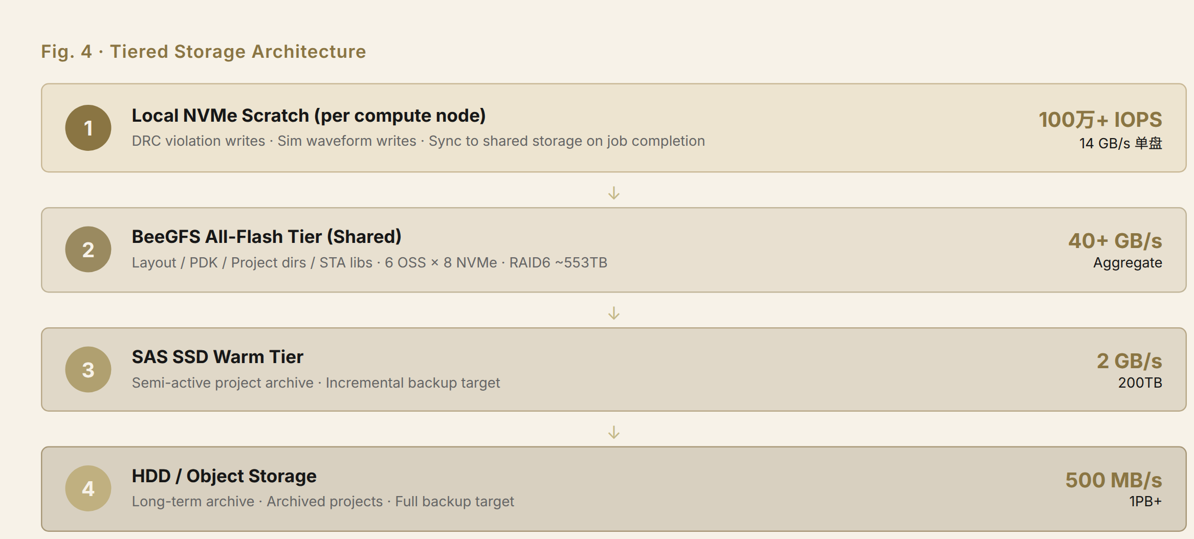
The Metadata Server must be deployed independently. EDA generates massive numbers of small files — 1,000,000 violation files means 1,000,000 file creation operations. If the metadata server is slow, file creation alone takes 10–30 minutes. This latency will not appear on any monitoring dashboard, but engineers will feel the DRC run "mysteriously slow down."
Network: 100GbE RoCE Is Sufficient
EDA distributed communication patterns are fundamentally different from AI. AI training uses AllReduce — thousands of GPUs exchange data continuously at high frequency with microsecond-level latency sensitivity. EDA distributed DRC uses barrier synchronization — 4 machines each compute their own block, wait for the slowest one, merge results, and proceed to the next round. This synchronization pattern has millisecond-level latency tolerance.
100GbE RoCE latency is 2–5 microseconds; InfiniBand is 0.5–1 microseconds. For millisecond-level barrier synchronization, there is no practical difference between the two. RoCE, however, is 30–50% cheaper than IB, simpler to operate, and compatible with the standard Ethernet ecosystem. In Phase 1 construction, purchase 100GbE switches outright — even if initial ports run at reduced speed, expansion later requires only new optical modules, not switch replacement or recabling.
Scheduling: Licenses Are the Hidden Bottleneck
The core principle of LSF (Platform Load Sharing Facility) scheduler configuration is queue separation by workload type. A DRC job requiring 1,152 GB of memory must have a dedicated node; a regression job needing 16 GB and 4 cores should share a 64-core machine with 15 others. Placing both job types in the same queue on a first-come-first-served basis leads to either OOM (Out of Memory) kills or 99% memory waste.
Licenses are a bottleneck in another dimension entirely. A single Calibre sign-off license can cost more per year than a DRC node. If licenses are not incorporated as a schedulable resource, one team can occupy all Calibre licenses for long-running jobs while other teams idle — hardware sits idle and license capacity is wasted. LSF License Scheduler can treat license features as schedulable resources: a job cannot start until its required license is available, and when licenses are exhausted, jobs queue for licenses rather than holding CPU slots. This single configuration change can deliver more practical impact than buying two additional servers.
Complete Blueprint
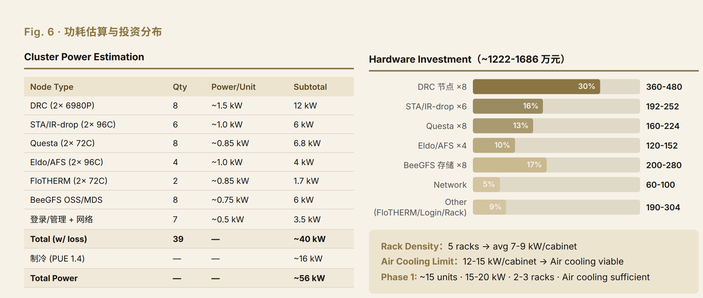
39 servers, 4 switches, 5 racks, total power draw approximately 56 kW (including cooling), hardware investment approximately 12.22–16.86 million CNY.
| Category | Node Type | Qty | CPU | Memory | NVMe | Network |
|---|---|---|---|---|---|---|
| Compute | DRC | 8 | 2× 6980P (128C) | 1152GB | 4× 7.68TB | 100GbE |
| Compute | STA | 4 | 2× 6972P (96C) | 576GB | 2× 3.84TB | 100GbE |
| Compute | IR-drop | 2 | 2× 6972P (96C) | 768GB | 2× 3.84TB | 25GbE |
| Compute | Questa | 8 | 2× 6960P (72C) | 384GB | 2× 3.84TB | 25GbE |
| Compute | Eldo/AFS | 4 | 2× 6972P (96C) | 576GB | 2× 3.84TB | 25GbE |
| Compute | FloTHERM | 2 | 2× 6960P (72C) | 384GB | 2× 3.84TB | 25GbE |
| Management | Login | 2 | 2× 6960P | 384GB | 2× 960GB | 25GbE |
| Management | Admin | 1 | 1× 6960P | 192GB | 2× 960GB | 25GbE |
| Storage | BeeGFS OSS | 6 | 1× 6960P | 384GB | 8× 15.36TB | 100GbE |
| Storage | BeeGFS MDS | 2 | 1× 6960P | 192GB | 4× 3.84TB | 100GbE |
A two-phase deployment is recommended. Phase 1 spends 5–7 million CNY on the following 15 nodes: 4 DRC nodes + 2 STA nodes + 4 simulation nodes + 2 SPICE nodes + 1 shared IR-drop/thermal node + 2 login/management nodes. Storage side: 3 OSS + 1 MDS. After 3 months of operation, LSF accounting logs provide precise bottleneck data (CPU, memory, storage, or license). Phase 2 then targets expansion to the full blueprint based on measured data.
Estimated per-node system power draw: DRC node approximately 1.6 kW (dual-socket CPU TDP 700 W + 24 DIMM ~150 W + 4 NVMe ~40 W + motherboard/NIC/fans ~200 W). Simulation/SPICE/STA nodes approximately 1.0–1.2 kW. Storage OSS node approximately 1.4 kW. Total IT power draw for 39 nodes is approximately 45 kW; at PUE 1.3–1.4, total facility power is approximately 58–63 kW (including cooling).
How EDA Clusters Differ from AI Clusters
AI training partitions a single model across thousands of GPUs, with AllReduce communication between nodes at microsecond-level latency sensitivity, requiring InfiniBand 200–400G. The core schedulable resource is GPUs. EDA assigns large numbers of independent tasks to matching node pools, with barrier synchronization between nodes at millisecond-level tolerance — 100GbE RoCE is sufficient. The core schedulable resources are CPUs and licenses. AI's bottleneck is GPU count and interconnect bandwidth. EDA's bottleneck is memory bandwidth, storage I/O, and license count.
Configuring an EDA cluster with an AI mindset — buying GPUs, deploying IB, stacking homogeneous nodes — creates a fundamental mismatch between resource allocation and actual workloads. For an EDA cluster, three measures deliver more impact than buying 10 additional servers: populate all 24 DDR5 channels, write local NVMe scratch locally, and incorporate licenses into the scheduler.
Data sources: Intel Ark 6980P/6960P official specification pages; Intel 2026-07-21 DDR5-8000 RDIMM announcement (verified via three sources: ITHome, Pacific Computer Network, Donews). Not a purchase recommendation. Data current as of 2026-07-28.