
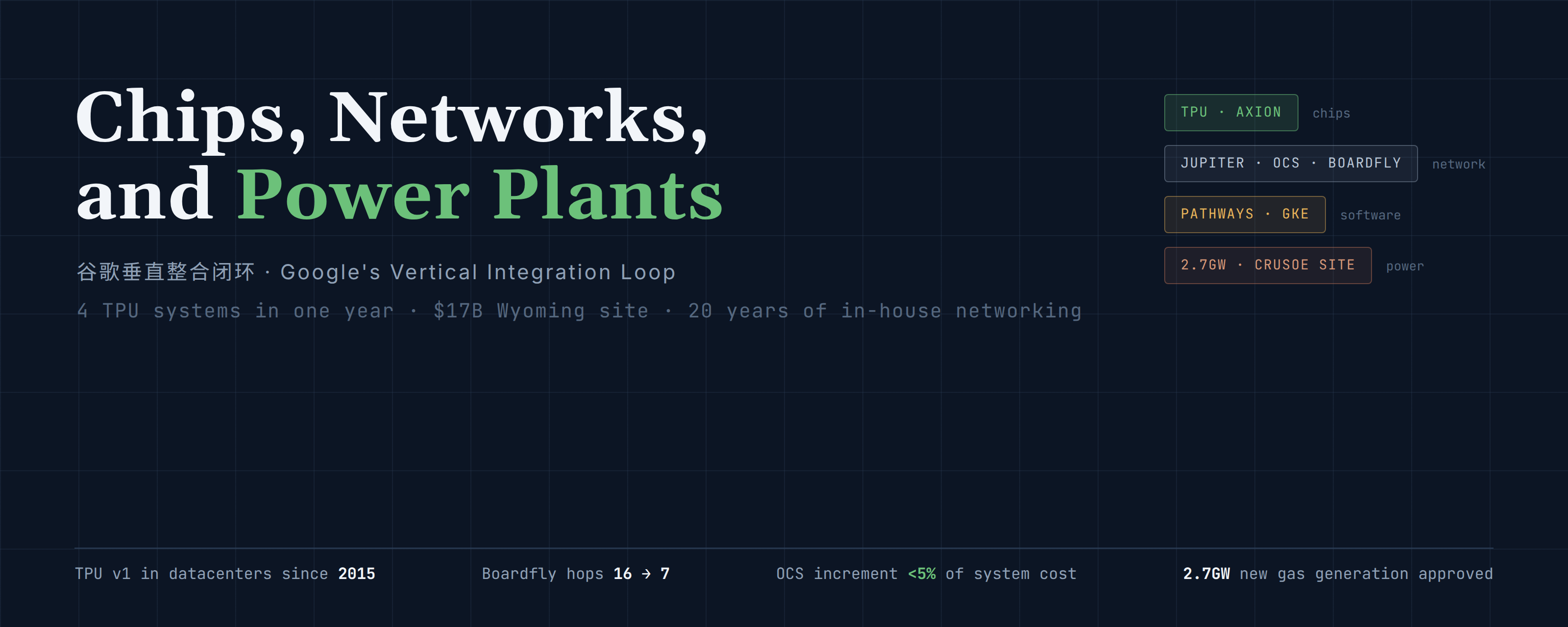
The bottleneck of AI compute is shifting from chips to power. Within one week, Google launched two new TPU systems and bought a data center site in Wyoming. Behind the four TPU systems released this year sit only two silicon designs; the self-developed data center network has been evolving for two decades, from the first-generation Firehose in 2005; the Crusoe deal brings power and land inside the operating radius. This article takes the vertical-integration route apart across four layers — chips, network, software, and power — and marks what it is made of and where its boundaries run.
While most companies still worry about GPU supply and bandwidth, Google did two things within a single week: it launched two new TPU systems, which did not require a fresh tape-out but recombined existing chips; and it bought a data center site, bringing power and land inside the operating radius. Add a self-developed data center network that has been running for two decades, and Google's route looks nothing like "swap in a bigger switch": it holds the compute stack's principal layers in its own hands.
In early November 2026, Google made three moves in a row. On November 5, it announced a $17 billion investment to build its first Wyoming data center. The next day, it bought the entire site from the developer, Crusoe. On November 9, it released the third and fourth systems of its eighth-generation TPU: the TPU 8tx for confidential computing, and the TPU 8i Max, which packages two inference chips into one package. Only seven months had passed since the 8t and 8i shipped in April. The three moves point to one question: where does compute come from?
The network wall study we covered this week — the Turbalance–LBNL high-radix switch simulation — represents one answer: build a switch chip with ten times the radix and flatten the multi-tier network into a single hop. Google's answer is the other one: design its own chips, evolve its own network for twenty years, and start holding its own power and land. The two routes overlap in the problems they attack; in method they barely intersect.
This article takes the route apart by layer: the combinatorics of the chip layer, the timeline of the network layer, the scheduling of the software layer, and the deal structure of the power layer. Each layer has public specifications and papers behind it; parts Google has not disclosed are marked as such.
1. The Chip Layer: Four Systems in One Year, Not Four Chips
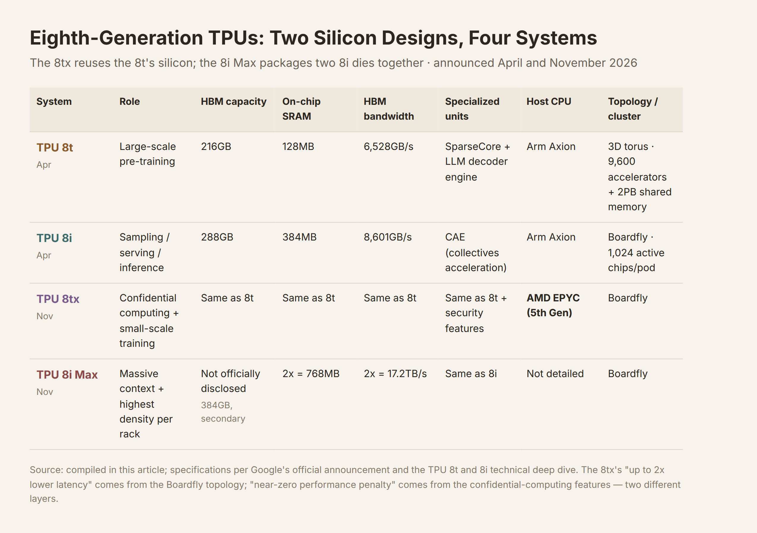
The eighth-generation TPU now has four systems, but only two silicon designs behind them.
- TPU 8t (released in April) targets large-scale pre-training: 216GB HBM, 128MB of on-chip SRAM per chip, 6,528GB/s of memory bandwidth. A single superpod connects 9,600 accelerators sharing 2PB of high-bandwidth memory.
- TPU 8i (released the same month) targets inference: 288GB HBM, 384MB of on-chip SRAM (three times the 8t's), 8,601GB/s of bandwidth. A pod has up to 1,024 active chips, with 1,152 physically installed; the purpose of the difference is not officially explained.
November's two new systems build on those two designs: the 8tx reuses the 8t's silicon, and the 8i Max packages two 8i chips together.
The value of this approach is speed of response, and the confidence behind that speed is a decade of accumulation.
The first TPU entered Google's data centers in 2015. The ISCA 2017 paper laid out the full accounting: a systolic array of 65,536 8-bit MACs, 92 TOPS of peak throughput, and 28MiB of software-managed on-chip memory. Against contemporary CPUs and GPUs it delivered 15–30x the performance and 30–80x the performance-per-watt. That paper was later named one of ISCA's most influential papers across twenty-five years.
The second generation had a rougher ride. The TPU v2 paper was rejected by ASPLOS, and a revision covering v3 was rejected by ISCA. The reviewers' verdicts: "no new ideas," and "it couldn't be research since it was already built" (as Jouppi recounts in his ISCA fiftieth-anniversary retrospective). The paper eventually found its home in the Communications of the ACM (2020). Those rejections also led directly to ISCA's industry track, where the TPU v4 paper was later published. Engineering running ahead of the academic review system is itself a footnote to the accelerator age.
By the eighth generation, two silicon designs support four systems, and the compounding starts to show. When confidential computing demand arrived, Google did not tape out a new chip. It paired the 8t's silicon with host CPUs carrying hardware-level security features, swapped the training-optimized torus for the Boardfly network introduced with the 8i, and the 8tx existed.
The official claim needs to be taken apart. Up to 2x lower latency than the 8t — that comes from the network topology. A near-zero performance penalty for confidential computing itself — that comes from the hardware security features. The two numbers belong to different layers; the announcement puts them in one sentence, which is easy to misread.
The 8i Max addresses a different problem: the memory wall. When dozens of agents work over one codebase or hours of video, memory bandwidth tops out before compute does. Google packages two 8i dies into one package, and the official confirmation covers three things: double the compute, double the on-chip SRAM, and double the HBM bandwidth.
Memory capacity was not given in the announcement; third-party reporting puts it at 384GB, about 1.33x the 8i's. If that number holds, one asymmetry is worth noting: capacity goes up 1.33x while compute goes up 2x, so KV cache per unit of compute is actually lower than on the 8i. Google also emphasizes that fitting twice the silicon into the existing rack footprint raises compute density per square foot and per watt — but it does not disclose the corresponding power and thermal numbers. The hidden cost of density can be seen to exist, not sized.
Specialization goes deeper. The 8t carries two purpose-built pieces: the SparseCore for embeddings, and an LLM decoder engine. The 8i's CAE (Collectives Acceleration Engine) accelerates the reduction and synchronization steps of autoregressive decoding and chain-of-thought inference; the previous-generation Ironwood put four SparseCores in that spot. The divide between training and inference is written into the die structure itself, not left to the same chip running different workloads.
One more number shows how Google defines "good." Among the 8t's official metrics is goodput per watt: not peak FLOPS, but effective throughput after failures and recovery, divided by power. For the company running the world's largest fleet of self-used AI workloads, that metric tracks real cost better than peak numbers.
2. The Network Layer: Twenty Years of Evolution, Not One Bet
The network is the deepest layer of Google's vertical integration, and the most commonly misread. The popular story is "Google replaced its switches with optical circuit switches." The actual record is a twenty-year evolutionary chain: the first generation of Google's in-house data center network, Firehose, began in 2005 (Jupiter Rising, SIGCOMM 2015), and Watchtower, Saturn, and Jupiter followed one another, with the OCS's role shifting along the way.
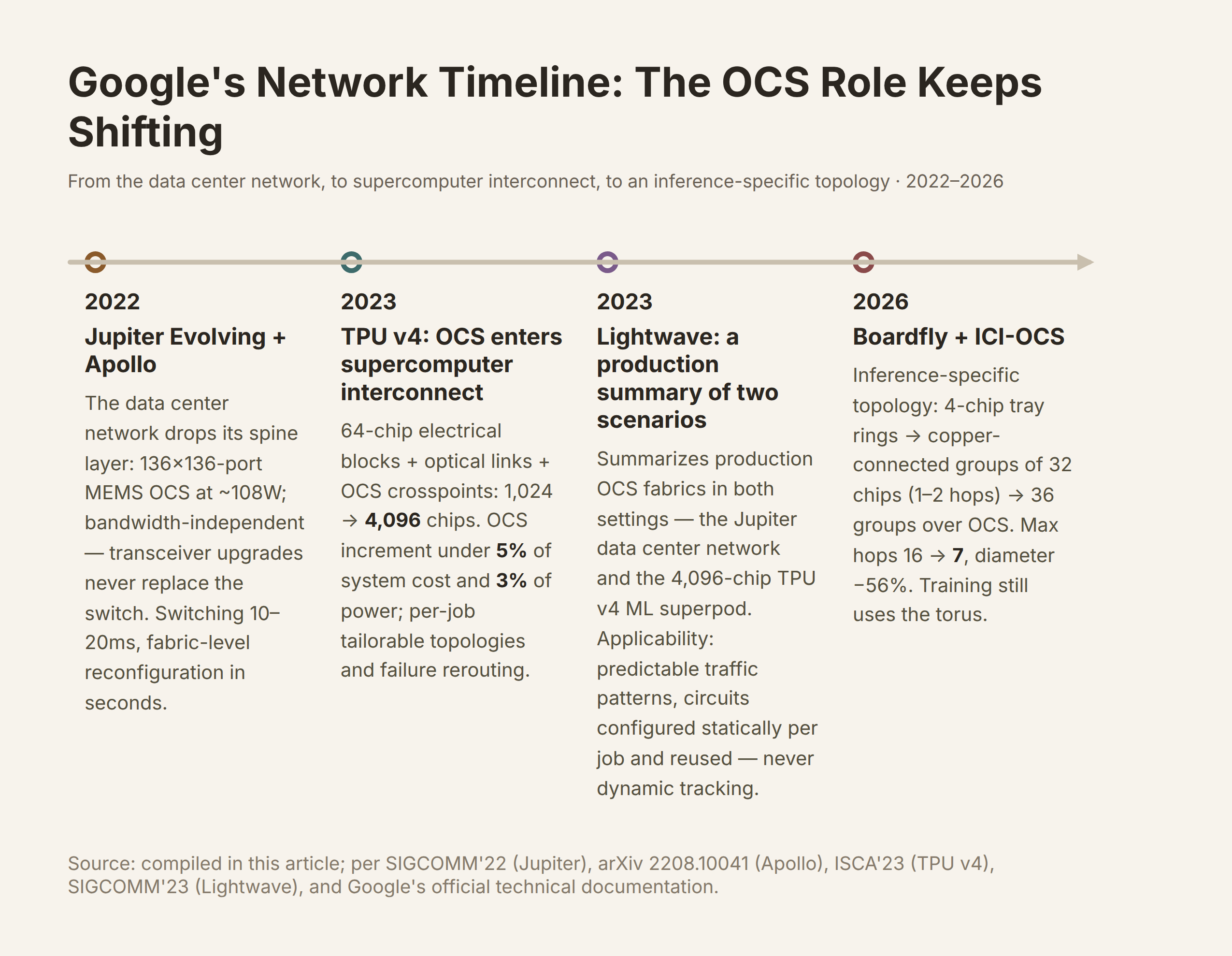
Apollo and Jupiter (2022 paper, deployed earlier): OCS enters the data center network. Google's SIGCOMM 2022 paper covered Jupiter's evolution, and in August 2022 the full Apollo OCS design appeared on arXiv. Apollo is a home-grown 136×136-port non-blocking OCS based on MEMS mirrors, drawing about 108W against the roughly 3,000W of an equivalent-port electrical switch. Its most counterintuitive property is bandwidth independence: it switches light paths, not packets, so when transceivers move to higher rates, the switch itself does not change. The cost is speed: commercial OCS switching time is 10–20 milliseconds, with fabric-level reconfiguration in seconds. Jupiter's architecture compressed the conventional multi-tier CLOS spine into direct block-to-block links plus one layer of OCS reconfiguration.
TPU v4 (2023): OCS enters supercomputer interconnect. The ISCA 2023 TPU v4 paper gives the full accounting. Sixty-four chips form an electrically interconnected building block, blocks link over optical fiber, and the OCS sits at the crosspoints providing reconfiguration, scaling the system from 1,024 chips in the previous generation to 4,096. The OCS increment costs under 5% of system cost and under 3% of power. Reconfiguration buys two things: topologies tailored per job, and fast rerouting after failures. That accounting is the quantified evidence for "cheap elasticity."
Lightwave (2023): a production summary of two scenarios. The Lightwave Fabrics paper from the same year summarized production deployments of optical-circuit-switch fabrics in both settings — the Jupiter data center network and the TPU v4 ML superpod, the latter spanning 4,096 chips. The paper is honest about applicability: lightwave fabrics pay off for "long-lived traffic patterns" and "predictable traffic patterns in tightly-coupled ML clusters." In other words, training communication patterns are largely known before the job starts, circuits can be configured statically per job and reused for the job's life, and millisecond-scale dynamic switching is never required.
Boardfly and ICI-OCS (2026): the topology redesigned for inference. By the eighth generation, training and inference use different networks. The 8t keeps the training-optimized 3D torus; the 8i introduced the Boardfly topology. The official technical documentation describes it in three layers:
- Bottom: each four-chip tray connects its chips into a ring over the inter-chip interconnect (ICI), leaving 16 external links; 11 of them serve the intra-group copper connections, and the rest rise to the optical layer.
- Middle: eight trays are fully connected with copper cabling into a group of 32 chips, any pair one to two hops apart.
- Top: 36 groups link through Apollo OCS into a single memory and compute space per pod.
Against a 3D torus of similar capacity, the maximum hop count drops from 16 to 7 and network diameter shrinks 56%, which Google says translates directly into lower tail latency; per the Google account relayed by Next Platform, average inference latency falls 50%. The topology's lineage runs back to the dragonfly family long used in supercomputing. Readers of the network wall piece may recall that LBNL's Michelogiannakis co-authored Dragonfly+; flat topologies have been this field's academic mainline for over a decade.
Put together, Google's networking philosophy is per-scenario tool choice, not one technology fits all. Training traffic is predictable, so OCS configures statically per job. Inference is latency-sensitive, so the near topology compresses to one hop of copper. Meanwhile, Next Platform's reporting notes a fact that is easy to miss: OCS is more expensive and rarer than Ethernet switches built on Broadcom, Cisco, or Nvidia silicon, and Google uses them on the training side only when it must. Optical circuit switching is not Google's religion; it is a class of tool used in specific positions.
3. The Software Layer: The Other Half of the Loop
The November 9 announcement is, by word count, nearly forty percent software. The section title deserves verbatim quotation: "Building the computer around the chip." Hardware differentiation is cashed in by software, and three components are worth unfolding.
TPU Sync. It unifies HBM, host DRAM, shared storage, and the data center network into one tiered KV cache system, with the official claim of a 90%+ reduction in time-to-first-token. This maps directly onto the 8i's hardware: the 384MB of on-chip SRAM holds the most active KV (our inference; the official material does not state this use), and what does not fit cascades down through HBM, host memory, and further tiers. The SRAM configuration on the chip and the tiered cache across the network are two faces of one design.
GKE dynamic slicing. It uses the OCS's reconfiguration capability for resource scheduling at the topology layer: TPU cubes are sliced into super-slices or sub-slices per job, and failures are recovered by rewiring circuits. The official numbers are job startup up to 5x faster and failure recovery up to 4.5x faster. This is the production-grade cashing-in of the claim above: OCS elasticity is spent at the topology layer. Slicing and recovery operate at second-to-minute scales, for which the OCS's 10–20 millisecond switching time is ample.
Cloud Pathways. The DeepMind runtime behind Gemini's training is now open to all cloud customers through GKE, with a single-controller architecture: pathwaysutils orchestrates multiple TPU slices as one local machine. It supports cross-slice pre-training, reinforcement learning, and multi-host inference; jobs survive hardware disruption, with sub-minute hot-swapping and elastic resharding. The massive-context workloads the 8i Max serves have cross-slice orchestration as their software precondition.
Openness is also shifting. TorchTPU is open source with vLLM and SGLang backends, and the XLA Serving Engine is open source alongside it. Combined with the customer-datacenter deployments discussed below, Google is actively loosening the old impression that "TPU is for Google only."
4. Power and Land: From Renting to Buying
The Crusoe timeline deserves a full retelling:
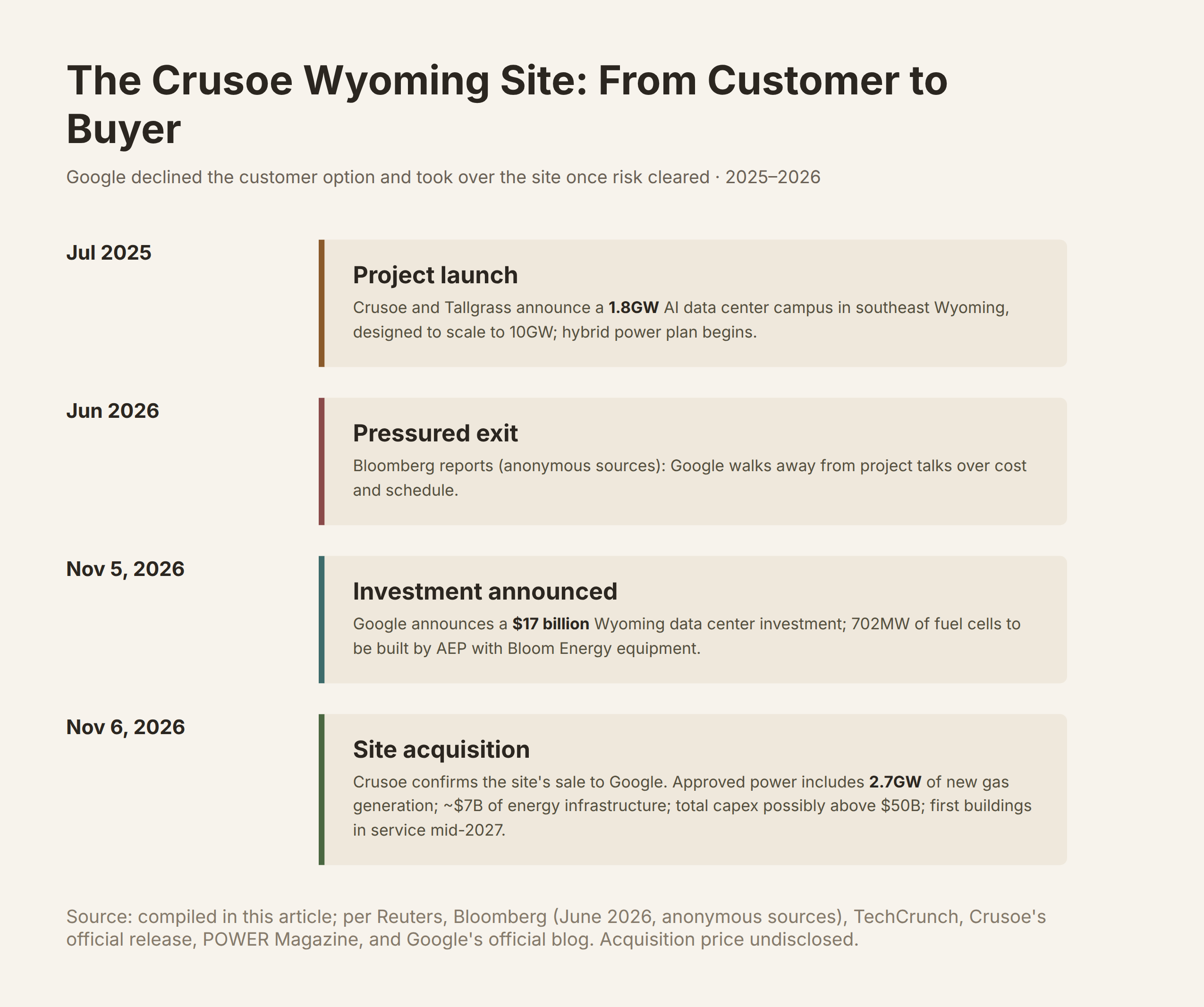
- July 2025: Crusoe and the energy infrastructure company Tallgrass announced a 1.8GW AI data center campus in southeast Wyoming, designed to scale to 10GW.
- June 2026: Bloomberg reported on anonymous sources (with TechCrunch following) that Google had pushed out of the project over cost and schedule.
- November 5: Google announced its $17 billion Wyoming investment.
- November 6: Crusoe confirmed the sale of the entire site to Google.
The structure of the deal is more informative than its headline number. Google declined the customer option and chose to take over the whole site after the developer had cleared the riskiest early work — siting, permitting, and the power plan.
The power plan is the core asset. It is a hybrid architecture of fuel cells, grid power, and gas turbines, with long-term plans to tie into Tallgrass's regional carbon capture hub. Per POWER Magazine, the approved campus includes 2.7GW of new gas-fired generation and about $7 billion of energy infrastructure. Tallgrass's project director estimates total project capex could exceed $50 billion, with the first buildings in service by mid-2027. Google's same-week blog disclosed 702MW of fuel cells built by AEP with Bloom Energy equipment.
Note that the $17 billion should not be read as the budget for those power facilities; its composition is undisclosed. What can be confirmed is that in what Google bought, power and land weigh no less than the buildings themselves.
Crusoe is not the loser. It holds more than 6GW of contracted capacity and a 40GW+ pipeline, and is developing another campus for Google in Armstrong, Texas. The division of labor this deal displays may be the coming norm: developers carry early risk for development returns; hyperscalers hold assets once risk clears. When power, not chips, becomes the binding constraint on expansion, the radius of vertical integration extends from the machine hall to the power plant gate.
5. Comparison: Full Stack, Rack-Scale, and Single-Point Silicon
Placed in industry coordinates, three models separate cleanly.
- Rack-scale systems (Nvidia): NVLink fabric, the CUDA ecosystem, and reference designs, but manufacturing rides on foundries, and data centers and power ride on partners and customers.
- Single-point designs (Meta's MTIA, Microsoft's Maia, Amazon's Trainium): replacing the accelerator layer on commercial infrastructure.
- Full stack (Google): as far as public information goes, Google is the only company with a public record across the full chain — chips, a self-developed data center network fabric (OCS included), scheduling software, self-built data centers, and power purchasing. The host CPUs of both the 8t and the 8i are Google's own Axion rather than x86 (the 8tx is the exception, see below); even that layer is in-house.
The supply-chain signal is just as telling. Per Chosunbiz, Google's HBM purchasing is now on par with Nvidia's, with per-chip HBM climbing from Ironwood's 192GB to the 8t's 216GB and the 8i's 288GB. Designing its own chips has not taken Google out of the supply chain competition; it has made Google a supply-chain buyer of Nvidia's magnitude.
The loop's boundaries are equally clear. First, the 8tx's host CPU is AMD's fifth-generation EPYC, not Google's own Axion: confidential computing needs a mature security-hardware ecosystem, and Google chose to buy rather than build. Second, HBM is entirely purchased. Third, manufacturing is outsourced. "Everything in-house" was never the fact. The accurate statement is: use the ecosystem where mature parts solve the problem faster, and build where the differentiation pays.
6. Boundaries and Critique
OCS elasticity lives at the topology layer, not inside the training step. The network wall piece covered MoE training's hundreds of All-to-All collectives per step; that conclusion is used directly here. Optical circuit switching times are 10–20 milliseconds, fabric-level reconfiguration runs in seconds, and the traffic matrix inside a training step changes on millisecond scales. Google's own Lightwave paper says it plainly: OCS serves ML clusters on the strength of predictable patterns and statically configured, long-lived circuits, not dynamic tracking.
So the real division of labor between the routes is this. The Eridu route (Eridu is the high-radix switch-chip company profiled in the network wall piece) absorbs communication dynamism inside the step with a packet-switched single-hop fabric. Google's route gives step-level communication to dedicated ICI (torus or Boardfly) and spends OCS only where it is strong: topology-layer elasticity, slicing, and cost. OCS did not remove the bandwidth wall; it props up the wall more cheaply and at lower power. The 8tx's "up to 2x lower latency" comes from Boardfly shortening paths, not from OCS doing low-latency switching.
A roadmap with home-team priority built in. The official line says the TPU business serves nearly a hundred customers, that customers can deploy TPUs into their own data centers, and that TorchTPU is open source. The old "walled" label needs updating. But a different asymmetry remains real: the four-system cadence is defined by Gemini's internal demand; external customers' configurations and delivery priority follow internal scheduling; and non-merchant silicon has no third-party OEM ecosystem. It is not a wall but a set of concentric circles: the closer to the center, the earlier the new systems arrive.
The hidden cost of density. If the 384GB figure holds, the 8i Max's capacity-versus-compute asymmetry shows that density is not free: the power and thermals of doubled silicon in one package are undisclosed. If performance-per-watt gains come at the cost of KV capacity per FLOP, the trade is not obviously net-positive for KV-heavy workloads. For now the judgment stays at "the problem exists; the magnitude is unknown."
Power binds before chips. The evidence is not the investment breakdown (undisclosed) but the deal structure itself: Google paid a whole-site acquisition price for a campus not yet built, and the main components of what it bought were a power plan and land. Chips can be reordered; grid interconnection queues are measured in years.
Watchpoints
- The actual pace of TPU deployments into customer data centers. The official line has opened the door; the first publicly disclosed third-party deployment would expand the concentric circles another ring.
- The 8t's training-side scale-out network. It remains undisclosed. If the next training pod also picks up OCS or a new flat topology, Boardfly's route is flowing from inference back into training.
- Whether the Crusoe pattern becomes standard — developer de-risks, hyperscaler takes over. The next test case is whether the Armstrong campus repeats the Wyoming path.
- The OCS cost curve. It is today's expensive, rare component, and the only bandwidth-independent layer in Google's network; if commercial OCS (the nEye and Salience line) brings prices down, the key constraint on this architecture loosens.
Sources
- Google official blog: Introducing TPU 8tx and TPU 8i Max (November 9, 2026); Wyoming data center investment announcement (November 5, 2026)
- Google Cloud: TPU 8t and TPU 8i technical deep dive; Cloud TPU documentation
- Jouppi et al., "In-Datacenter Performance Analysis of a Tensor Processing Unit," ISCA 2017
- Jouppi et al., "A domain-specific supercomputer for training deep neural networks," CACM 2020
- Jouppi, ISCA 50th-anniversary retrospective (2023, primary source for the rejection anecdote)
- Jouppi et al., "TPU v4: An Optically Reconfigurable Supercomputer for Machine Learning with Hardware Support for Embeddings," ISCA 2023
- Singh et al., "Jupiter Rising: A Decade of Clos Topologies and Centralized Control in Google's Datacenter Network," SIGCOMM 2015
- Poutievski et al., "Jupiter Evolving: Transforming Google's Datacenter Network via Optical Circuit Switches and Software-Defined Networking," SIGCOMM 2022
- Urata et al., "Mission Apollo: Landing Optical Circuit Switching at Datacenter Scale," arXiv 2208.10041
- Liu et al., "Lightwave Fabrics: At-Scale Optical Circuit Switching for Datacenter and Machine Learning Systems," SIGCOMM 2023
- Reuters (November 6, 2026, Crusoe deal confirmation); Bloomberg (June 11, 2026, anonymous sources); TechCrunch (November 6, 2026); Crusoe official release
- POWER Magazine (Wyoming campus power plan); Next Platform (April 28, 2026, Boardfly and ICI-OCS structure)
- Chosunbiz (August 5, 2026, HBM purchasing landscape)
Related reading: "The Network Wall in AI Clusters," "When One NIC Splits into Three Devices," "The Evolution of AI Datacenter Networks"