
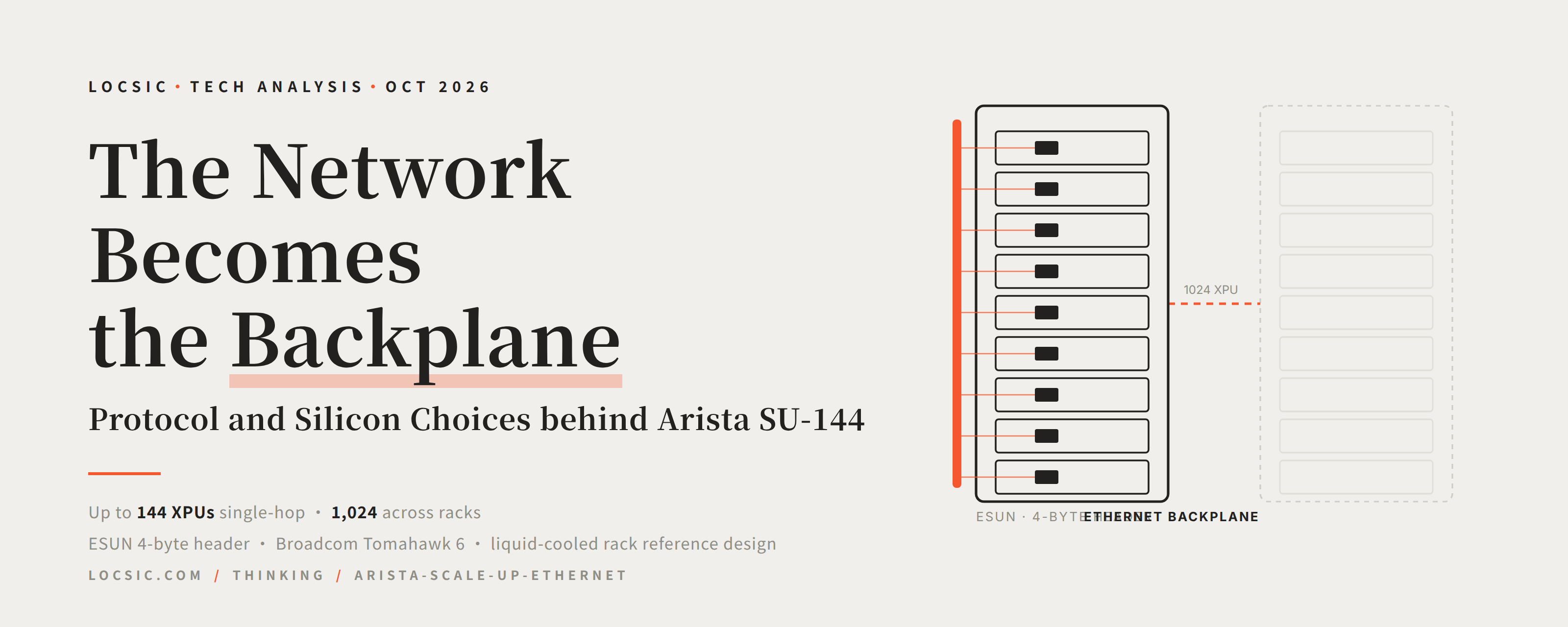
— Protocol and Silicon Choices for Scale-Up Networking
Abstract: On October 7, Arista announced the SU-144 scale-up architecture: a single-hop domain of up to 144 accelerators, extendable to 1,024 across racks, using Ethernet as the backplane — alongside a liquid-cooled rack reference design. Two choices define the release. On protocol, ESUN reshapes Ethernet with a 4-byte header and link-level reliability, competing with memory-semantic UALink and proprietary NVLink. On silicon, Arista builds no switch chips of its own; the 7060XE7 line runs Broadcom Tomahawk 6. Whether scale-up revenue materializes still depends on real deployments by the open camp.
On October 7, 2026 — five days before the OCP Global Summit — Arista announced two complementary pieces: the Etherlink SU-144 scale-up architecture, which defines rack-scale accelerator interconnect; and a liquid-cooled rack reference design that packages switches, software, cooling, fiber management, power, and leak detection into a solution integrators can assemble, test, and deliver as a complete rack. The launch lineup includes AMD, Arm, Broadcom, d-Matrix, Meta, Microsoft, and Qualcomm.
For Arista, this is the biggest identity shift since its founding in 2004. For two decades its business model fit in one sentence: run the best merchant silicon with the best network operating system, and sell the best switches. AI has pushed the boundary of that model inside the rack — once inter-accelerator communication becomes the bottleneck, the network is no longer a pipe between servers but the backplane shared by every accelerator in the rack. Arista SVP Tyson Lamoreaux put it plainly in the press release: “The network in the AI era is no longer just an independent pipe between servers. It’s now a tightly integrated rack-scale backplane that is essential to maximizing compute.”
The launch deserves a careful teardown because it stacks three choices: Ethernet on protocol (ESUN), Broadcom on silicon (Tomahawk 6), and the rack on delivery (reference architecture plus validation suite). This article unpacks the three layers in turn, then the competitive landscape and revenue reality, and closes with judgment.
1. Two Announcements in One Day: SU-144 and the Rack Reference Design
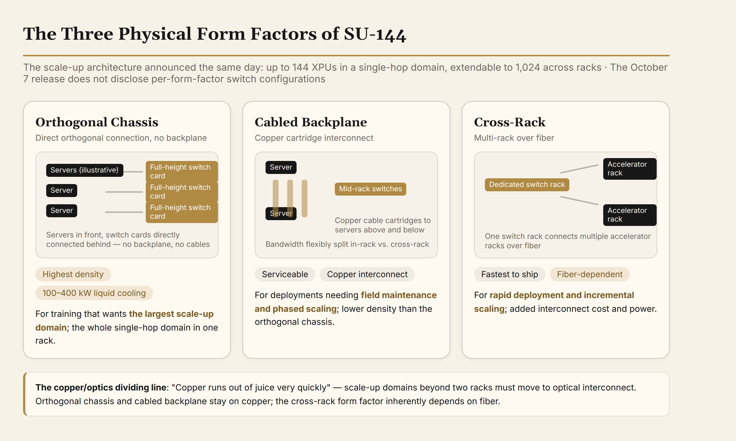
SU-144 is a scale-up architecture. It turns the accelerators of one rack — or several — into a shared compute domain: up to 144 XPUs (accelerators) in a single-hop network, extendable to 1,024 through cross-rack topologies. For comparison, NVIDIA’s current NVLink rack domains sit at the NVL72/NVL144 tier. Arista covers three classes of requirements with three physical form factors:
| Form factor | Structure | Characteristics | Best fit |
|---|---|---|---|
| Orthogonal chassis | Servers in front, full-height switch cards directly connected behind; no backplane, no cables | Highest density; 100–400 kW liquid cooling | Training that wants the largest scale-up domain |
| Cabled backplane | Switches mid-rack, connected via copper cable cartridges | Lower density but serviceable; bandwidth flexibly split in-rack vs. cross-rack | Field maintenance and phased scaling |
| Cross-rack | A dedicated switch rack connecting multiple accelerator racks | Fastest to ship; added interconnect cost and power | Rapid deployment, incremental scaling |
Notably, the October 7 release only describes the structure of the three form factors and does not disclose which switches each uses or how they are cabled. Arista’s switching foundation sits in the other half of the announcement.
The same day also brought a scale-out rack reference design. Here the hardware is explicit: 8, 12, or 16 liquid-cooled 7060XE7-series switches per rack (102.4 Tbps each), plus fiber patch panels, cooling manifolds, drip trays with active leak detection, a rack management controller, and power shelves with battery backup. The scale-out fabric supports Ultra Ethernet Consortium (UEC) standards, Multipath Reliable Connection (MRC), multi-plane routing, and dynamic/cluster load balancing — and explicitly supports coexistence of multiple scale-up protocols: ESUN, NVIDIA’s NVLink, NVLink Fusion, even PCIe. In other words, Arista is fine with the “NVLink domain plus Ethernet scale-out” combination.
Both halves share one delivery model. A 16-switch rack configuration involves roughly 2,000 fibers; on-site cabling invites bend-radius violations, misplugs, signal-integrity problems, and dead optics. Arista senior product line manager Arihant Jain’s verdict: “The whole old approach of spare parts or things assembled at site has to change.” Racks must be integrated and tested upstream, then shipped whole. Liquid cooling makes this a hard requirement: switches, cooling manifolds, and leak response must be designed together — when a leak is detected, do you shut down one switch or a row of racks? Should that decision be wired into the building management system? These used to be facilities questions; now they are network questions. By Arista’s analyst-briefing expectations, 100T-class switches will be roughly half liquid-cooled next year, and at the 200T tier liquid cooling effectively becomes mandatory.
Arista’s role therefore becomes: supply the switches, the software (its own EOS or an open NOS), and the design documentation; Netdi provides a unified diagnostics-and-telemetry foundation that delivers the same hardware-level diagnostics whether EOS or SONiC runs on top. By Arista’s account, Netdi represents more than 8,000 person-years, covering signal-integrity validation, secure-boot attestation, single-event-upset resilience, and optics-and-cooling monitoring. In a fully pre-integrated rack delivery, these hardware-level validation capabilities directly determine whether a rack lights up on arrival. Integrators deliver the complete rack.
The physical-layer roadmap came along too: today’s OSFP pluggable optics deliver about 1.6 Pb/s per rack; the next generation — XPO pluggables plus open CPO/NPO (co-packaged/near-packaged optics) — raises that to 6.5 Pb/s per rack, cutting data-center footprint nearly in half.
The product line’s timeline has three layers. Chip: Broadcom Tomahawk 6 sampled in mid-2025 and was declared in volume production in March 2026. Switch: the 7060XE7 series launched in June, with phased availability — the 64-port 1.6T air-cooled model in Q4 2026, the 64-port liquid-cooled and 128-port 800G models in Q1 2027. Rack: what shipped on October 7 is a reference architecture and validation suite, with full racks demonstrated at the OCP summit.
Copper is the physical dividing line. Vijay Vusirikala, who leads AI systems at Arista, put it in the analyst briefing as “copper runs out of juice very quickly” — scale-up domains beyond two racks must move to optics. This sets the long-run ordering of the three form factors: orthogonal chassis and cabled backplane are primarily copper; the cross-rack form factor inherently depends on fiber.
2. Where Protocol Choice Begins: What a Scale-Up Network Needs
The difference between scale-up and scale-out is not bandwidth but coupling. A scale-out network connects independent compute nodes carrying relatively loose distributed traffic; a scale-up network turns the accelerators of one or more racks into a shared compute domain carrying high-frequency, synchronized collectives (all-reduce, all-to-all). That defines the technical profile. Arista CEO Jayshree Ullal and chief development officer Hugh Holbrook summarized three traits in the blog that launched ESUN: highest bandwidth and lowest latency in the cluster; hop count pressed to a minimum (typically single-hop in-rack); reliable, in-order delivery.
These allow targeted simplification — but “simplification” does not mean deleting the reliability problem. Ethernet’s division of labor inside a scale-up domain has two layers. The network layer can shrink headers and simplify forwarding: bit-error drops are repaired at link level by LLR (link-level retry), and buffer overflow is prevented at the source by CBFC (credit-based flow control). But once the domain outgrows a single switch’s radix, or the per-accelerator lane budget runs short, hierarchical multi-hop topologies enter — ESUN 1.0 writes hierarchical topologies, transient and persistent congestion control, and path-level failure recovery into its requirements. The endpoint layer owns end-to-end reliability: the spec states plainly that drops beyond bit errors “will still need to be handled by end-to-end recovery mechanisms.” In other words, a smaller Ethernet header does not automatically produce a reliable shared-memory system; it provides a low-overhead, deterministic data path, while transactions, ordering, and retransmission at the endpoint are the XPU-side transport stack’s job.
History offered three answers. PCIe is the “local” interconnect, adequate between a CPU and in-server accelerators; Arista’s press release opens by citing “the limits of local PCIe and proprietary interconnects” as the motivation — a claim about rack-scale interconnect requirements. NVLink is the only proprietary scale-up fabric validated at scale; precisely because it succeeded, every other accelerator vendor needs an answer of its own.
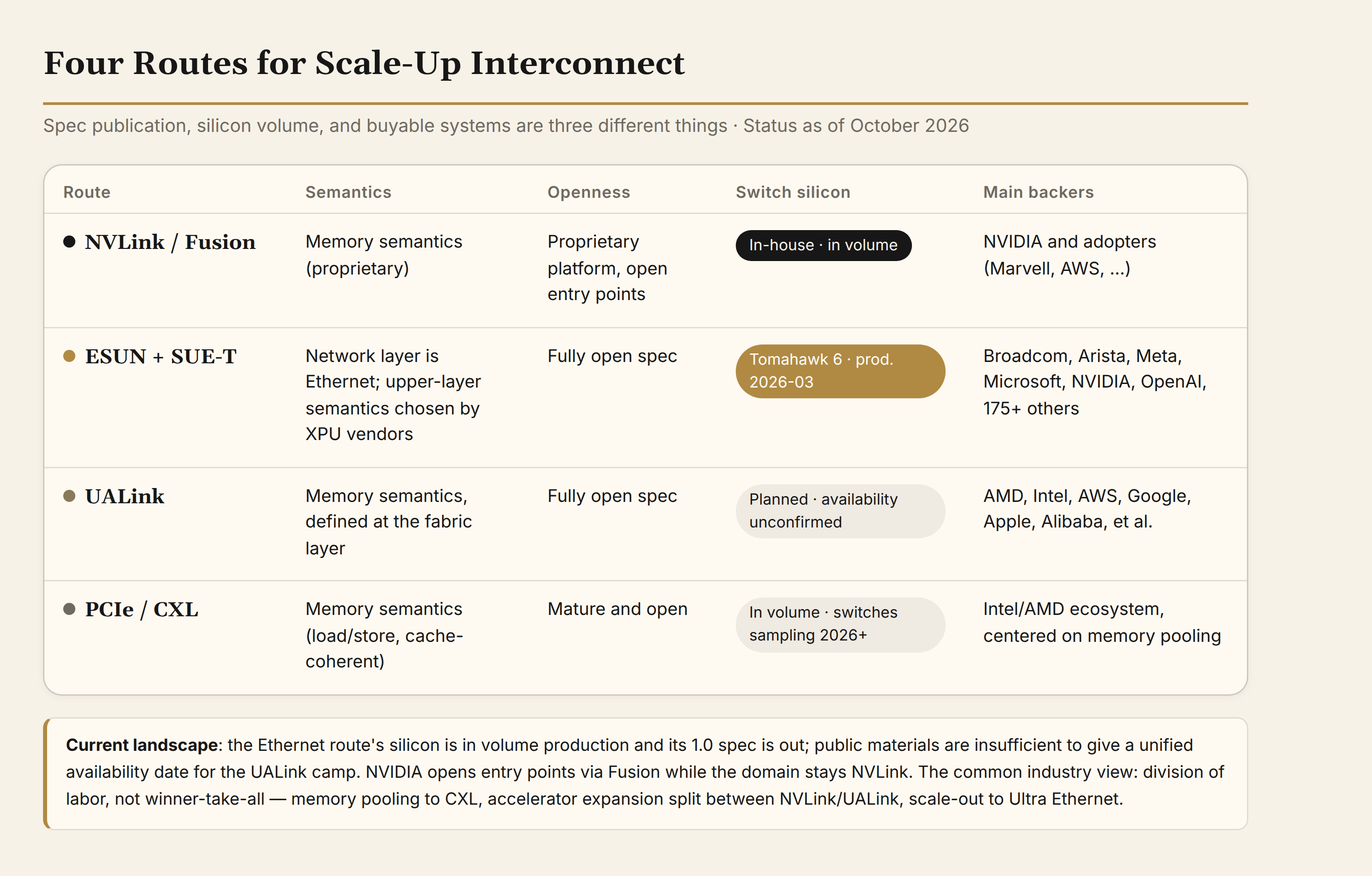
By October 2026 that answer converges on three active routes: NVLink Fusion (a proprietary platform with open entry points), UALink (open memory semantics), and ESUN plus SUE-T (open Ethernet). PCIe/CXL keeps its center of gravity in-chassis and in memory pooling.
3. Four Routes and Their Trade-offs
Maturity must be read in layers — spec publication, silicon volume, and buyable systems are three different things, and merging them into one column misleads:
| Route | Spec status | Switch silicon | Main backers |
|---|---|---|---|
| NVLink / NVLink Fusion | Proprietary platform, open entry points | In-house, in volume production | NVIDIA and adopters |
| ESUN + SUE-T | ESUN 1.0 (finalized 2026-02); SUE-T evolving | Tomahawk 6 in production (announced 2026-03) | Broadcom, Arista, Meta, Microsoft, NVIDIA, OpenAI, and 175+ others |
| UALink | 1.0 (2025-04); 2.0 (2026-04) | Materials gathered here are insufficient to confirm volume availability; spec progress and vendor delivery must be checked separately | AMD, Intel, AWS, Google, Apple, Alibaba, et al. |
| PCIe / CXL | Mature and open | In production (PCIe 6.0/CXL switches sampling from 2026) | Intel/AMD ecosystem, centered on memory pooling |
NVLink Fusion: widening vertical integration through “horizontal openness.” Fusion launched at Computex in May 2025 around an interconnect chiplet with up to 1.8 TB/s bidirectional bandwidth. The logic is straightforward: vendors building their own XPUs or CPUs can join an NVLink domain — XPUs attach via the UCIe standard interface to an NVIDIA bridge chiplet, CPUs via NVLink-C2C. What you join is the interconnect-and-rack layer of the platform; NVIDIA’s technical documentation is equally clear that Fusion ships as a modular OCP MGX rack solution that “enables NVLink Fusion integration with any NIC, DPU, or scale-out switch.” The pace of adoption has been fast: the initial partners include Fujitsu, Qualcomm, MediaTek, Alchip, Astera Labs, Synopsys, and Cadence; Samsung Foundry joined in October 2025, Arm in November (licensees can now build CPUs that ship with NVLink ports), and RISC-V player SiFive in January 2026. On March 31, 2026, NVIDIA announced a $2 billion investment in Marvell and a strategic partnership: Marvell provides custom XPUs and NVLink Fusion-compatible scale-up networking, NVIDIA provides the supporting technologies including the Vera CPU, ConnectX NICs, BlueField DPUs, NVLink interconnect, and Spectrum-X switches — note this is the division of labor for that one partnership, not a mandatory bill of materials for every Fusion user. The more consequential datapoint is AWS: NVIDIA’s December 2025 blog update disclosed that AWS is adopting NVLink Fusion to build the semi-custom rack infrastructure for Trainium4, while continuing to use its own Graviton CPUs, EFA NICs, and the Nitro hypervisor. It is an adoption announcement, not production acceptance — but the direction is clear.
For Arista the implication is direct: a non-NVIDIA accelerator does not automatically mean the open-Ethernet camp. Fusion is pulling the most capable delivery organizations into NVIDIA’s rack-and-interconnect orbit — even where scale-out NICs and switches remain free choices, the scale-up domain’s interconnect is now built on NVLink.
ESUN plus SUE-T: re-engineering Ethernet into a scale-up foundation. ESUN (Ethernet for Scale-Up Networking) is an OCP workstream launched in October 2025 by twelve companies: AMD, Arista, Arm, Broadcom, Cisco, HPE, Marvell, Meta, Microsoft, NVIDIA, OpenAI, and Oracle. Note NVIDIA’s presence — it sells NVLink on one side while keeping a seat in the Ethernet standards body, a textbook hedge. ESUN 1.0 was finalized in February 2026 and released in March; participation has grown past 175 companies, with Meta and Microsoft leading the initial specification.
ESUN’s structure has three layers: a common Ethernet header (for interoperability), an open Ethernet data-link layer (LLR, PFC, CBFC — the lossless reliability mechanisms directly reference the UEC 1.0 spec), and the commodity Ethernet PHY. The key new element in 1.0 is the ESUN Header: a compact 4-byte header that, per the OCP announcement, replaces the IP/UDP header stack of typically 28–48 bytes. Scale-up traffic carries many small synchronization messages, and header overhead eats bandwidth directly; the 4 bytes restore congestion feedback, class of service, flow label, and TTL.
ESUN’s most important design decision is restraint: it standardizes only “how Ethernet runs fast and lossless inside a scale-up domain” — encapsulation, error recovery, losslessness — and leaves upper-layer semantics to the XPU vendors: push or pull, memory or streaming semantics, whether the endpoint implements a full reliable transport (the SUE framework splits into a full version and a Lite version that keeps only per-hop LLR), ordering rules, congestion policy.
The endpoint layer is filled by SUE-T. Broadcom donated its SUE (Scale-Up Ethernet) framework to OCP in April 2025 (v1.0 followed in September); the framework was later split by layer: the fabric layer merged into ESUN, and the transport layer became SUE-T, responsible for reliable delivery and transaction packaging at the XPU endpoint; load balancing across SUE instances (across planes) is done by the XPU above the transport layer. The SUE framework’s endpoint instances carry one-sided memory transactions (put/get/atomic); each XPU can host multiple instances of 1–4 Ethernet ports each. Controlled topologies and pre-known endpoints allow static connections, one path per plane, and simple go-back-N retransmission, shrinking transport state dramatically. The document’s worked example — 64 XPUs, twelve 800G instances each, twelve switches — yields up to 9.6 Tb/s between any pair; the sub-2µs round-trip figure is a design target, not a measured result, and neither should be read as a property of any SU-144 system. SUE provides a unified network and command channel, but command sets are XPU-defined — two accelerators on the same SUE network do not thereby understand each other’s commands or share memory; endpoint semantics, software interfaces, and cross-vendor interop still require explicit agreement and validation.
UALink: memory semantics in an open spec, stuck on the calendar. The difference from ESUN is fundamental: ESUN specifies how the network runs and leaves endpoint semantics to XPU vendors; UALink defines memory semantics at the fabric-spec layer — load/store/atomic operations, 64–256-byte transaction granularity, a 57-bit address space (128 PB directly addressable), software-managed coherence. Per the consortium white paper: 200G per lane, up to 1,024 endpoints, sub-microsecond round trips (about 1µs at 4m over copper), targeting 90%+ link utilization. For cross-accelerator memory pooling, fabric-native load/store has real value — the white paper sells exactly this against the Ethernet route.
UALink 1.0 shipped in April 2025; 2.0 in April 2026, split into four specs (Common 2.0 introducing in-network compute, 200G DL/PL for independent evolution, Chiplet, Management); 3.0 is planned for 2027 with higher bandwidth, cross-rack reach, and reliability. These dates reflect spec progress; adopters must separately confirm switch silicon, endpoint implementations, and system delivery. The public materials gathered here are insufficient to give one unified availability date for the UALink camp. The twelve board seats show who needs it: AMD, Astera Labs, AWS, Cisco, Google, HPE, Intel, Meta, Microsoft, plus Alibaba, Apple, and Synopsys (all joined January 2025) — mostly giants that “want their own accelerators without being locked to any single platform,” together with the connectivity, systems, and IP vendors that support the ecosystem.
PCIe and CXL: center of gravity in-chassis and in memory pooling. CXL 4.0 (November 2025) doubles bandwidth to 128 GT/s and introduces port bundling, aiming at cross-rack memory composition; Marvell launched a CXL switch and a 260-lane PCIe 6.0 switch at OFC 2026 (sampling Q3 2026). But this route’s current position is not the XPU backbone: per Astera Labs’ August 2026 earnings call, CXL memory controllers reach volume shipment and meaningful revenue in 2027, with memory pooling and AI-inference KV-cache exploration before that. Worth noting on the demo side: Astera showed a PCIe 6 switch with linear pluggable optics (LPO) across racks at Computex 2026 — link-level feasibility is demonstrated; domain-scale deployment and acceptance evidence is not yet public.
Ethernet’s present advantage is a reusable supply chain. PHY, SerDes, optics, switch silicon, and operations tooling all have mature suppliers; ESUN does not need to rebuild a physical-layer industry. UALink need not start from the physical layer either — Credo’s 224G multiprotocol retimer supports both UALink and ESUN, showing the two open routes can share physical-layer components. Their main difference lies above the link: protocol, endpoint implementation, and interop validation.
Tomahawk 6 is in production and ESUN 1.0 is out, letting vendors build products around existing silicon. Others are entering: Upscale’s Token Fabric, announced October 8, includes the SkyFabriX switch chip with announced support for ESUN, SUE-T, and UALoE, with the whole platform planned for early-2027 availability; UALink is listed as an evolving support item, and the announcement gives no delivery date for it. The case shows Ethernet scale-up suppliers multiplying; it cannot be used to date the UALink industry’s availability.
For high-frequency collectives, SUE’s controlled topology, static connections, and lean transport have clear engineering appeal. Whether adoption pays off depends on how much effective bandwidth, tail latency, and failure recovery the designs deliver on target training or inference workloads. Existing silicon and specs shorten the distance from starting point to product; endpoint and system validation still gate the last mile.
But this is not the endgame. Memory semantics is not a manufactured need: cross-accelerator memory pooling, KV-cache sharing, and parameter-plane synchronization are all scenarios where fabric-native load/store pays off. UALink 3.0 pushes higher bandwidth and cross-rack reach in 2027, CXL 4.0 holds memory pooling, and NVLink Fusion absorbs custom XPUs. The industry consensus is fragmentation through at least 2027: memory pooling to CXL, accelerator expansion to NVLink/UALink, scale-out to Ultra Ethernet — no single standard takes everything.
4. Silicon Choice: Twenty Years Without an In-House Chip, Now the Rack Line Rides Broadcom
Arista is the most thorough practitioner of the merchant-silicon model: it designs no forwarding silicon of its own and bets its differentiation on EOS software. Andy Bechtolsheim’s (2009) silicon-choice blog says it verbatim: “we have achieved all of this without spending a dollar on custom chip development.” The method is to write the next-generation NOS first, then pick the best merchant silicon available — which, per Arista, kept its products ahead on cost-performance versus proprietary-ASIC rivals. The product line splits cleanly: the 7060 series uses Broadcom Tomahawk (low latency, high bandwidth); the 7280R/7800R series uses Broadcom Jericho (deep buffers, cloud routing).
In the new scale-up arena, that tradition resolves into one concrete choice. When Arista launched the 7060XE7 series in June, Broadcom core-switching GM Asad Khamisy’s quote was unambiguous: Broadcom powers Arista’s 1.6T Ethernet solutions with the Tomahawk 6 102.4T switch, “enabling optimized scale-up and scale-out connectivity.” Arista’s own framing: unlock Tomahawk 6’s on-chip resources and features while preserving software consistency across EOS or open NOS, turning the switches into “a unified rack-scale radix.” In other words, the switching foundation of Arista’s rack line is the 7060XE7 (Tomahawk 6), a family aimed at both scale-up and scale-out. The October release does not disclose per-form-factor switch configurations for SU-144 — that becomes clear only in customer co-design and production.
Tomahawk 6 itself is the first 102.4T switch chip announced in volume production (Broadcom’s claim):
- 512 200G SerDes (or 1,024 100G);
- a single chip can single-hop all-to-all connect 512 XPUs (200G per link, running SUE) — an illustrative radix figure;
- two-tier scale-out networks cover 128K XPUs;
- native unified scale-up/scale-out: the same ports can be repartitioned between the two uses (Broadcom’s “fungible interfaces” — operators can carve XPU estates into domains of the right size);
- Cognitive Routing 2.0 load balancing and congestion management, plus a CPO variant (Davisson).
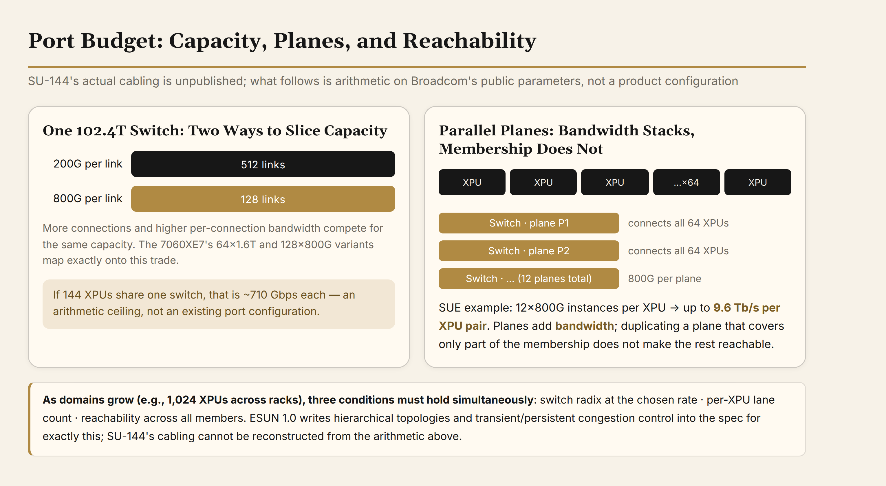
It pays to compute how switching capacity, port rate, and domain size constrain each other. A single 102.4 Tb/s switch has fixed capacity: at 200 Gb/s per link it corresponds to 512 links; at 800 Gb/s, 128. More connections and higher per-connection bandwidth compete for the same capacity. If 144 XPUs share one switch, the ~710 Gb/s per XPU is only an arithmetic ceiling; real configurations must still satisfy port rate and port count. Parallel planes raise per-XPU aggregate bandwidth: in SUE’s 64-XPU example, each plane’s switch connects all 64 XPUs, and twelve 800G planes stack to 9.6 Tb/s per pair. Planes add bandwidth, not members — duplicating a plane that covers only part of the membership does not make the rest reachable. As domains grow, switch radix at the chosen rate, XPU lane count, and reachability across all members must all be satisfied; ESUN permits hierarchical topologies when needed, and SU-144’s 1,024-XPU cabling is unpublished — none of this arithmetic reconstructs it. The 7060XE7’s 64×1.6T and 128×800G variants illustrate the port-count-versus-port-rate trade directly.
Why the choice is right. First, timing: designing a chip in this class takes years, and the market window is one or two; TH6 sampled mid-2025, hit volume production in March 2026, Arista’s switches phase in within the year, and the rack architecture follows. Second, ecosystem: Broadcom supplies the chip and co-authored the spec; Arista reuses existing silicon features and protocol implementation resources rather than building from zero — XPU-side protocol implementation and cross-vendor integration still require combined validation. Third, competition: Accton and other ODMs use the same TH6, Cisco has Silicon One, NVIDIA has Spectrum — rack-scale competition is not about port speed (everyone lands in the 102.4T class); it is about software, operations, and delivery. Hardware homogeneity moves the battlefield to where Arista is strongest.
The costs are equally clear. First, the binding deepens. Everything Arista stakes on Ethernet — EOS, rack engineering, validation suites — is built on Broadcom’s silicon. And Broadcom is the biggest multi-bettor in the race: it donated SUE-T (the Ethernet route); it is also building the 10 GW-class custom XPU program with OpenAI (announced October 2025, deploying through 2029). Whichever route wins, Broadcom’s IP, PHY, and custom-silicon business has plenty to sell; Arista’s stake sits on the Ethernet route alone. Second, if the scale-up backbone ends up UALink (memory semantics, non-Ethernet MAC), Arista’s Ethernet software-stack advantage dilutes, and it must wait for vendors to ship UALink switches before following. That is why Arista’s interests are genuinely tied to ESUN’s success — it is one of the twelve founders, and the CEO blogs the case personally. A further datapoint: Upscale, reportedly backed by NVIDIA (per The Next Web), lists ESUN/SUE-T as its first-generation SkyFabriX chip’s launch protocols — multi-betting is the norm in this industry, and Arista is no exception.
The hedge is not to build a chip but to deepen “protocol-agnostic delivery capability”: Netdi’s diagnostics apply equally to open NOS, and the scale-out side explicitly supports NVLink, NVLink Fusion, and PCIe domains. Rack engineering, liquid cooling, fiber management, validation, and operations are work every scale-up deployment must complete; Arista’s strategy is to have that work flow to itself, whatever protocol the customer’s scale-up domain chooses.
The real moat sits at that layer. SiliconANGLE’s analysis hits the key point: scale-up, scale-out, and scale-across run on the same EOS, telemetry, and diagnostics, extending fault isolation and predictive maintenance into the most sensitive part of the cluster — while Fusion opens only the entry point; inside the scale-up domain it is still NVLink. That operational openness is Arista’s strongest pitch to customers.
5. Competition and Revenue: Scale-Up Is an Option, Not Cash Flow
NVIDIA’s counterattack is accelerating. The Fusion roll call — Qualcomm, MediaTek, Marvell, Arm, SiFive, Samsung Foundry, plus AWS’s Trainium4 in adoption — shows the point. Arista’s opportunity therefore depends on the size of the “independently minded” slice of the heterogeneous camp: hyperscaler in-house accelerators like Microsoft Maia and Meta MTIA, plus neoclouds. Vusirikala’s read on the NVIDIA ecosystem is equally blunt: “There is no near-term opportunity because that is proprietary.”
Revenue deserves a clear-eyed read. Arista’s Q2 2026 (reported early August):
- Quarterly revenue of $3.036 billion, up 37.7% year over year — the first $3B quarter, beating guidance;
- Full-year guidance raised for the third time this year, to about $12.6 billion (+40%);
- The 2026 AI Fabric revenue target is at least $3.5 billion, with 100+ cumulative Etherlink customers;
- The fastest-growing new business is scale-across (cross-datacenter networking), about 30% of the 2026 AI target.
Putting these numbers next to SU-144, the split matters: Arista’s AI Fabric revenue currently comes from scale-out and scale-across; the company as a whole also runs campus and other businesses (2026 target: at least $1.25 billion). Meaningful scale-up rack revenue, on current disclosure pace, is likelier after 2027 — this article’s judgment, not management guidance. What SU-144 delivers today is positioning: getting the reference architecture, validation suite, and operational consistency onto customers’ evaluation shortlists before the heterogeneous camp picks a network foundation.
Two near-term windows: the OCP Global Summit, October 12–15 (Arista’s booth shows the full liquid-cooled rack; co-founder Andy Bechtolsheim gives a breakout session, “The Gigawatt AI Data Center Era,” on October 13), and the Q3 report in early November.
6. Judgment
One: this is the most consequential identity expansion in Arista’s history, decided by deployments rather than launches. Between “sell the best switch” and “define the network platform inside the AI rack” lies a real gulf: open designs require accelerator vendors, rack integrators, and cooling suppliers to coordinate, while NVIDIA sells turnkey systems — Ethernet does not always make it into the procurement discussion. The observation point is 2027: whether large clusters built from multiple 144/1,024-XPU domains land in the AMD, Microsoft Maia, or Qualcomm camp. The OCP Summit demos on October 12–15 and the quality of AI orders in the November Q3 report are the first leading indicators.
Two: the physics applies to every route; Ethernet’s edge is speed of execution. As domains grow and per-link rates climb, high-speed links quickly exceed passive copper’s reach (Vusirikala’s call), making optics increasingly necessary; power density pushes liquid cooling toward mandatory (per Arista’s expectations, ~50% of 100T-class switches liquid-cooled next year, effectively required at 200T). These constraints favor no protocol — everyone needs optics, liquid cooling, and pre-integrated racks. The difference is the path to delivery: Ethernet’s supply chain for PHY, optics, switch silicon, and tooling exists and competes, shortening the distance from engineering need to product. That is an opportunity, not a guarantee. The software layer needs no early verdict either: UALink 3.0 pushes bandwidth and cross-rack reach in 2027, CXL 4.0 holds memory pooling, and NVLink Fusion absorbs custom XPUs. The likeliest shape of the next two or three years is division of labor, not winner-take-all: scale-out to Ethernet, scale-up split among three routes by workload, memory pooling to CXL. For deployers, the more useful conclusion is the one Arista itself concedes — protocols can coexist; operational consistency is the real stickiness it sells.
Three: for China’s domestic compute ecosystem, this is a directly reusable template — but not the only road. ESUN and SUE-T are fully open spec stacks. When domestic accelerator vendors need scale-up networking, every layer of this road — specs, switch silicon, PHY, optics, operations models — has incumbent suppliers and multi-vendor competition, saving the effort of defining an interconnect from scratch and nurturing a chip ecosystem; the integrator still owns endpoint semantics, integration validation, and operational consolidation, which cannot be skipped. The parallel road deserves equal attention: Huawei has announced it will open-source its unified interconnect protocol UB-Mesh (Unified Bus, paired with the SuperPoD architecture, technical papers public), targeting replacement of PCIe, CXL, NVLink, and TCP/IP, with its main arena in the Chinese market. The Chinese camp is both a potential user of open standards and an exporter of its own. The two roads do not conflict — which one works will be decided by real-cluster workloads.
Sources and computation notes: This article draws on public materials available before October 9, 2026; no hardware testing was performed. Chinese quotes are translations; verbatim originals are at the cited sources.
- Arista press release, 2026-10-07 (SU-144’s 144/1,024 XPU, three form factors, the scale-out rack’s 7060XE7/102.4T and MRC/DLB/CLB, XPO and open CPO/NPO at 1.6→6.5 Pb/s, multi-protocol coexistence): https://www.arista.com/en/company/news/press-release/24818-pr-20261007
- Arista technical blog same day (Jain/Vusirikala: the five rack-scale fabric requirements, Netdi’s diagnostics role and 8,000 person-years, beyond 72/144 XPUs): https://blogs.arista.com/blog/next-gen-scale-up-networking-for-ai-fabrics
- Arista press release, 2026-06-09 (7060XE7=TH6, Khamisy and Lamoreaux quotes, Azure Maia/Fairwater, Meta, Oracle endorsements, LPO saving ~60% interconnect power): https://www.arista.com/en/company/news/press-release/24102-pr-20260609 ; model phasing (64PS/64PRS Q4’26, 64PRS-RV3-L/128PE Q1’27) per the product page https://www.arista.com/en/products/7060xe7-series and thedatacenterengineer.com
- SiliconANGLE analysis same day (form-factor engineering detail, Vusirikala/Jain quotes, ~2,000 fibers, the 50/50 liquid-cooling split and 200T mandate, the operational-consistency argument, the procurement caveat): https://siliconangle.com/2026/10/07/arista-takes-ethernet-rack-network-becomes-backplane
- OCP ESUN 1.0 announcement (EH replacing the typically 28–48-byte IP/UDP header stack, PFC/CBFC/LLR, 175+ companies, twelve founders, Meta+Microsoft leadership): https://www.opencompute.org/news/the-ocp-esun-10-specification-has-been-released/ ; ESUN 1.0 spec PDF (hierarchical-topology and transient/persistent congestion requirements, drops beyond bit errors needing end-to-end recovery, EH-ECN/CoS/Flow Label/TTL, MACsec): https://www.opencompute.org/documents/ocp-esun-network-operator-requirements-base-specification-rev-1-0-final-pdf
- Arista blog “The Sun Rises on Scale-Up Ethernet” (2025-10-13, Ullal/Holbrook: the three-layer structure, three traits, SUE-T’s positioning): https://blogs.arista.com/blog/the-sun-rises-on-scale-up-ethernet
- Broadcom SUE framework RM104 (the 64-XPU×12×800G example and 9.6 Tb/s, the <2µs design target, one-sided memory transactions, static connections and go-back-N, SUE Lite, XPU-specific command sets with no cross-XPU interop defined): https://docs.broadcom.com/doc/scale-up-ethernet-framework ; Broadcom’s technical article on the SUE→SUE-T split: https://www.broadcom.com/topics/what-are-the-ethernet-standards-for-ai-infrastructure
- Broadcom Tomahawk 6 volume-production release (2026-03-12, under three quarters from initial sampling to production, 512-XPU single-hop, 128K two-tier, 512×200G SerDes, Cognitive Routing 2.0, CPO option): https://investors.broadcom.com/news-releases/news-release-details/broadcom-now-shipping-worlds-first-1024-tbps-switch-production
- UALink white paper (64–256-byte transactions, 57-bit addressing, ~1µs at 4m copper, 90%+ utilization, the contrast with the Ethernet route): https://ualinkconsortium.org/wp-content/uploads/2026/01/UALink_White_Paper_Publication_FINAL_UPDATED.pdf ; UALink 2.0 release (2026-04-07, four specs, In-Network Compute in Common 2.0): https://ualinkconsortium.org/wp-content/uploads/2026/04/UALink-2.0-Specification-PR_FINAL.pdf ; board roster: https://ualinkconsortium.org/specification
- NVIDIA×Marvell partnership release (2026-03-31, $2B investment, the partnership’s division of components, silicon photonics and AI-RAN): https://nvidianews.nvidia.com/news/nvidia-ai-ecosystem-expands-as-marvell-joins-forces-through-nvlink-fusion ; NVIDIA Fusion technical blog (any NIC/DPU/scale-out switch, UCIe attach, AWS Trainium4 “is adopting,” the 72-GPU domain at 1,800 GB/s): https://developer.nvidia.com/blog/scaling-ai-inference-performance-and-flexibility-with-nvidia-nvlink-and-nvlink-fusion/ ; the adoption timeline and commentary: https://thenextweb.com/news/nvidia-marvell-nvlink-fusion-ecosystem-lock-in
- Upscale Token Fabric announcement (2026-10-08, SkyFabriX supporting ESUN/SUE-T/UALoE, UALink “evolving,” GA early 2027, d-Matrix endorsement; the date is not a UALink delivery date; NVIDIA’s investment per The Next Web and Reuters): https://upscale.com/blogs/upscale-introduces-token-fabric-the-industrys-most-comprehensive-standards-based-networking-portfolio-for-ai-factories , HPCwire cross-check https://www.hpcwire.com/off-the-wire/upscale-unveils-token-fabric-to-unify-scale-up-and-scale-out-ai-networking , NVIDIA investment reporting https://thenextweb.com/news/upscale-ai-token-fabric-nvidia-ai-chip-networking
- Astera Labs Q2 2026 earnings-call view (CXL volume revenue 2027) and the Computex 2026 PCIe 6+LPO cross-rack demo: https://www.asteralabs.com/resources/blog/computex-2026-demo-how-linear-optics-enables-longer-link-reach-lower-latency-for-scorpio-smart-fabric-switches/ ; Marvell OFC 2026 (CXL/PCIe 6.0 switches, Q3’26 sampling) via Yahoo Finance
- CXL 4.0 (2025-11-18) and the fragmentation view: https://introl.com/blog/cxl-4-specification-interconnect-wars-ai-memory-december-2025 ; Credo 224G multiprotocol retimer (2026-01, UALink/ESUN/Ethernet): https://ualinkconsortium.org/news (member news)
- Arista blog “The Silicon Choice for Cloud Networking” (“not a dollar on custom chips”): https://blogs.arista.com/blog/the-silicon-choice-for-cloud-networking ; Broadcom-OpenAI 10GW: CNBC, 2025-10-13
- Arista Q2 2026 results and call ($3.036B/+37.7%, $12.6B guide, AI ≥$3.5B, campus ≥$1.25B, scale-across ~30%, 100+ customers): https://investors.arista.com/Communications/Press-Releases-and-Events/Press-Release-Detail/2026/Arista-Networks-Inc--Reports-Second-Quarter-2026-Financial-Results/default.aspx and alpha-sense/Motley Fool transcripts
- Huawei UB-Mesh: https://www.tomshardware.com/tech-industry/artificial-intelligence/huawei-to-open-source-its-ub-mesh-data-center-scale-interconnect-soon-details-technical-aspects-one-interconnect-to-rule-them-all-is-designed-to-replace-everything-from-pcie-to-tcp-ip ; paper https://arxiv.org/html/2503.20377v1
- This article’s judgments (the two-layer reliability split, the three reasons for Ethernet’s current edge and their verification conditions, the port-budget ceiling framing, the binding-and-hedge analysis, the scale-up revenue-option reading, the domestic-ecosystem and UB-Mesh parallel) are the author’s synthesis. The capacity arithmetic (102.4T÷144≈710G) is derivation, not disclosed configuration; SU-144’s 1,024-XPU cross-rack topology is unpublished, and the generic port budget here is not a product architecture.